
CHAPTER 13
Immobilization of Biomolecules at Semiconductor Interfaces
13.1 INTRODUCTION
Many emerging applications in biotechnology and biological/environmental sensing require surfaces that are highly selective and stable. The integration of biomolecules such as DNA and antibodies onto semiconductor surfaces provides several potential benefits. For example, semiconductors such as silicon are extremely pure and homogeneous, and can be used as highly reproducible substrates. Semiconductors such as silicon can be conveniently processed, etched, and manipulated using the tools developed for microchip fabrication, and translated toward biochips. In principle, it should be possible to take advantage of the unique properties that semiconducting materials can offer. Of these, one of the most important is the ability to amplify small changes in voltage or charge density and thereby convert biological information into measurable electrical signals in a highly parallel and low-cost manner. As one example, an inexpensive electronic voltmeter can read potential to four significant digits and costs less than $10. A current-generation microprocessor has over 2 billion transistors, each of which is a sensitive amplifier of current or voltage. If biological systems could be truly integrated with semiconductor-based materials, it could provide new opportunities for highly parallel biological detection. In the near term, bioelectronic devices are of interest for applications such as realtime monitoring of pathogens [1].
Self-assembled monolayers on gold have been widely studied because goldthiol chemistry provides a convenient pathway toward well-ordered molecular layers [2–4]. Yet, many emerging applications require semiconducting substrates because of their unique electronic, optical, or mechanical properties. The integration of organic and biological molecules with covalent materials such as silicon and diamond presents new opportunities for making ultrastable highly selective surfaces. While silicon is the foundation of the microelectronics industry, diamond is an extraordinarily stable material even in water and is also a transparent, wide bandgap semiconductor. In each case, the challenge is to start with highly stable materials and make them “smart” by developing and implementing new surface modification strategies.
Here we will review recent and ongoing research on the formation of biomolecular interfaces to semiconducting materials.
13.2 MOLECULAR AND BIOMOLECULAR INTERFACES TO SEMICONDUCTORS
Silicon has long been a substrate of high interest because of the possibility of combining the extensive infrastructure of microelectronics for patterning and device fabrication with the study of biological systems [5–8]. The ability to convert biological information directly into electrical signals without the need for fluorescence or optical detection schemes is extremely attractive and remains a driving force behind much of the research in biological surface chemistry of semiconductors.
Of all the semiconductors, silicon is by far the most heavily studied because of its widespread use as the foundation for the vast majority of today's microelectronic devices such as microprocessors and memory chips. In addition, silicon has attracted attention as a substrate because the availability of relatively low-cost crystalline material with extremely high purity can provide a reliable starting point. Furthermore, etching and deposition procedures provide the ability to construct MEMS (microelectromechanical system) structures such as flow channels [9]. The ability to grow single-crystalline silicon nanowires has also led to a number of nanowire-based biosensing systems [10].
One of the biggest challenges associated with interfacing biological systems with semiconductor materials arises because while microelectronic device processing is typically done under dry environments and in tightly controlled atmospheric conditions, biological studies are performed under aqueous (and typically salty) environments. This presents two problems. First, controlling the surface chemistry to yield organic-to-semiconductor interfaces that will be stable under these conditions. Second, the electrical properties of semiconductors are often quite sensitive to the presence of electronic states lying within the bandgap, such that successful implementation of direct biological-to-electrical signal transduction requires careful attention to both the chemical and the electrical properties at the interface [11,12].
13.2.1 Functionalization Strategies
In general, one of the biggest challenges in making biological interfaces to semiconductors is that most semiconductor materials are not thermodynamically stable in the presence of water. For example, silicon reacts with water to form SiO2, which in turn slowly hydrolyzes in H2O to form silicic acid (Si(OH)4) and other water-soluble silicon species [13–17]. Similarly, the interfacial bonds used in linking (bio)molecular systems to bulk semiconductors, such as Si–O–C [18] or Ti–O–C linkages, are often subject to slow hydrolysis in aqueous environments. Consequently, the design of stable biomolecular architectures requires careful attention to the stability of the interface.
There are four main approaches that are used to produce molecular layers for biological applications of semiconductors:
- Use of the most stable materials and chemical bonds possible (e.g., diamond).
- Multidentate bonding to the surface (e.g., phosphonate and/or siloxane layers).
- Lateral cross-linking between surface-bound molecules to form a two-dimensional surface net [19].
- Use of molecules bearing hydrophobic regions that act as barrier layers to keep reactive species away from the interface [19].
These four approaches are used to varying extents in all successful surface functionalization strategies. Almost all successful methods have some degree of lateral cross-linking and use hydrophobic barrier layers. Yet these different strategies differ greatly in the level of control, reproducibility, versatility, and stability that they provide. Figure 13.1 summarizes the most commonly used approaches to functionalizing semiconductor surfaces. They include the use of organosilane compounds (Fig. 13.1a), phosphonic acid derivatives (Fig. 13.1b), grafting of terminal alkenes to hydrogen-terminated surfaces (Fig. 13.1c), grafting of terminal alkenes to hydroxy-lated surfaces of metal oxides (Fig. 13.1d), and use of aryldiazonium salts (Fig. 13.1e).
13.2.2 Silane Derivatives
Since silicon oxidizes readily and is widely used as the gate material in microelectronic devices, one approach to making biomolecular interfaces on silicon has been to intentionally form a surface oxide layer and to construct biomolecular interfaces to the oxide. This is the simplest approach and has been the most widely used. The oxide that forms spontaneously upon contact with air and/or water, typically referred to as the “native” oxide, has a thickness on the order of 1 nm [20,21] but has poor electrical quality due to the presence of large number of unsaturated “dangling bonds” at the interface and in the oxide. Hence, more often studies of this type have formed thicker, more stoichiometric SiO2 layers using thermal processing to oxidize the silicon [22]. While very early studies of silicon-based biosensors used non-functionalized SiO2 (measuring instead changes in ion activity or pH) [5], in order to produce selective interfaces it is necessary to link more complex molecules such as DNA or proteins directly to the surface to provide surface-linked biomolecular recognition elements.
One common approach to forming biomolecular interfaces has been the use of silane derivatives, typically alkoxysilanes or alkylchlorosilanes, two of which are depicted in Fig. 13.1a [23–32]. These molecules react with hydroxyl groups on surfaces to form Si–O–X linkages, where X corresponds to the substrate material. Oxidized silicon surfaces expose substantial number of silanol groups (Si–OH) that are reactive toward the silanes [26]. The silane layers are typically deposited from solutions in methanol or other polar solvent. The deposition reactions are complicated by the fact that small amounts of water are necessary for the reaction to occur; some water is always present on the starting surfaces as a physisorbed layer, but water is also present (often unintentionally) in the solvent [33]. Thus, hydrolysis occurs in the bulk and also at the surface. Hydrolysis in the bulk produces polymeric materials that deposit on the surface in an inhomogeneous manner, forming clumps of deposited materials [34]. Reaction with the surface –OH bonds produces surface-bound monolayers with the extent of cross-linking versus surface binding varying depending on the number of hydroxyl groups on the surface and on the precise nature of the alkoxysilane chosen.
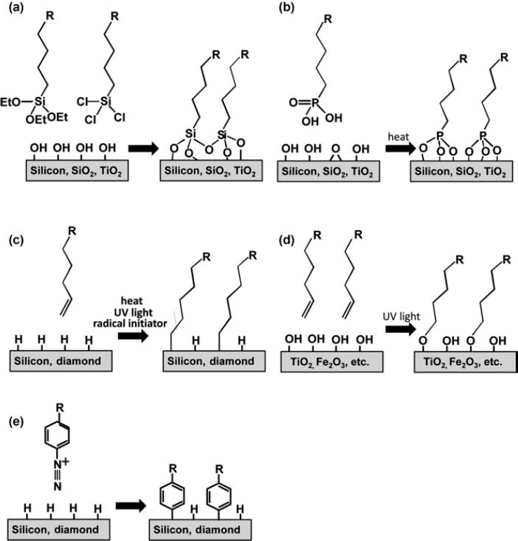
FIGURE 13.1 Schematic illustration of different schemes for making organic interfaces to semiconductors for biological application. (a) Use of alkoxysilanes and chlorosilanes, (b) phosphonic acid derivatives, (c) alkene grafting to H-terminated surfaces, (d) alkene grafting to hydroxide-covered surfaces of metal oxides, and (e) grafting via aryldiazonium compounds.
One difficulty with silane chemistry is that reaction with the underlying surface relies on the presence of surface –OH groups, while trace amounts of water in the liquid-phase reaction medium also cause hydrolysis and agglomeration of silane polymers in the liquid phase that then deposit onto the surface [34]. Controlling the density of hydroxyl groups on surfaces is challenging because the kinetics of the associated hydrolysis reactions are slow [35]. One strategy that is commonly used is to heat the surfaces in a strongly oxidizing bath such as “piranha” solution. (Note: Piranha solutions are extremely dangerous and should only be used with appropriate safety precautions.) The concentration of surface –OH groups has also been increased by exposure to bromine before oxidation, presumably by exposing a more reactive, polar bond [36]. With care, very high quality monolayers can be produced.
Once formed, the silane layers face a second challenge based on the fact that the Si–O–C and Si–O–Si linkages are thermodynamically unstable in the presence of water [13–17,36,37]. Thus, having a very hydrophobic barrier that keeps water away from the interface is crucial. As depicted in Fig. 13.2, water and other reactive species that penetrate the hydrocarbon layer can attack the underlying interface bonds, leaving the molecular functionalization layer to desorb as silicic acid derivative. Once initiated at even a single point, additional surface bonds are directly exposed to the aqueous layer and readily react, essentially “unzipping” the molecular layer from the surface. Hydrolysis of Si–O–C bonds is catalyzed under acidic conditions [38] and Si–O–Si hydrolysis is catalyzed under basic conditions. While most biological studies are performed near neutral pH, the chemical procedures used in subsequent steps to link biomolecules to the surface are often strongly acidic or basic. One important feature of silane layers is the extensive cross-linking; this strongly improves the layer stability by increasing the total number of bonds that must be hydrolyzed before molecules will completely hydrolyze and leave the surface. While a single molecule only needs hydrolysis of three bonds to be removed from the surface, a cross-linked pair requires four, and higher degrees of cross-linking yield even greater stability. One common derivative, aminopropyl triethoxy-silane (APTES), is widely used as a way of forming surfaces terminated with primarily amine (−NH2) groups. Glass surfaces functionalized in this manner are available commercially from major manufacturers for biochip applications.
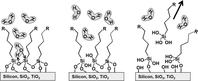
FIGURE 13.2 Hydrolytic instability of siloxane-based monolayers due to penetration of water and other reactive species to the organic-inorganic interface.
13.2.3 Phosphonic Acids
Phosphonic acids and their salts can bind strongly to many surfaces [39–45]. White it is widely recognized that the alkylsilane chemistry requires –OH groups to proceed, evidence suggests that the phosphonic acid chemistry on silicon can occur without surface –OH groups [43]. Since metal oxides such as silicon and TiO2 often have bridging oxygens (like that shown in Fig. 13.1b), the ability to graft in the absence of water or hydroxyls may provide a more reproducible method of attachment, avoiding the solution-phase hydrolysis that causes clumping of organosilanes. XPS studies have indicated that the binding is tridentate [45]. This approach has been successfully used to graft cell-binding proteins to titanium surfaces [40] and as a starting point for linking proteins to TiO2 via nonspecific interactions with the ammonium dodecyl phosphate [46].
13.2.4 Alkene Grafting
Because of the irreproducibility and hydrolytic instability of the organosilicon chemistry, substantial efforts have been made to eliminate the need for a surface oxide altogether, by using alternative reactions to form direct silicon–carbon linkages. The goal of a direct Si–C linkage was motivated by the fact that hydrolysis reactions are often driven by strongly polar bonds; for example, Si–O–Si (silica, silicones) and C–O–C (ether) bonds are more resistant to hydrolysis than Si–O–C bonds. Similarly, chemical compounds containing direct Si–C bonds are much more resistant to hydrolysis than those with Si–O–C linkages [47]. These factors all suggest that bonding organic layers directly to the silicon surface without intervening oxygen atoms may yield improved stability, as well as possibly providing a more electronically conductive interface. Working directly on silicon also allows one to take full advantage of the fact that wet chemical etching using NH4F forms extraordinarily flat Si(111) surfaces with all exposed silicon “dangling bonds” terminated with H atoms [48], providing an almost perfectly homogeneous starting surface. While the Si(001) surface is used almost exclusively in microelectronics processing, the Si(111) surface is generally preferred for biological studies. This difference arises primarily because Si(111) surfaces can be easily prepared with atomic flatness due to the highly anisotropic nature of the NH4F chemical etch [48,49].
The “H-terminated” silicon surface produced by NH4F etching is moderately reactive but can be handled in air for very short periods of time, enabling one to use benchtop chemistry for subsequent chemical functionalization. Most reactions on H-terminated silicon have used terminal alkenes. The reaction of alkenes with H-terminated silicon is not spontaneous, but must be activated. Linford et al. showed that terminal alkenes can be thermally activated to link directly to the silicon surface [50,51]. Additional studies have shown that the reaction can be activated using radical initiators to remove a surface H atom (thereby creating a reactive Si “dangling bond”) [50,51], or by using energetic photons, typically at 254 nm [52–56].
Figure 13.3 outlines the procedure typically used for photochemical grafting of alkenes onto H-terminated Si surfaces [52–56]. Studies using X-ray photoelectron spectroscopy (XPS) and Fourier transform infrared spectroscopy (FTIR) show that in most cases the grafting reactions are self-limiting, stopping after a coverage of approximately one monolayer, although multilayer formation is possible in some cases [57,58]. While initial studies of alkene grafting focused primarily on simple alkenes, the range of opportunities expands greatly using bifunctional molecules [52–54,59–64]. Sieval et al. showed these grafting methods could be extended to enable multistep surface chemical synthesis by using ω-functionalized 1-alkenes; however, because many functional groups of interest react directly with silicon (including both amines and carboxylic acids), it is necessary to use protecting groups [61]. The use of protecting groups is complicated because care must also be exerted in the choice of deprotection conditions to ensure that the harsh chemicals do not etch the underlying silicon or the Si–C bonds. Additionally, since the protecting groups are sometimes larger than the size of the alkyl chain, the protecting groups can inhibit good packing of the molecules on the surface, resulting in a molecular layer that has poor stability in aqueous media. Figure 13.3b illustrates some of the molecules that have been grafted successfully [53,54,65,66]. They include pure alkenes and molecules bearing additional functional and/or protecting groups. For example, TFAAD and tBoc contain protected amine groups and thereby provide routes to amine-terminated surfaces. The molecule with the dmt (dimethoxytrityl) group can be deprotected to yield alcohol-terminated surfaces [65], while UAME (undecylenic acid methyl ester) is an excellent route to carboxylic acid-modified surfaces, and oligomers of ethylene glycol form protein-resistant surfaces [66,67]. This combination of molecules provides many different pathways for linking DNA, proteins, and other biomolecules to the surface.
While most studies of alkene grafting have been performed on group IV semiconductors, alkenes will also photochemically graft to metal oxides such as TiO2 [58,68,69].
13.3 DNA-MODIFIED SEMICONDUCTOR SURFACES
13.3.1 DNA-Modified Silicon
One attractive feature of DNA chemistry is that automatic DNA synthesizers make it simple to produce DNA oligonucleotides terminated with reactive terminal groups. While termination with amine groups is common, one difficulty in this approach is that primary amines are also reactive with atmospheric CO2. Consequently, many studies have instead used DNA terminated with thiol (–SH) groups. This approach has the additional advantage that the surface linkage can be facilitated using heterobifunctional cross-linkers such as sulfosuccinimidyl 4-(N-maleimidomethyl)cyclohexane 1-carboxylate (Sulfo-SMCC), which has one functional group (N-hydroxysuccinimide) that reacts with primary amines to form amide linkages and a second group (maleimide) that will link to sulfhydryl (thiol, –SH) groups. Figure 13.4 depicts this overall pathway on silicon. We note that because the linkers are often larger than the alkyl chains of the underlying functionalization layer (and the DNA molecules larger yet), after SSMCC there are likely unreacted but inaccessible amine groups remaining, and after linking of DNA there are likely unreacted maleimide groups as well. Because each successive step in this multistep pathway involves molecules of increasing size, there are often advantages in using initial functionalization layers in which molecules having chemically unreactive terminal groups (such as EG3 or EG6 depicted in Fig. 13.3b, which resist protein binding) are mixed with molecules having reactive end groups (such as TFAAD) that will serve as covalent attachment points. Making such mixed layers can reduce the undesired effects of unreacted but inaccessible functional groups and can aid in making the surfaces resistant to nonspecific binding while retaining their ability to react with specific biomolecular targets of interest [66].
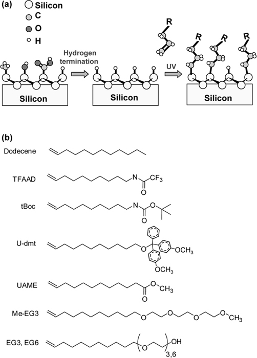
FIGURE 13.3 (a) Alkene grafting to H-terminated surfaces of silicon. (b) Summary of some of the bifunctional alkenes that have been grafted to silicon surfaces.
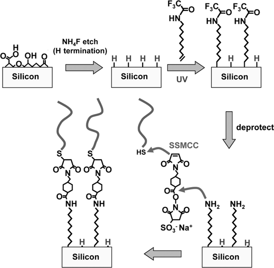
FIGURE 13.4 Overall summary of pathway to DNA-modified silicon surface.
Making mixed layers can also enhance the reactivity of the remaining surface attachment points due to steric blocking that can occur in dense molecular layers. For example, Bocking et al. prepared layers by thermal hydrosilylation of 10-undecenoic acid and then linked peptides to the surface by first using 1-ethyl-3-[3-dimethyla-minopropyl]carbodiimide (EDC) followed by N-hydroxysuccinimide (NHS) to produce a NHS–terminated surface, which was then reactive toward a simple tripeptide. They found that at high coverages the exposed carboxylic acid groups were difficult to activate. This behavior might arise from strong hydrogen bonding between adjacent molecules. Yet, if the hydrosilylation reaction was terminated early, the samples showed significant levels of oxidation that led to mechanical failure of the devices due to dissolution of the underlying nanostructured Si [70].
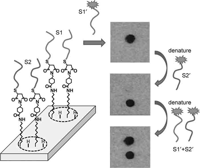
FIGURE 13.5 Testing selectivity and reversibility of hybridization of DNA oligonucleotides covalently grafted onto the Si(001) surface. Figure adapted from Ref. 53.
Figure 13.5 depicts data showing the interaction of a DNA-modified Si surface with complementary and noncomplementary DNA targets in solution. In this case, the surface was linked to two different sequences, S1 and S2, in two spots on the surface. The samples were then covered with a fluorescently labeled complement, S1′, and the fluorescence measured. The images in Fig. 13.5 are negatives, so that the dark region corresponds to high fluorescence intensity. Figure 13.5 shows that sequence S1′ binds to the surface region functionalized with S1 but not to the surface reaction functionalized with sequence S2, which is a 4-base mismatch (out of 16) to S1. To test the reversibility of binding, the sample was then denatured and exposed to a fluorescently labeled complement to S2 (labeled as S2′), and in this case the other surface region shows high fluorescence intensity (dark in the image). Finally, the sample was denatured and exposed to a mixture of both targets. These and other studies show that surfaces of semiconductors such as silicon can be functionalized with DNA in a manner that gives excellent selectivity, even able to detect a single-base mismatch [71]. With sufficiently densely packed layers, repetitive hybridization–denaturation cycles can yield losses of approximately 1% per cycle. This value is sufficiently low that silicon can be used as a high-quality substrate for interfacing DNA and other biomolecules to surfaces.
The selectively DNA-modified surfaces can be evaluated by comparing the bonding of surface-tethered oligonucleotides with molecules in solution having complementary and noncomplementary DNA sequences. One of the most important goals is to be able to distinguish between perfectly complementary sequences and those having mismatches of a single base. These so-called single nucleotide polymorphisms (SNPs) are believed to be important in factors underlying the genetic basis of disease [72,73]. Discriminating between perfect matches and single-base mismatch has been achieved at silicon surfaces using fluorescence [71] and electrochemical [74] methods.
One of the primary motivations for interfacing biomolecules to semiconductors such as silicon is to take advantage of the unique electronic properties of semiconductors to make high-sensitivity devices such as transistors, which are essentially charge amplifiers. Devices of this type have been made from silicon for many years, but have not found widespread applications in large part because they suffer from chemical and electrical instability due to the factors discussed above. In addition, while studies on silicon demonstrate the benefits of using photochemical grafting to prepare complex interfaces the utility of silicon in aqueous environments is limited by the fact that penetration of water to the interface hydrolyzes Si–C and Si–O–C bonds, eventually removing the molecular layers from the substrate. This process can be slowed by using hydrophobic alkyl chains, but ultimately the molecular layers formed on silicon are only kinetically stable. To make truly ultrastable molecular layers, a different approach is necessary, starting with materials having greater intrinsic stability.
13.3.2 DNA-Modified Diamond
Carbon-based materials are of great interest in part because the properties can be controlled by varying the hybridization [75]. Diamond is of particular interest because in addition to having outstanding mechanical and optical properties, it is a semiconductor, having a bandgap of 5.5 eV. Diamond's semiconducting properties enable the creation of hybrid bioelectronic devices such as biologically actuated field-effect transistors, or “bio-FETs” [76]. While diamond in bulk form remains prohibitively expensive for most practical applications, thin diamond coatings < 1 μm in thickness can be easily and inexpensively deposited on a wide range of materials including metals, silicon, and transparent quartz; these diamond films yield the chemical stability of diamond in a practical and scalable manner. Amorphous carbon and “diamond-like” carbons with mixed sp2–Sp3 hybridization can also be deposited as thin-film coating materials that facilitate integration with a wider range of other materials [75,77,78].
Carbon surfaces are typically cleaned using atomic hydrogen from a hydrogen plasma, yielding “H-terminated” surfaces [79]. H-terminated diamond is very reproducible and stable even in air. However, this high stability also makes H-terminated diamond surfaces difficult to functionalize. One approach to diamond functionalization is the use of aryldiazonium salts, as depicted in Fig. 13.1e [80–83]. Nitrobenzenediazonium salts can be reduced to make amine-terminated diamond surfaces, enabling coupling chemistry like that depicted above for silicon to be applied to diamond [82,83].
A more versatile approach for modifying diamond has been to use photochemical grafting of organic alkenes. The procedure for carrying out the photochemical grafting is similar to that on silicon described earlier (see below), the only notable difference being the initial cleaning process to make the diamond surface chemically uniform, with all exposed surface bonding linked to hydrogen atoms. This H-terminated diamond is typically made by exposing the diamond sample to a hydrogen plasma [79]. The H-terminated diamond is covered with a thin film of suitable reactant and then illuminated with ultraviolet light, typically at 254 nm for ~12 h [84,85]. Using the TFAAD molecule shown in Fig. 13.3b, DNA-modified diamond samples were prepared using chemistry similar to that shown for silicon.
The outstanding properties of diamond as a robust substrate for functional surfaces are apparent from the greatly increased stability of DNA on diamond compared with other substrates, as shown in Fig. 13.6 [85]. In this comparison, several different substrates were modified with organic molecules terminating in a primary amine group. These amine groups were then linked to thio-modified DNA oligonucleotides using the heterobifunctional linker SSMCC. The stability and selectivity of the resulting DNA-modified surfaces were then evaluated by exposing the DNA-modified diamond surfaces to repeated cycles of hybridization and denaturation using fluorescently labeled targets with complementary and noncom-plementary sequences [85]. In addition to the DNA-modified diamond, the graph shows data for surfaces produced from commercial amine-modified glass slides (Corning GAPS II), amine-terminated self-assembled monolayers on gold, and surfaces prepared by photochemically grafting molecular layers to H-terminated Si(111) and to H-terminated glassy carbon. All of these examples started with amine-terminated molecular layers and then used identical DNA chemistry. Consequently, they have identical molecular structures except for the two atoms (labeled “A” and “B” in Fig. 13.6a) that form the molecule-substrate interface.
Figure 13.6b shows that the two carbon substrates—diamond and glassy carbon—clearly exhibit superior stability. These results particularly highlight the importance of the substrate-to-molecule bond in controlling the overall stability of biomolecular interfaces, as the extraordinary stability of the C–C bond at the interface provides unprecedented chemical stability to the biomolecular layers.
13.3.3 DNA on Metal Oxides
Recent studies showed that alkenes will graft to surfaces of TiO2 and other metal oxides [58,69], presumably linking via surface –OH groups. Using the TFAAD molecule depicted in Fig. 13.3b, DNA-modified TiO2 surfaces were prepared using TFAAD, deprotecting, and using SSMCC as a linker [69]. Figure 13.7 shows some of the results obtained with two different oligonucleotides. Tests of the stability in repeated cycles of hybridization and denaturation showed that the surfaces have good stability, although not as stable as DNA on diamond. In this particular case, the Ti–O–C linkages at the surface are likely susceptible to hydrolysis, so that the molecular layer stability hinges on having some partial cross-linking of TFAAD on the surface. Nevertheless, TiO2 is an attractive material for some applications because Ti metal can be easily deposited onto a wide range of materials (including polymers), potentially facilitating the integration of DNA and other biomolecules with polymers and other materials.
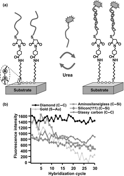
FIGURE 13.6 Comparison of stability in repeated cycles of hybridization and denaturation of several different materials. In each case, the sample was functionalized to produce an amine-terminated surface, followed by identical methods of covalent grafting of thio-modified DNA to the surface. The samples were subjected to repeated cycles of hybridization with a fluorescently labeled complementary sequence, followed by denaturation in 8.3 M urea. The different absolute signal intensities at the start of the experiment are a consequence of the different optical properties of the materials and have no important consequence. Note the excellent stability of diamond and glass carbon in comparison with the other materials. Figure adapted from Ref. 85.
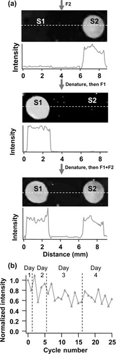
FIGURE 13.7 DNA hybridization on DNA-modified TiO2 surface prepared by photochemical grafting of TFAAD to TiO2. Two surface regions were modified with two different oligonucleotides (S1 and S2), each having a 16-base hybridization region and different from one another by 4 bases. Fluorescence images and intensity profiles are shown after exposure to the fluorescently labeled complements F2 (fluorescent complement to S2) and F1 (fluorescence complement to S1). Figure adapted from Ref. 69.
13.4 PROTEINS AT SURFACES
13.4.1 Protein-Resistant Surfaces
One of the biggest challenges in working with biological systems is that many proteins undergo nonspecific adsorption on surfaces. This nonspecific adsorption is often accompanied by denaturation of the proteins and leads to a variety of undesired consequences, including fouling of biosensors and generation of an inflammatory response. The use of such short-chain ethylene glycol (EG) oligomers to reduce nonspecific binding has been well established in studies of self-assembled monolayers on gold [86–90] and can also be applied to semiconductors such as silicon and diamond [66,67,91]. As depicted in Fig. 13.8a, alkenes with terminal EG groups effectively repel nonspecific binding, even when as few as three EG groups are present (as in Fig. 13.8a). Longer oligomers such as EG6 are even more effective. By making mixed monolayers incorporating EG oligomers and molecules having reactive functional groups (such as TFAAD), the overall selectivity of the surface toward the target of interest can be maximized [67].
Figure 13.8b depicts data for nanocrystalline diamond films modified with four different surface treatments, interacting with four different proteins; these data show that even short oligomers such as EG6 are highly effective at reducing nonspecific binding of proteins [66,67]. Grafting of the EG6 oligomers reduces the nonspecific binding of avidin on nanocrystalline diamond to less than 0.02 monolayer [67], a level similar to that observed with self-assembled monolayers on gold [87].
XPS studies can also be useful in identifying protein adsorption in a quantitative manner. For example, Fig. 13.8c shows XPS data for an EG6-functionalized diamond surface and a H-terminated diamond surface, both shown before and after exposure to fibrinogen in solution. An XPS spectrum of a drip-dried film of fibrinogen is also shown. The presence of the fibrinogen can be inferred from the presence of an N 1s peak in the XPS spectrum of the H-terminated diamond after immersion in fibrinogen. However, there is no detectable N 1s or S 2p for the EG6-modified sample. Based on the signal-to-noise ratio of the experiments, from these data we infer that the EG6 monolayer reduces the nonspecific binding of fibrinogen by >97%. Both XPS and fluorescence methods show that diamond surfaces modified with EG oligomers have superior stability to those made on silicon or gold. Figure 13.9 shows fluorescence measurements testing the ability of EG-modified surfaces of silicon, gold, and diamond to resist the nonspecific binding of avidin over longer periods of time. While at short times silicon is the best (likely because of its atomically flat structure), over a period of 10 days in water both the silicon and gold surfaces degrade, while the EG-modified diamond surface retains its ability to resist nonspecific binding. Corresponding XPS measurements showed no significant change in the surface chemistry of EG-modified diamond [66]. In contrast, EG-modified silicon and gold samples both exhibited significant increases in nonspecific binding and evidence for partial loss of the EG layers [66,67,87,91].
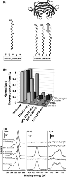
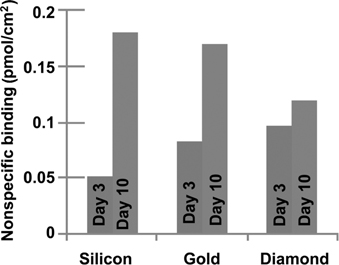
FIGURE 13.9 Time-dependent changes in the ability of EG layers on silicon, gold, and diamond to resist nonspecific binding of avidin. Note that while functionalized silicon is best at short times, the stability of diamond allows the molecular functionalization layers to persist for long periods of time and therefore retains its effectiveness for longer periods of time. Figure adapted from Ref. 66.
13.4.2 Protein-Selective Surfaces
Just as DNA can be used to link to its complementary sequence, proteins are often able to recognize specific molecules. The ability to functionalize semiconductor surfaces with proteins, particularly antibodies, is of interest for many applications in sensing, medical diagnostics, and the rapidly growing field of proteomics.
Antibodies contain two major domains: the Fab region is primarily responsible for biomolecular recognition, while the Fc region is rich in carboxylic acid groups. Unfortunately, existing chemistries are better suited to linking to the antibody's amine groups than to the carboxylic acid groups. Existing biochips often use Protein G to selectively immobilize antibodies via the Fc region, but this does not provide the type of strong, covalent attachment desired. Consequently, linking through the amine groups in the Fab region is a reasonable, albeit less than ideal compromise. Hartl et al. covalently linked proteins to diamond using succinic anhydride to convert the amine-terminated surface to a carboxylic acid-modified surface, and then using EDC and NHS to link to the amine groups of two different proteins: green fluorescent protein (GFP) and the catalase enzyme [92]. Their work demonstrated that it is possible to make highly robust protein interfaces to diamond that retained their biological activity. Figure 13.10 illustrates another pathway toward antibody-modified surfaces, using glutaraldehyde to couple between amine-terminated surfaces and the amine groups of the antibody. This approach has been used to make antibody-selective surfaces on diamond and has also been used to make cell-selective surfaces [91]. By linking E. coli antibodies to a diamond surface, it is possible to selectively capture E. coli cells. This may provide an important opportunity for detection of biological pathogens via continuous monitoring.
![]()
FIGURE 13.8 Nonspecific binding of proteins at semiconductor surfaces. (a) Use of alkenes terminated with ethylene glycol groups to make protein-resistant surfaces on silicon and diamond. (b) Comparison of different mixed layers to resist nonspecific binding of avidin. Figure adapted from Ref. 66. (c) XPS measurements of H-terminated and EG6-terminated diamond, before and after exposure to fibrinogen. Note that immersion into fibrinogen leads to large N 1s and S 2p peaks on the H-terminated sample, but no detectable change on the EG6-modified sample. This establishes that the EG layer is very effective at resisting nonspecific binding of fibrinogen. Figure adapted from Ref. 91.
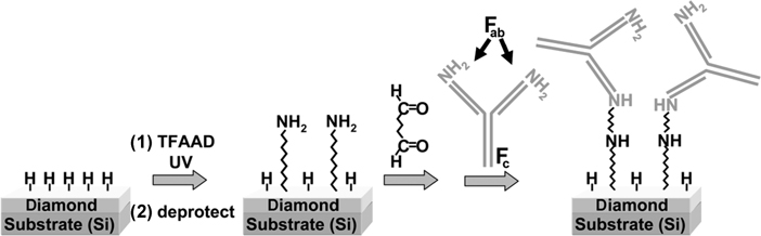
FIGURE 13.10 One scheme for linking antibodies to semiconductor surfaces via the Fab region.
The ultimate measure of the selectivity of biomolecular interface is the ratio of specific binding (binding of a particular target molecule in solution) to nonspecific binding. By making mixed monolayers in which molecules bearing a reactive group of interest (such as a protected amine for subsequent modification) are distributed among EG oligomers, the overall ratio of specific to nonspecific binding (S/NS ratio) can be significantly improved. Experimental measurements using the biotin-avidin system showed that the monolayers formed using ~ 10% of a protected amine in 90% of ethylene glycol in the parent liquid yielded the best overall selectivity; these surfaces were able to selectively bind avidin even in undiluted chicken serum [67]. These experiments demonstrate that multiple properties can be optimized using mixed monolayers.
13.5 COVALENT BIOMOLECULAR INTERFACES FOR DIRECT ELECTRICAL BIOSENSING
13.5.1 Detection Methods on Planar Surfaces
One of the most intriguing applications of biomolecular surface chemistry on semiconductors is the potential development of label-free schemes to convert biological information directly into electrical signals [6,7,11,22,76,93–100]. The basis for semiconductor-based sensing schemes is that the conductivity of semiconductors can be very sensitive to the presence of small charges at or near the semiconductor surfaces. Under appropriate conditions (ones that, unfortunately, are extremely difficult to achieve in aqueous media), some transistors are even able to detect the charge of a single electron [101]. In biological applications, the essential idea is that biomolecules, ions, and other charged species located near the surface of the semiconductor create electric fields that penetrate a short distance (typically 10–1000 nm) into the semiconductor bulk. These penetrating electric fields repel and attract charge carriers consisting of negatively charged electrons in the conduction band and positively charged “holes” (electron vacancies) in the valence band, thereby changing the conductivity of the semiconductor in the region closest to the solid-liquid interface. These changes in conductivity can be measured perpendicular to the interface (between the bulk semiconductor and an electrode in the adjacent liquids phase) or parallel to the interface by using two electrical contacts on the semiconductor surface, as depicted in Fig. 13.11.
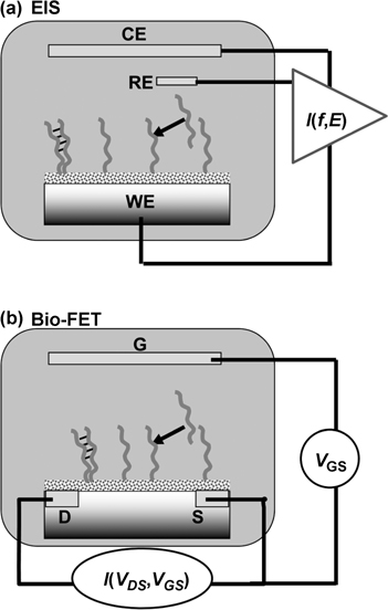
FIGURE 13.11 Two methods for achieving electrical detection of biological binding events at functionalized semiconductor surfaces. (a) Electrochemical impedance spectroscopy, measuring the current as a function of frequency (f) and the electrochemical potential (E) in a three-electrode potentiostat geometry. (b) Biologically sensitive field-effect transistor (bio-FET), measuring the drain-source current as a function of the drain-source voltage and the gate-source voltage.
In the former technique, the electrical impedance perpendicular to the interface is measured using a technique known as electrochemical impedance spectroscopy (EIS). EIS measures the amplitude and phase shift of the current flow induced by a sinusoidally modulated voltage applied using the sample as the working electrode in a three-electrode electrochemical cell, as depicted in Fig. 13.11a [7,8,11]. The EIS data are frequency-dependent complex numbers that are often plotted as figures in the complex plane and sometimes fit to electrical circuit models to extract parameters such as the interfacial capacitance and solution resistance.
Measurements parallel to the surface typically involve a configuration like a field-effect transistor (FET), as in Fig. 13.11b. Two electrodes (referred to as the “source” and “drain” electrodes) are placed on the sample and used to measure the conductivity parallel to the interface; a third electrode (typically an in-solution reference electrode) can be used to adjust the initial state, or “operating point” of the transistor for maximum sensitivity [22,93,94,96,102,103]. The current between source and drain is then measured as a function of the drain–Source voltage and the gate–Source voltage.
The FET configuration requires deposition of contacts directly onto the front of the sample and can suffer from leakage current through the adjacent liquid, but can be more sensitive. The EIS configuration conveniently requires only one electrical contact that can be made to the back of the sample, but the resistance of the bulk substrate becomes incorporated into the measurement. Both EIS and FET measurements are strongly dependent on the proximity of the biomolecule to the semiconductor, since both measure the change in impedance in the semiconductor space-charge region that is induced by the biomolecular charge.
Figure 13.12 shows EIS data for DNA grafted onto n-type (a) and p-type (b) silicon after exposure to a complementary sequence, after denaturing, and after exposure to a noncomplementary sequence [11]. Binding of DNA significantly increases the impedance on the n-type sample and decreases the impedance on the p-type sample. This can be easily explained using the fact that on n-type substrates the charge carriers are electrons; the negatively charged DNA repels these electrons from the near-surface region, leaving it more highly resistive. In contrast, on p-type substrates the charge carriers are holes; the negatively charged DNA attracts these holes to the surface and increases the conductivity. With positively charged molecules, the situation reverses. Thus, from a knowledge of the doping of the semiconductor the charge of the binding molecule can be inferred. Indeed, measurements using positively charged human IgG antibodies showed just such a reversal [99].
13.5.2 Sensitivity Considerations
A critical factor controlling the sensitivity of bioelectronic sensing systems is that the distribution of charges in an ionic medium leads to a characteristic length scale, the Debye length, which represents the distance over which a locally varying electrostatic field (due to a charged biomolecule or surface) drops to 1/e of its initial value.
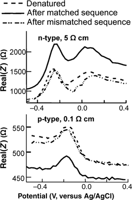
FIGURE 13.12 Electrochemical impedance spectroscopy measurements of DNA-modified silicon surfaces after exposure to complementary (matched) sequence and noncomplementary (mismatched) sequence. Data are shown on both n-type and p-type silicon samples. Binding of the negatively charged DNA molecule to its surface-bound complement increases the impedance on n-type samples and decreases the impedance on p-type samples. Figure adapted from Ref. 11.
The Debye length is given by
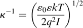
where κ−1 is the Debye length, ε0 is the permittivity of free space, ε is the permittivity of the aqueous medium, and q is the electron charge. I=Σiciz2i is the ionic strength, with ci and zi representing the concentration and charge of each species present. At physiological salt concentrations, the Debye length is very short, approximately 0.8 nm. Consequently, in order to have high sensitivity it is crucial for the biological species to be linked very close to the semiconductor surface [6,104]. While in principle the sensitivity can be enhanced by using lower ionic strength solutions (and thereby extending the Debye length), most biomolecular interactions in nature take place in high ionic strength environments and working in low ionic strength solutions can alter these interactions. However, a compromise can be reached, using salt concentration on the order of 10 mM, yielding a Debye length of ~ 3nm [6,104]. While the requirements to achieve high sensitivity in bio-to-electronic transduction are daunting, clever approaches to achieving the transduction continue to emerge. For example, Fritz et al. detected DNA at nanomolar concentrations by using two sensors in parallel and measuring the difference between them [74]. In this case, many causes of drift (such as temperature changes) are effectively nulled out, allowing more sensitive detection of the DNA hybridization events [74].
The above discussion is necessarily incomplete, and the interested reader is referred to more thorough quantitative analyses of surface charge distributions [6,7,74,93,104,105]. However, several points are immediately clear: First, that to achieve maximum sensitivity it is crucial to have the molecular layers as short as possible. Second, the performance is also strongly dependent on the quality of surface and in particular the nature, energy, and stability of electronic states at the surface.
13.6 NANOWIRE SENSORS
The ability to prepare silicon and other semiconductors as one-dimensional nanowires brings with it opportunities for new types of chemical biological sensors. A number of recent studies have fabricated silicon-based biosensors using Si nanowires [10,106,107]. Li et al. [107] made label-free DNA sensors using planar Si nanowires that were oxidized to produce a ~ 3 nm thick SiO2 coating, followed by the use of silane chemistry. Cui et al. argued that it should be possible to achieve single-molecule detection [10]. For example, Li et al. linked short DNA oligonu-cleotides (12-mers) to silicon nanowires using silane chemistry [107]. By measuring the nanowire conductance and the surface photovoltage effect, they succeeded in obtaining a sensitivity of 25 pM. Moreover, they were able to easily distinguish between perfectly complementary sequences and single-base mismatches. One of the key potential advantages of nanowire sensors is that the nanowires are smaller than the thickness of the semiconductor space-charge region. Consequently, nanowire sensors might be expected to have a larger fractional change in conductivity compared with larger planar sensors. However, because of the small size of the nanowires the currents involved are very small, and great care must be taken to ensure that the measured signals arise from binding to the nanowire surface rather than to the contacts or other exposed surfaces. Additionally, while high sensitivity can be achieved, the small size of the sensor also makes the effective capture volume very small. Yet, this remains an intense area of continued activity.
13.7 SUMMARY
Covalently grafted molecular layers on semiconductors provide the opportunity to create highly stable, functional interfaces. The overall utility of these layers is often connected to their long-term stability, driving a desire for increasingly robust interfaces. Silicon, long the foundation of microelectronics, is very useful for short-term studies and is readily available, inexpensive, and can be easily processed using standard techniques of microelectronics processing. However, new applications such as environmental sensing, homeland security, and detection of water-borne pathogens continue to lead to the development of more robust materials able to withstand use for long periods of time. Thin-film diamond is one of the attractive candidates because of its outstanding mechanical properties and chemical stability. The successful integration of biological molecules with diamond, silicon, and semiconductor materials in a manner that takes advantage of the unique electronic properties of these materials is difficult, but holds great promise for new and emerging applications in chemical and biological sensing and biomedical diagnostics.
ACKNOWLEDGMENTS
The work described here was supported in part by the National Science Foundation Grants CHE-0314618, CHE-0613010, CHE-0911543, DMR-0210806, and DMR-0706559. The authors acknowledge fruitful collaborations and interactions with Dr. James Butler and Professor Lloyd M. Smith throughout this work.
REFERENCES
1. Castner, D. G.; Ratner, B. D. Surf. Sci. 2002, 500(1–3), 28.
2. Nuzzo, R. G.; Dubois, L. H.; Allara, D. L. J. Am. Chem. Soc. 1990, 112, 558.
3. Nuzzo, R. G.; Allara, D. L. J. Am. Chem. Soc. 1983, 105(13), 4481.
4. Laibinis, P. D.; Whitesides, G. M.; Allara, D. L.; Tao, Y.-T.; Parikh, A. N.; Nuzzo, R. G. J. Am. Chem. Soc. 1991, 113, 7152.
5. Bergveld, P. IEEE Trans. Biomed. Eng. 1970, 17, 70.
6. Bergveld, P. Biosens. Bioelectron. 1991, 6(1), 55.
7. Souteyrand, E.; Cloarec, J. P.; Martin, J. R.; Wilson, C.; Lawrence, I.; Mikkelsen, S.; Lawrence, M. F. J. Phys. Chem. B 1997, 101(15), 2980.
8. Souteyrand, E.; Martin, J. R.; Martelet, C. Sens. Actuators B 1994, 20, 63.
9. Beebe, D. J.; Mensing, G. A.; Walker, G. M. Annu. Rev. Biomed. Eng. 2002, 4, 261.
10. Cui, Y.; Wei, Q. Q.; Park, H. K.; Lieber, C. M. Science 2001, 293(5533), 1289.
11. Cai, W.; Peck, J. R.; van der Weide, D. W.; Hamers, R. J. Biosens. Bioelectron. 2004, 19(9), 1013.
12. Kar, S.; Miramond, C.; Vuillaume, D. Appl. Phys. Lett. 2001, 78(9), 1288.
13. Casey, W. H.; Lasaga, A. C.; Gibbs, G. V. Geochim. Cosmochim. Acta 1990, 54(12), 3369.
14. Sjoberg, S. J. Non-Cryst. Solids 1996, 196, 51.
15. Chazalviel, J. N. J. Phys. IV 1994, 4(C1), 117.
16. Watanabe, S. Surf. Sci. 1995, 341(3), 304.
17. Fukidome, H.; Pluchery, O.; Queeney, K. T.; Caudano, Y.; Raghavachari, K.; Weldon, M. K.; Chaban, E. E.; Christman, S. B.; Kobayashi, H.; Chabal, Y. J. Surf. Sci. 2002, 502, 498.
18. Shimojima, A.; Sugahara, Y.; Kuroda, K. Bull. Chem. Soc. Jpn. 1997, 70(11), 2847.
19. Tada, H.; Nagayama, H. Langmuir 1995, 11(1), 136.
20. Morita, M.; Ohmi, T.; Hasegawa, E.; Kawakami, M.; Ohwada, M. J. Appl. Phys. 1990, 68 (3), 1272.
21. Weldon, M. K.; Queeney, K. T.; Chabal, Y. J.; Stefanov, B. B.; Raghavachari, K. J. Vac. Sci. Technol. B 1999, 17(4), 1795.
22. Uno, T.; Tabata, H.; Kawai, T. Anal. Chem. 2007, 79(1), 52.
23. Netzer, L.; Iscovici, R.; Sagiv, J. Thin Solid Films 1983, 100(1), 67.
24. Netzer, L.; Iscovici, R.; Sagiv, J. Thin Solid Films 1983, 99(1–3), 235.
25. Ulman, A. Adv. Mater. 1990, 2(12), 573.
26. Brzoska, J. B.; Benazouz, I.; Rondelez, F. Langmuir 1994, 10(11), 4367.
27. Fadeev, A. Y.; McCarthy, T. J. Langmuir 2000, 16(18), 7268.
28. Faucheux, N.; Schweiss, R.; Lutzow, K.; Werner, C.; Groth, T. Biomaterials 2004 25(14), 2721.
29. Halliwell, C. M.; Cass, A. E. G. Anal. Chem. 2001, 73(11), 2476.
30. Kallury, K. M. R.; Krull, U. J.; Thompson, M. Anal. Chem. 1988, 60(2), 169.
31. Chrisey, L. A.; Lee, G. U.; O'Ferrall, E. O. Nucleic Acids Res. 1996, 24, 3031.
32. Ulman, A. Chem. Rev. 1996, 96(4), 1533.
33. Angst, D. L.; Simmons, G. W. Langmuir 1991, 7(10), 2236.
34. Wasserman, S. R.; Tao, Y. T.; Whitesides, G. M. Langmuir 1989 5(4), 1074.
35. Dugas, V.; Chevalier, Y. J. Colloid Interface Sci. 2003, 264(2), 354.
36. Steinem, C.; Janshoff, A.; Lin, V. S. Y.; Volcker, N. H.; Ghadiri, M. R. Tetrahedron 2004, 60(49), 11259.
37. Olmos, D.; Gonzalez-Benito, J.; Aznar, A. J.; Baselga, J. J. Mater. Process. Technol. 2003, 143, 82.
38. Cypryk, M.; Apeloig, Y. Organometallics 2002, 21(11), 2165.
39. Adadi, R.; Zorn, G.; Brener, R.; Gotman, I.; Gutmanas, E. Y.; Sukenik, C. N. Thin Solid Films 2009 518(8), 1966.
40. Danahy, M. P.; Avaltroni, M. J.; Midwood, K. S.; Schwarzbauer, J. E.; Schwartz, J. Langmuir 2004, 20(13), 5333.
41. Gawalt, E. S.; Avaltroni, M. J.; Koch, N.; Schwartz, J. Langmuir 2001, 17(19), 5736.
42. Helmy, R.; Fadeev, A. Y. Langmuir 2002, 18(23), 8924.
43. Hanson, E. L.; Schwartz, J.; Nickel, B.; Koch, N.; Danisman, M. F. J. Am. Chem. Soc. 2003, 125(51), 16074.
44. Gawalt, E. S.; Avaltroni, M. J.; Danahy, M. P.; Silverman, B. M.; Hanson, E. L.; Midwood, K. S.; Schwarzbauer, J. E.; Schwartz, J. Langmuir 2003, 19(1), 200.
45. Gouzman, I.; Dubey, M.; Carolus, M. D.; Schwartz, J.; Bernasek, S. L. Surf. Sci. 2006, 600(4), 773.
46. Blattler, T. M.; Binkert, A.; Zimmermann, M.; Textor, M.; Voros, J.; Reimhult, E. Nanotechnology 2008, 19(7)
47. Crandall, J. K.; Morelfourrier, C. J. Organomet. Chem. 1995, 489(1–2), 5.
48. Dumas, P.; Chabal, Y. J.; Jakob, P. Surf. Sci. 1992, 269, 867.
49. Jakob, P.; Chabal, Y. J. J. Chem. Phys. 1991, 95(4), 2897.
50. Linford, M. R.; Fenter, P.; Eisenberger, P. M.; Chidsey, C. E. D. J. Am. Chem. Soc. 1995, 117, 3145.
51. Linford, M. R.; Chidsey, C. E. D. J. Am. Chem. Soc. 1993, 115, 12631.
52. Cicero, R. L.; Linford, M. R.; Chidsey, C. E. D. Langmuir 2000, 16, 5688.
53. Strother, T.; Hamers, R. J.; Smith, L. M. Nucleic Acids Res. 2000, 28(18), 3535.
54. Strother, T.; Cai, W.; Zhao, X.; Hamers, R. J.; Smith, L. M. J. Am. Chem. Soc. 2000, 122(6), 1205.
55. Stewart, M. P.; Buriak, J. M. J. Am. Chem. Soc. 2001, 123(32), 7821.
56. Stewart, M. P.; Buriak, J. M. Angew. Chem., Int. Ed. 1998, 37(23), 3257.
57. Colavita, P. E.; Sun, B.; Tse, K. Y.; Hamers, R. J. J. Am. Chem. Soc. 2007, 129(44), 13554.
58. Franking, R. A.; Landis, E. C.; Hamers, R. J. Langmuir 2009, 25(18), 10676.
59. Sieval, A. B.; Vleeming, V.; Zuilhof, H.; Sudholter, E. J. R. Langmuir 1999, 15(23), 8288.
60. Sieval, A. B.; Linke, R.; Heij, G.; Meijer, G.; Zuilhof, H.; Sudholter, E. J. R. Langmuir 2001, 17(24), 7554.
61. Sieval, A. B.; Demirel, A. L.; Nissink, J. W. M.; Linford, M. R.; van der Maas, J. H.; de Jeu, W. H.; Zuilhof, H.; Sudholter, E. J. R. Langmuir 1998 14(7), 1759.
62. Boukherroub, R.; Wojtyk, J. T. C.; Wayner, D. D. M.; Lockwood, D. J. J. Electrochem. Soc. 2002, 149(2), H59.
63. Boukherroub, R.; Wayner, D. D. M. J. Am. Chem. Soc. 1999, 121(49), 11513.
64. Boukherroub, R.; Morin, S.; Bensebaa, F.; Wayner, D. D. M. Langmuir 1999, 15(11), 3831.
65. Pike, A. R.; Lie, L. H.; Eagling, R. A.; Ryder, L. C.; Patole, S. N.; Connolly, B. A.; Horrocks, B. R.; Houlton, A. Angew. Chem., Int. Ed. 2002, 41(4), 615.
66. Lasseter, T. L.; Clare, B. H.; Abbott, N. L.; Hamers, R. J. J. Am. Chem. Soc. 2004, 126(33), 10220.
67. Clare, T. L.; Clare, B. H.; Nichols, B. M.; Abbott, N. L.; Hamers, R. J. Langmuir 2005, 21(14), 6344.
68. Hamers, R. J.; Chambers, S. A.; Evans, P. E.; Franking, R.; Gerbec, Z.; Gopalan, P.; Kim, H.; Landis, E. C.; Li, B.; McCoy, M. W.; Ohsawa, T.; Ruther, R. Physica Status Solidi c 2009, 7, 200.
69. Li, B.; Franking, R.; Landis, E. C.; Kim, H.; Hamers, R. J. ACS Appl. Mater. Interfaces 2009, 1(5), 1013.
70. Böcking, T.; Kilian, K. A.; Gaus, K.; Gooding, J. J. Adv. Funct. Mater. 2008, 18(23), 3827.
71. Lin, Z.; Strother, T.; Cai, W.; Cao, X.; Smith, L. M.; Hamers, R. J. Langmuir 2002, 18, 788.
72. Sachidanandam, R.; Weissman, D.; Schmidt, S. C.; Kakol, J. M.; Stein, L. D.; Marth, G.; Sherry, S.; Mullikin, J. C.; Mortimore, B. J.; Willey, D. L.; Hunt, S. E.; Cole, C. G.; Coggill, P. C.; Rice, C. M.; Ning, Z. M.; Rogers, J.; Bentley, D. R.; Kwok, P. Y.; Mardis, E. R.; Yeh, R. T.; Schultz, B.; Cook, L.; Davenport, R.; Dante, M.; Fulton, L.; Hillier, L.; Waterston, R. H.; McPherson, J. D.; Gilman, B.; Schaffner, S.; Van Etten, W. J.; Reich, D.; Higgins, J.; Daly, M. J.; Blumenstiel, B.; Baldwin, J.; Stange-Thomann, N. S.; Zody, M. C.; Linton, L.; Lander, E. S.; Altshuler, D.; Int, S. N. P. M. W. G. Nature 2001, 409(6822), 928.
73. Venter, J. C.; Adams, M. D.; Myers, E. W.; Li, P. W.; Mural, R. J.; Sutton, G. G.; Smith, H. O.; Yandell, M.; Evans, C. A.; Holt, R. A.; Gocayne, J. D.; Amanatides, P.; Ballew, R. M.; Huson, D. H.; Wortman, J. R.; Zhang, Q.; Kodira, C. D.; Zheng, X. Q. H.; Chen, L.; Skupski, M.; Subramanian, G.; Thomas, P. D.; Zhang, J. H.; Miklos, G. L. G.; Nelson, C.; Broder, S.; Clark, A. G.; Nadeau, C.; McKusick, V. A.; Zinder, N.; Levine, A. J.; Roberts, R. J.; Simon, M.; Slayman, C.; Hunkapiller, M.; Bolanos, R.; Delcher, A.; Dew, I.; Fasulo, D.; Flanigan, M.; Florea, L.; Halpern, A.; Hannenhalli, S.; Kravitz, S.; Levy, S.; Mobarry, C.; Reinert, K.; Remington, K.; Abu-Threideh, J.; Beasley, E.; Biddick, K.; Bonazzi, V.; Brandon, R.; Cargill, M.; Chandramouliswaran, I.; Charlab, R.; Chaturvedi, K.; Deng, Z. M.; Di Francesco, V.; Dunn, P.; Eilbeck, K.; Evangelista, C.; Gabrielian, A. E.; Gan, W.; Ge, W. M.; Gong, F. C.; Gu, Z. P.; Guan, P.; Heiman, T. J.; Higgins, M. E.; Ji, R. R.; Ke, Z. X.; Ketchum, K. A.; Lai, Z. W.; Lei, Y. D.; Li, Z. Y.; Li, J. Y.; Liang, Y.; Lin, X. Y.; Lu, F.; Merkulov, G. V.; Milshina, N.; Moore, H. M.; Naik, A. K.; Narayan, V. A.; Neelam, B.; Nusskern, D.; Rusch, D. B.; Salzberg, S.; Shao, W.; Shue, B. X.; Sun, J. T.; Wang, Z. Y.; Wang, A. H.; Wang, X.; Wang, J.; Wei, M. H.; Wides, R.; Xiao, C. L.; Yan, C. H.; Yao, A.; Ye, J.; Zhan, M.; Zhang, W. Q.; Zhang, H. Y.; Zhao, Q.; Zheng, L. S.; Zhong, F.; Zhong, W. Y.; Zhu, S. P. C.; Zhao, S. Y.; Gilbert, D.; Baumhueter, S.; Spier, G.; Carter, C.; Cravchik, A.; Woodage, T.; Ali, F.; An, H. J.; Awe, A.; Baldwin, D.; Baden, H.; Barnstead, M.; Barrow, I.; Beeson, K.; Busam, D.; Carver, A.; Center, A.; Cheng, M. L.; Curry, L.; Danaher, S.; Davenport, L.; Desilets, R.; Dietz, S.; Dodson, K.; Doup, L.; Ferriera, S.; Garg, N.; Gluecksmann, A.; Hart, B.; Haynes, J.; Haynes, C.; Heiner, C.; Hladun, S.; Hostin, D.; Houck, J.; Howland, T.; Ibegwam, C.; Johnson, J.; Kalush, F.; Kline, L.; Koduru, S.; Love, A.; Mann, F.; May, D.; McCawley, S.; McIntosh, T.; McMullen, I.; Moy, M.; Moy, L.; Murphy, B.; Nelson, K.; Pfannkoch, C.; Pratts, E.; Puri, V.; Qureshi, H.; Reardon, M.; Rodriguez, R.; Rogers, Y. H.; Romblad, D.; Ruhfel, B.; Scott, R.; Sitter, C.; Smallwood, M.; Stewart, E.; Strong, R.; Suh, E.; Thomas, R.; Tint, N. N.; Tse, S.; Vech, C.; Wang, G.; Wetter, J.; Williams, S.; Williams, M.; Windsor, S.; Winn-Deen, E.; Wolfe, K.; Zaveri, J.; Zaveri, K.; Abril, J. F.; Guigo, R.; Campbell, M. J.; Sjolander, K. V.; Karlak, B.; Kejariwal, A.; Mi, H. Y.; Lazareva, B.; Hatton, T.; Narechania, A.; Diemer, K.; Muruganujan, A.; Guo, N.; Sato, S.; Bafna, V.; Istrail, S.; Lippert, R.; Schwartz, R.; Walenz, B.; Yooseph, S.; Allen, D.; Basu, A.; Baxendale, J.; Blick, L.; Caminha, M.; Carnes-Stine, J.; Caulk, P.; Chiang, Y. H.; Coyne, M.; Dahlke, C.; Mays, A. D.; Dombroski, M.; Donnelly, M.; Ely, D.; Esparham, S.; Fosler, C.; Gire, H.; Glanowski, S.; Glasser, K.; Glodek, A.; Gorokhov, M.; Graham, K.; Gropman, B.; Harris, M.; Heil, J.; Henderson, S.; Hoover, J.; Jennings, D.; Jordan, C.; Jordan, J.; Kasha, J.; Kagan, L.; Kraft, C.; Levitsky, A.; Lewis, M.; Liu, X. J.; Lopez, J.; Ma, D.; Majoros, W.; McDaniel, J.; Murphy, S.; Newman, M.; Nguyen, T.; Nguyen, N.; Nodell, M.; Pan, S.; Peck, J.; Peterson, M.; Rowe, W.; Sanders, R.; Scott, J.; Simpson, M.; Smith, T.; Sprague, A.; Stockwell, T.; Turner, R.; Venter, E.; Wang, M.; Wen, M. Y.; Wu, D.; Wu, M.; Xia, A.; Zandieh, A.; Zhu, X. H. Science 2001, 291(5507), 1304.
74. Fritz, J.; Cooper, E. B.; Gaudet, S.; Sorger, P. K.; Manalis, S. R. Proc. Natl. Acad. Sci. USA 2002, 99(22), 14142.
75. Robertson, J. Mater. Sci. Eng. R 2002, 37(4–6), 129.
76. Yang, W.; Hamers, R. J. Appl. Phys. Lett. 2004, 85, 3626.
77. Sun, B.; Colavita, P. E.; Kim, H.; Lockett, M.; Marcus, M. S.; Smith, L. M.; Hamers, R. J. Langmuir 2006, 22(23), 9598.
78. Lockett, M. R.; Shortreed, M. R.; Smith, L. M. Langmuir 2008, 24(17), 9198.
79. Thoms, B. D.; Owens, M. S.; Butler, J. E.; Spiro, C. Appl. Phys. Lett. 1994, 65, 2957.
80. Allongue, P.; Delamar, M.; Desbat, B.; Fagebaume, O.; Hitmi, R.; Pinson, J.; Savéant, J. M. J. Am. Chem. Soc. 1997, 119(1), 201.
81. Kuo, T. C.; McCreery, R. L.; Swain, G. M. Electrochem. Solid State Lett. 1999, 2, 288.
82. Jian, W.; Firestone, M. A.; Auciello, O.; Carlisle, J. A. Langmuir 2004, 20(26), 11450.
83. Yang, W. S.; Baker, S. E.; Butler, J. E.; Lee, C. S.; Russell, J. N.; Shang, L.; Sun, B. Chem. Mater. 2005, 17(5), 938.
84. Strother, T.; Knickerbocker, T.; Russell, J. N.; Butler, J. E.; Smith, L. M.; Hamers, R. J. Langmuir 2002, 18(4), 968.
85. Yang, W. S.; Auciello, O.; Butler, J. E.; Cai, W.; Carlisle, J. A.; Gerbi, J. E.; Gruen, D. M.; Knickerbocker, T.; Lasseter, T. L.; Russell, J. N., Jr.,; Smith, L. M.; Hamers, R. J. Nat. Mater. 2002, 1(4), 253–257.
86. Prime, K. L.; Whitesides, G. M. J. Am. Chem. Soc. 1993, 115(23), 10714.
87. Ostuni, E.; Chapman, R. G.; Holmlin, R. E.; Takayama, S.; Whitesides, G. M. Langmuir 2001, 17(18), 5605.
88. Pale-Grosdemange, C.; Simon, E. S.; Prime, K. L.; Whitesides, G. M. J. Am. Chem. Soc. 1991, 113(1), 12.
89. Herrwerth, S.; Eck, W.; Reinhardt, S.; Grunze, M. J. Am. Chem. Soc. 2003, 125(31), 9359.
90. Harder, P.; Grunze, M.; Dahint, R.; Whitesides, G. M.; Laibinis, P. E. J. Phys. Chem. B 1998, 102(2), 426.
91. Stavis, C.; Lasseter Clare, C.; Butler, J. E.; Radadia, A. D.; Carr, R.; Zeng, H.; King, W.; Carlisle, J. A.; Aksimentiev, A.; Bashir, R.; Hamers, R. J. Proc. Natl. Acad. Sci. USA 2011, 108(3), 983.
92. Hartl, A.; Schmich, E.; Garrido, J. A.; Hernando, J.; Catharino, S. C. R.; Walter, S.; Feulner, P.; Kromka, A.; Steinmuller, D.; Stutzmann, M. Nat. Mater. 2004, 3(10), 736.
93. Schasfoort, R. B. M.; Kooyman, R. P. H.; Bergveld, P.; Greve, J. Biosens. Bioelectron. 1990, 5(2), 103.
94. Kawarada, H.; Araki, Y.; Sakai, T.; Ogawa, T.; Umezawa, H. Physica Status Solidi a 2001, 185(1), 79.
95. Kharitonov, A. B.; Wasserman, J.; Katz, E.; Willner, I. J. Phys. Chem. B 2001, 105(19), 4205.
96. Kim, D. S.; Jeong, Y. T.; Lyu, H. K.; Park, H. J.; Kim, H. S.; Shin, J. K.; Choi, P.; Lee, J. H.; Lim, G.; Ishida, M. Jpn. J. Appl. Phys. Part 1 2003, 42(6B), 4111.
97. Gonzalez-Moreno, R.; Cook, P. L.; Zegkinoglou, L., Liu, X.; Johnson, P. S.; Yang, W. L.; Ruther, R. E.; Hamers, R. J.; Tena-Zaera, R.; Himpsel, F. J.; Ortega, J. E.; Rogero, C. J. Phys. Chem. C. 2011, 115(37), 18195.
98. Lasseter, T. L.; Cai, W.; Hamers, R. J. Analyst 2004, 129(1), 3.
99. Yang, W. S.; Butler, J. E.; Russell, J. N., Jr.,; Hamers, R. J. Langmuir 2004, 20(16), 6778.
100. Yang, W. S.; Butler, J. E.; Russell, J. N.; Hamers, R. J. Analyst 2007, 132(4), 296.
101. Klein, D. L.; Roth, R.; Lim, A. K. L.; Alivisatos, A. P.; McEuen, P. L. Nature 1997, 389 (6652), 699.
102. Kim, D. S.; Jeong, Y. T.; Park, H. J.; Shin, J. K.; Choi, P.; Lee, J. H.; Lim, G. Biosens. Bioelectron. 2004, 20(1), 69.
103. Song, K.-S.; Sakai, T.; Kanazawa, H.; Araki, Y.; Umezawa, H.; Tachiki, M.; Kawarada, H. Biosens. Bioelectron. 2003, 19, 137.
104. Schasfoort, R. B. M.; Bergveld, P.; Kooyman, R. P. H.; Greve, J. Anal. Chim. Acta 1990, 238(2), 323.
105. Bergveld, P. Sens. Actuators A 1996, 56(1–2), 65.
106. Gao, Z. Q.; Agarwal, A.; Trigg, A. D.; Singh, N.; Fang, C.; Tung, C. H.; Fan, Y.; Buddharaju, K. D.; Kong, J. M. Anal. Chem. 2007, 79(9), 3291.
107. Li, Z.; Chen, Y.; Li, X.; Kamins, T. I.; Nauka, K.; Williams, R. S. Nano Lett. 2004, 4(2), 245.
Functionalization of Semiconductor Surfaces, First Edition
Edited by Franklin (Feng) Tao and Steven L. Bernasek.
© 2012 John Wiley & Sons, Inc. Published 2012 by John Wiley & Sons, Inc.