
6
Multiplier-less Multiplication by Constants
6.1 Introduction
In many digital system processing (DSP) and communication algorithms a large proportion of multiplications are by constant numbers. For example, the finite impulse response (FIR) and infinite impulse response (IIR) filters are realized by difference equations with constant coefficients. In image compression, the discrete cosine transform (DCT) and inverse discrete cosine transform (IDCT) are computed using data that is multiplied by cosine values that have been pre-computed and implemented as multiplication by constants. The same is the case for fast Fourier transform (FFT) and inverse fast Fourier transform (IFFT) computation. For fully dedicated architecture (FDA), where multiplication by a constant is mapped on a dedicated multiplier, the complexity of a general-purpose multiplier is not required.
The binary representation of a constant clearly shows the non-zero bits that require the generation of respective partial products (PPs) whereas the bits that are zero in the representation can be ignored for the PP generation operation. Representing the constant in canonic sign digit (CSD) form can further reduce the number of partial products as the CSD representation of a number has minimum number of non-zero bits. All the constant multipliers in an algorithm are in double-precision floating-point format. These numbers are first converted to appropriate fixed-point format. In the case of hardware mapping of the algorithm as FDA, these numbers in fixed-point format are then converted into CSD representation.
The chapter gives the example of an FIR filter. This filter is one of the most commonly used algorithmic building blocks in DSP and digital communication applications. An FIR filter is implemented by a convolution equation. To compute an output sample, the equation takes the dot product of a tap delay line of the inputs with the array of filter coefficients. The coefficients are predesigned and are double-precision floating-point numbers. These numbers are first converted to fixed-point format and then to CSD representation by applying the string property on their binary representation. A simple realization generates the PPs for all the multiplication operations in the dot product and reduces them using any reduction tree discussed in Chapter 5. The reduction reduces the PPs to two layers of sum and carry, which are then added using any carry propagate adder (CPA). The combinational cloud of the reduction logic can be pipelined to reduce the critical path delay of the design. Retiming is applied on an FIR filter and the transformed filter becomes a transposed direct form (TDF) FIR filter.
The chapter then describes techniques for complexity reduction. This further reduces the complexity of design that involves multiplication by constants. These techniques exploit the multiple appearances of common sub-expressions in the CSD representation of constants. The techniques are also applicable for designs where a variable is multiplied by an array of constants, as in a TDF implementation of an FIR filter.
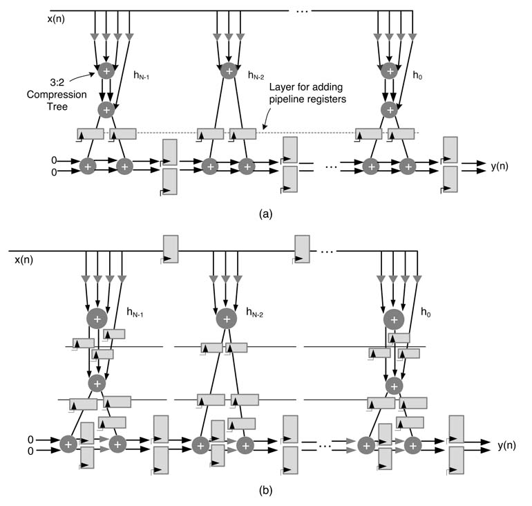
The chapter discusses mapping a signal processing algorithm represented as a dataflow graph (DFG) on optimal hardware. The optimization techniques extensively use compression trees and avoid the use of CPAs, because from the area and timing perspectives a fast CPA is one of the most expensive building blocks in FDA implementation. The DFG can be transformed to avoid or reduce the use of CPAs. The technique is applied on IIR systems as well. These systems are recursive in nature. All the multipliers are implemented as compression trees that reduce all PPs to two layers of carry and sum. These two layers are not added inside the feedback loop, rather they are fed back as a partial solution to the next block. This helps in improving the timing of the implementation.
6.2 Canonic Signed Digit Representation
CSD is a radix-2 signed-digit coding. It codes a constant using signed digits 1, 0 and — 1 [1, 2]. An N-bit constant C is represented as:
The expression implies that the constant is coded using signed digits 1,0 or — 1, where each digit si contributes a weight of 2 i to the constant value. The CSD representation has the following properties:
- No two consecutive bits in CSD representation of a number are non-zero.
- The CSD representation of a number uses a minimum number of non-zero digits.
- The CSD representation of a number is unique.
CSD representation of a number can be recursively computed using the string property. The number is observed to contain any string of 1s while moving from the least significant bit (LSB) to the most significant (MSB). The LSB in a string of 1s is changed to 1 that represents — 1, and all the other 1s in the string are replaced with zeros, and the 0 that marks the end of the string is changed to 1. After replacing a string by its equivalent CSD digits, the number is observed again moving from the coded digit to the MSB to contain any further string of 1s. The newly found string is again replaced by its equivalent CSD representation. The process is repeated until no string of 1s is found in the number.
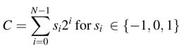
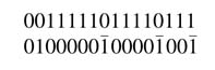
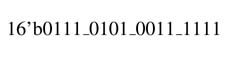
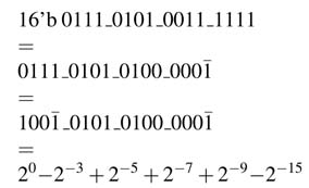
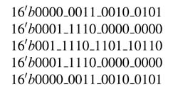
Example: Converting 16'b0011_1110_1111_0111 to CSD representation involves the following recursion. Find a string while moving from LSB to MSB and replace it with its equivalent CSD representation:
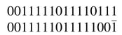
The newly formed number is observed again for any more string of 1s to be replaced by its equivalent CSD representation:
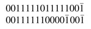
The process is repeated until all strings of 1s are replaced by their equivalent CSD representations:
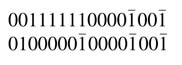
All these steps can be done simultaneously by observing isolated strings or a set of connected strings with one 0 in between. All the isolated strings with more than one 0 in between are replaced by their equivalent CSD representations, and for each connected string all the 0s connecting individual strings are changed to 1, and all the 1s in the strings are all changed to 0. The equivalent CSD representation computed in one step is:
6.3 Minimum Signed Digit Representation
MSD drops the condition of the CSD that does not permit two consecutive non-zero digits in the representation. MSD adds flexibility in representing numbers and is very useful in HW implementation of signal processing algorithms dealing with multiplication with constants. In CSD representation a number is unique, but a number can have more than one MSD representation with minimum number of non-zero digits. This representation is used in later in the chapter for optimizing the HW design of algorithms that require multiplication with constant numbers.
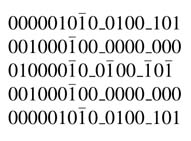
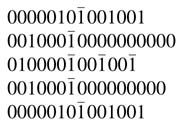
Example: The number 51 (=7'b0110011) has four non-zero digits, and the number is CSD representation, 1010101, also has four non-zero digits. The number can be further represented in the following MSD format with four non-zero digits:

6.4 Multiplication by a Constant in a Signal Processing Algorithm
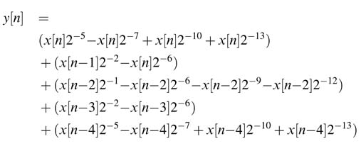
As stated earlier, in many DSP and digital communication algorithms a large proportion of multiplications are by constants. For FDA the complexity of a general-purpose multiplier is not required as PPs for only non-zero bits of the multiplier are generated. For example, when implementing the difference equation given by:
y[n — 1] is multiplied by 0.916. In Q1.15 format the number is:
As 11 bits in the constant are non-zero, PPs for these bits should be generated, whereas a general-purpose multiplier requires the generation of 16PPs. Representing the constant in CSD form further reduces the number of PPs.
Here the constant in the equation is transformed to CSD representation by recursively applying the string property on the binary representation of the number:
The CSD representation of the constant thus reduces the number of non-zero digits from 11 to 6. For multiplication of 0.916 with y[n — 1] in FDA implementation thus requires generating only 6PPs. These PPs are generated by appropriately shifting y[n — 1] by weight of the bits in Q1.15 format representation of the constant as CSD digits. The PPs are:
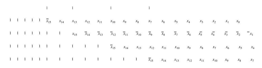
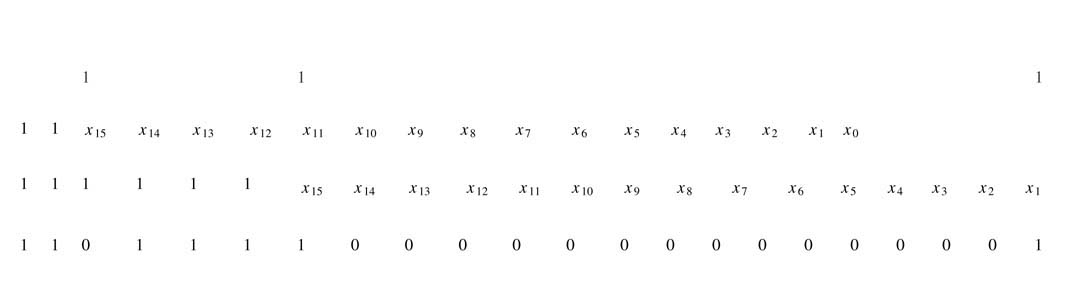
The PPs are generated by hardwired right shifting of y[n — 1] by 0,3,5,7,9 and 15 and adding or subtracting these PPs according to the sign of CSD digits at these locations. The architecture can be further optimized by incorporating x[n] as the seventh PP and adding CV for sign extension elimination logic as the eighth PP in the compression tree. All these inputs to the compression tree are mathematically shown here:
The CV is calculated by adding the correction for multiplication by 1 and 1 in the CSD representation of the number. The CV calculation follows the method given in Chapter 5. For multiplication by 1 the CV is computed by flipping the sign bit of the PP and adding 1 at the location of the sign bit and then extending the number by all 1s. Whereas for multiplication by 1 the PP is generated by taking the one’s complement of the number. This sign extension and two’s complement in this case require flipping of all the bits of the PP except the sign bit, adding 1 at the locations of the sign bit and the LSB, and then extending the number by all 1s. Adding contribution of all the 1s from all PPs gives us the CV:
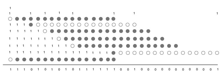
Figure 6.1 shows the CV calculation. The filled dots show the original bits and empty dots show flipped bits of the PPs. Now these eight PPs can be reduced to two layers of partial sums and carries using any compression method described in Chapter 5.
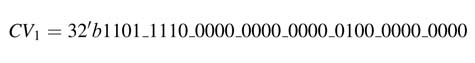
Figure 6.2 shows the use of Wallace tree in reducing the PPs to two. Finally these two layers are added using any fast CPA. The compression is shown by all bits as filled dots.
6.5 Optimized DFG Transformation
Several architectural optimization techniques like carry save adder (CSA), compression trees and CSD multipliers can be used to optimize DFG for FDA mapping. From the area and timing
Figure 6.1 CV calculation
perspectives, a CPA is one of the most expensive building blocks in HW implementation. In FDA implementation, simple transformations are applied to minimize the use of CPAs.
Figure 6.3(a) shows the DFG mapping of (6.1). If implemented as it is, the critical path of the design consists of one multiplier and one adder. Section 6.4 showed the design for FDA by using a compression tree that reduces all the PPs consisting of terms for CSD multiplication, x[n] and CV for sign extension elimination. The design then uses a CPA and reduces the two layers from the
Figure 6.2 Use of the Wallace tree for PP reduction to two layers
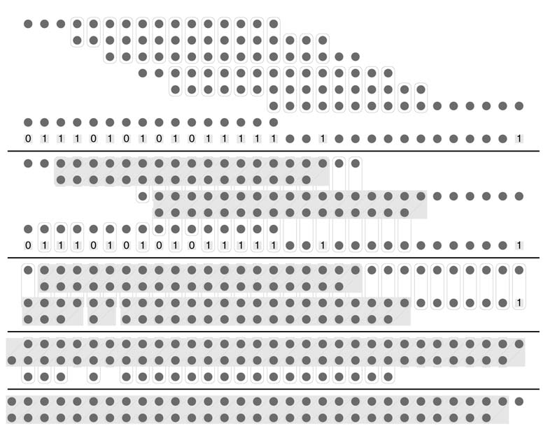
Figure 6.3 First-order IIR filter. (a) DFG with one adder and one multiplier in the critical path. (b) Transformed DFG with Wallace compression tree and CPA outside the feedback loop
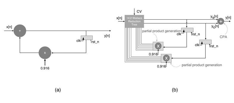
reduction tree to compute y[n] . In instances where further improvement in the timing is required, this design needs modification.
It is important to note that there is no trivial way of adding pipeline registers in a feedback loop as it changes the order of the difference equation. There are complex transformations, which can be used to add pipeline registers in the design[3–5].The timing can also be improved without adding any pipeline registers. This is achieved by taking the CPA out of the feedback loop, and feeding in the loop y s [n] and y c [n] that represent the partial sum and partial carry of y[n] . Once the CPA is outside the loop, it can be pipelined to any degree without affecting the order of the difference equation it implements.
The original DFG is transformed into an optimized DFG as shown in Figure 6.3(b). As the partially computed results are fed back, this requires duplication of multiplication and storage logic and modification in (6.1) as:
Although this modification increases the area of the design, it improves the timing by reducing the critical path to a compression tree as the CPA is moved outside the feedback loop.
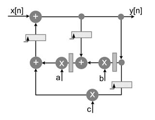
Example: Figure 6.4(a) shows a Direct Form (DF)-II implementation of a second-order IIR filter [6]. The difference equation of the filter is:
For HW implementation of the design, all the coefficients are converted to fixed-point and then translated to CSD representation. Without loss of generality, we may consider four non-zero bits in CSD representation of each coefficient. For this, each multiplier is implemented using four PPs. Moving the CPAs to outside the filter structure results in elimination of all CPAs from the filter. As the sums and carries are not added to get the sum, the results flow in partial computed form in the datapath. These partial results double the PP generation logic and registers in the design, as shown in Figures 6.4(b)and(c).Each pair of CSD multipliers now generates PPs for the partial sum, and as well as partial carries These PPs are compressed in two different settings of the compression trees. These two set of PPs and their compression using a Wallace reduction tree are shown in Figures 6.4(b)and(c).
Another design option is to place CPAs in the feedforward paths and pipelining them if so desired. This option is shown in Figure 6.4(d). For each pair of multipliers a CV is calculated, which takes
Figure 6.4 Second-order IIR filter. (a) DF-II dataflow graph. (b) Optimized implementation with CSD multipliers, compression trees and CPA outside the IIR filter. (c) Using unified reduction trees for the feedforward and feedback computations and CPA outside the filter. (d) CPA outside the feedback loop only
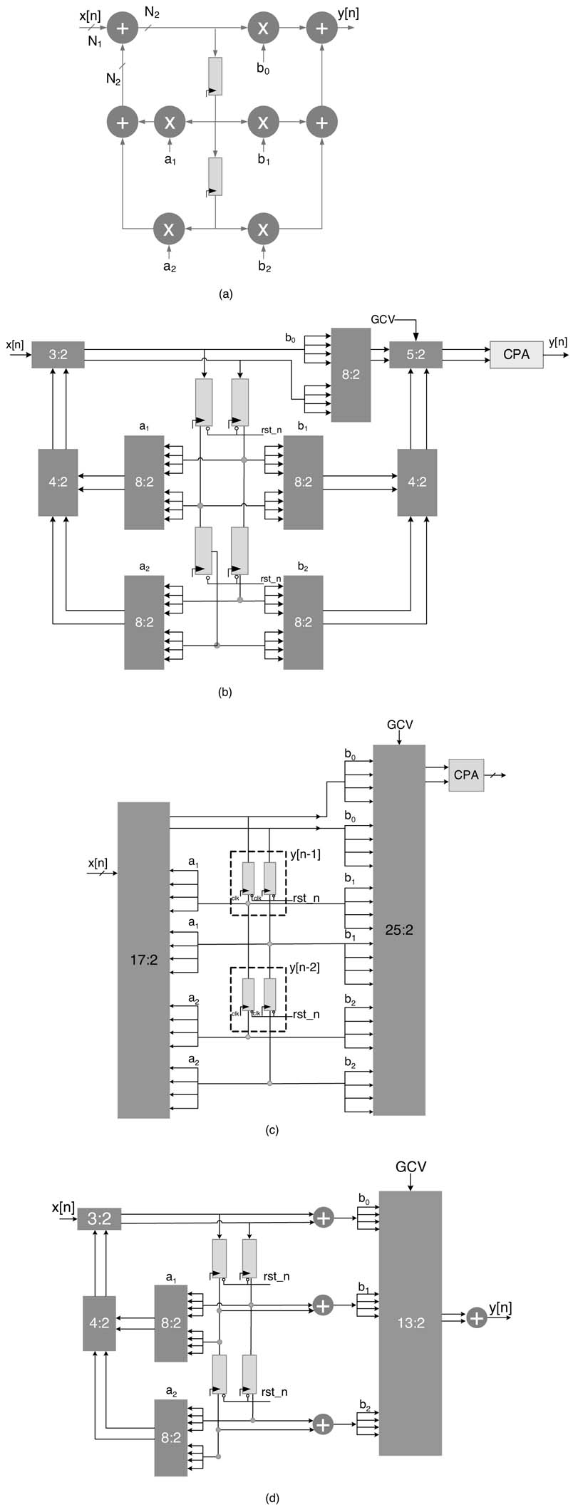
care of sign-extension elimination and two’s complement logic. A global CV (GCV)is computed by adding all the CVs. The GCV can be added in any one of the compression trees. The figure shows the GCV added in the compression tree that computes final sum and carry, y s [n] and y c [n]. A CPA is placed outside the loop. The adder adds the partial results to generate the final output. Once the CPA is outside the loops, it can be pipelined to any degree without affecting the order of the difference equation it implements.
If there are more stages of algorithm in the application, to get better timing performance the designer may chose to pass the partial results without adding them to the next stages of the design.
6.6 Fully Dedicated Architecture for Direct-form FIR Filter
6.6.1 Introduction
The FIR filter is very common in signal processing applications. For example it is used in the digital front end (DFE) of a communication receiver. It is also used in noise cancellation and unwanted frequency removal from received signals in a noisy environment. In many applications, the signal may be sampled at a very high rate and the samples are processed by an FIR filter. The application requires an FDA implementation of a filter executing at the sampling clock.
The FIR filter is implemented using the convolution summation given by:
(6.4)
where the h[k] represent coefficients of the FIR filter, and x[n] represents the current input sample and x[n — k] is the k th previous sample. For simplicity this chapter sometimes writes indices as subscripts:
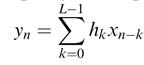
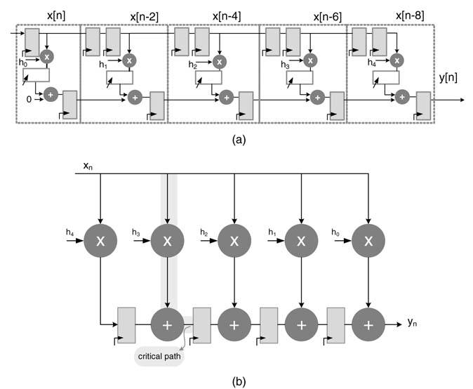
A block diagram of an FIR filter for L = 5 is shown in Figure 6.5(a). This structure of the FIR filter is known as direct-form (DF) [6]. There are several other ways of implementing FIR filters, as discussed later.
In a DF implementation, to compute output sample y n , the current input sample x n is multiplied with h 0 , and for each k each previous x n-k sample is multiplied by its corresponding coefficient h k and finally all the products are added to get the final output. An FDA implementation requires all these multiplications and additions to execute simultaneously, requiring L multipliers and L — 1 adders. The multiplication with constant coefficients can exploit the simplicity of the CSD multiplier [7].
Each of these multipliers, in many design instances, is further simplified by restricting the number of non-zero CSD digits in each coefficient to four. One non-zero CSD digit in a coefficient approximately contributes 20 dB of stop-band attenuation [8], so the four most significant non-zero CSD digits in each coefficient attains around 80 dB of stop-band attenuation. The stop band attenuation is a measure of effectiveness of a filter and it represents how successfully the filter can stop unwanted signals.
Figure 6.5(b) shows each CSD multiplier with four non-zero digits generating four PPs. One approach is to compute the products by accumulating four PPs for each multiplication and then sum these products to get the final answer. A better approach is to reduce all the PPs generated for all multiplications and the GCV to two layers using a Wallace or Dadda reduction scheme. The two layers then can be summed using any fast CPA. The GCV is computed by adding CVs for each multiplication. Figure 6.5(b) shows the optimized architecture for a 5-coefficient FIR filter. More optimized solutions for FIR architectures are proposed in the literature. These solutions work on complexity reduction and are discussed in a later section.
Figure 6.5 Five-coefficient FIR filter. (a) DF structure. (b) All multiplications are implemented as one compression tree and a single CPA
6.6.2 Example: Five-coefficient Filter
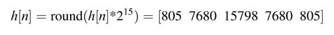
Consider the design of a 5-coefficient FIR filter with cutoff frequency π/4 . The filter is designed using the fir1() function in MATLAB ® . Convert h[n] to Q1.15 format. Compute the CSD representation of each fixed-point coefficient. Design an optimal DF FDA architecture by keeping a maximum of four most significant non-zero digits in the CSD representation of the filter coefficients. Generate all PPs and also incorporate CV in the reduction tree. Use the Wallace reduction technique to reduce the PPs to two layers for addition using any fast CPA.
Solution: The five coefficients of the filter in double-precision floating-point using the MATLAB ® fir1 function are:
Converting h[n] into Q1.15 format gives:
Binary representation of the coefficients is:
Converting the coefficients into CSD representation gives:
Keeping a maximum of four non-zero CSDs in each coefficient results in:
The sixteen PPs are as follows:
For sing-extension elimination, five CVs for each multiplier are computed and added to form the GCV. The computed CV 0 for the first coefficient is shown in Figure 6.6, and so:
Figure 6.6 Computation for CV 0 (see text)
The computed CV 1 for the second coefficient is shown in Figure 6.7, and so:
Following the same procedure, the CV 2 computes to:
Because of symmetry of the coefficients, CV 3 and CV 4 are the same as CV 1 and CV 0 , respectively. All these correction vectors are added to get the GCV:
This correction vector is added for sign-extension elimination.
The implementation of three designs in RTL Verilog is given in this section. The moduleFIRfilter uses multipliers and adders to implement the FIR filter, whereas module FIRfilterCSD converts the filter coefficients in CSD format while considering a maximum of four non-zero CSD digits for each coefficient. There are a total of 16PPs that are generated and added to show the equivalence of the design with the original format. The code simply adds the PP whereas, in actual designs, the PPs should be compressed using Wallace or Dadda reduction schemes. Finally, the module FIRfilterCV implements sign-extension elimination logic by computing a GCV. The vector is added in place of all the sign bits and 1s that are there to cater for two’s complement in the PPs. The Verilog code of the three modules with stimulus is listed here.
// Module uses multipliers to implement an FIR filter
module FIRfilter
input signed [15:0] x,
input clk,
output reg signed [31:0] yn);
reg signed [15:0] xn [0:4];
wire signed [31:0] yn_v;
// Coefficients of the filter wire signed [15:0] h0 = 16’h0325; wire signed [15:0] h1 = 16’h1e00; wire signed [15:0] h2 = 16’h3DB6; wire signed [15:0] h3 = 16’h1e00; wire signed [15:0] h4 = 16’h0325;
// Implementing filters using multiplication and addition operators assign yn_v = (h0*xn[0] + h1*xn[1] + h2*xn[2] + h3*xn[3] + h4*xn[4]); always @(posedge clk)
begin
 // Tap delay line of the filter
 xn[0] <= x;
 xn[1] <= xn[0];
Figure 6.7 Computation for CV1 (see text)
xn[2] <= xn[1];
xn[3] <= xn[2];
xn[4]<= xn[3];
// Registering the output
yn <= yn_v; end
endmodule
// Module uses CSD coefficients for implementing the FIR filter module FIRfilterCSD (input signed [15:0] x, input clk,
output reg signed [31:0] yncsd); reg signed [31:0] yncsd_v; reg signed [31:0] xn [0:4]; reg signed [31:0] pp[0:15];
always @(posedge clk)
begin
// Tap delay line of FIR filter
xn[0] <= {x, 16’h0};
xn[1] <= xn[0];
xn[2] <= xn[1];
xn[3] <= xn[2];
xn[4]<= xn[3];
yncsd <= yncsd_v; // registering the output
end
always @ (*)
begin
// Generating PPs using CSD representation of coefficients
// PP using 4 significant digits in CSD value of coefficient h 0
pp[0] = xn[0]>>>5;
pp[1] = -xn[0]>>>7;
pp[2] = xn[0]>>>10;
pp[3] = xn[0]>>>13;
// PP using CSD value of coefficient h 1
pp[4] = xn[1]>>>2;
pp[5] = - xn[1]>>>6;
// PP using 4 significant digits in CSD value of coefficient h 2
pp[6] = xn[2]>>>1;
pp[7] = -xn[2]>>>6;
pp[8] = -xn[2]>>>9;
pp[9] = -xn[2]>>>12;
// PP using CSD value of coefficient h 3
pp[10] = xn[3]>>>2;
pp[11] = -xn[3]>>>6;
// PP using 4 significant digits in CSD value of coefficient h 4
pp[12] = xn[4]>>>5;
pp[13] = -xn[4]>>>7;
pp[14] = xn[4]>>>10;
pp[15] = xn[4]>>> 13;
// Adding all the PPs, the design to be implemented in a 16:2 compressor
yncsd_v = pp[0]+pp[1]+pp[2]+pp[3]+pp[4]+pp[5]+
pp[6]+pp[7]+pp[8]+pp[9]+pp[10]+pp[11]+
pp[12]+pp[13]+pp[14]+pp[15];
end
endmodule
// Module uses a global correction vector by eliminating sign extension logic
module FIRfilterCV (
input signed [15:0] x,
input clk,
output reg signed [31:0] yn
);
reg signed [31:0] yn_v;
regsigned [15:0] xn_0, xn_1, xn_2, xn_3, xn_4;
reg signed [31:0] pp[0:15];
// The GCV is computed for sign extension elimination
reg signed [31:0] gcv = 32’
b0110_1111_0111_0000_0001_0000_1001_0000;
always @(posedge clk)
begin
// Tap delay line of FIR filter
xn_0 <= x;
xn_1 <= xn_0;
xn_2 <= xn_1;
xn_3 <= xn_2;
xn_4 <= xn_3;
yn <= yn_v; // registering the output
end
always @ (*)
begin
// Generating PPs for 5 coefficients
// PPs for coefficient h 0 with sign extension elimination
pp[0]= {5’b0, ~xn_0[15], xn_0[14:0], 11’b0};
pp[1] = {7’b0, xn_0[15], ~xn_0[14:0], 9’b0};
pp[2] = {10’b0, ~xn_0[15], xn_0[14:0],6’b0};
pp[3] = {13’b0, ~xn_0[15], xn_0[14:0],3’b0};
// PPs for coefficient h1 with sign extension elimination
pp[4] = {2’b0, ~xn_1[15], xn_1[14:0], 14’b0};
pp[5] = {6’b0, xn_1[15], ~xn_1[14:0], 10’b0};
// PPs for coefficient h 2 with sign extension elimination
pp[6] = {1’b0, ~xn_2[15], xn_2[14:0], 15’b0};
pp[7] = {6’b0, xn_2[15], ~xn_2[14:0], 10’b0};
pp[8] = {9’b0, xn_2[15], ~xn_2[14:0], 7’b0};
pp[9] = {12’b0, xn_2[15], ~xn_2[14:0], 4’b0};
// PPs for coefficient h 3 with sign extension elimination
pp[10] = {2’b0, ~xn_3[15], xn_3[14:0], 14’b0};
pp[11] = {6’b0, xn_3[15], ~xn_3[14:0], 10’b0};
// PPs for coefficient h 4 with sign extension elimination
pp[12]= {5’b0, ~xn_4[15], xn_4[14:0], 11’b0};
pp[13] = {7’b0, xn_4[15], ~xn_4[14:0], 9’b0};
pp[14] = {10’b0, ~xn_4[15], xn_4[14:0],6’b0};
pp[15] = {13’b0, ~xn_4[15], xn_4[14:0],3’b0};
// Adding all the PPs with GCV
// The design to be implemented as Wallace or Dadda reduction scheme
yn_v = pp[0]+pp[1]+pp[2]+pp[3]+
pp[4]+pp[5]+
pp[6]+pp[7]+pp[8]+pp[9]+
pp[10]+pp[11]+
pp[12]+pp[13]+pp[14]+pp[15]+gcv;
end
endmodule
module stimulusFIRfilter;
reg signed [15:0] X;
reg CLK;
wire signed [31:0] YN, YNCV, YNCSD;
integer i;
// Instantiating all the three modules for equivalency checking
FIRfilterCV FIR_CV(X, CLK, YNCV);
FIRfilterCSD FIR_CSD(X, CLK, YNCSD);
FIRfilter FIR(X, CLK, YN);
initial
begin
CLK = 0;
X = 1;
#1000 $finish;
end
// Generating clock signal
always
#5 CLK = ~CLK; // Generating a number of input samples initial
begin
for (i=0; i<256; i=i+1)
#10 X = X+113;
end
initial
$monitor ($time, " X=%h, YN=%h, YNCSD=%h, YNCV=%h
", X, YN<<1, YNCSD, YNCV);
endmodule
6.6.3 Transposed Direct-form FIR Filter
The direct-form FIR filter structure of Figure 5.5 results in a large combinational cloud of reduction tree and CPA. The cloud can be pipelined to reduce the critical path delay of the design.
Figure 6.8(a) shows a 5-coefficient FIR filter, pipelined to reduce the critical path delay of the design. Now the critical path consists of a multiplier and an adder. Pipelining causes latency and a large area overhead in implementing registers. This pipeline FIR filter can be best mapped on the Vertix™-4 and Vertix™-5 families of FPGAs with embedded DSP48 blocks. The effectiveness of this mapping is demonstrated in Chapter 5.
In many design instances, using general-purpose multipliers of DSP48 blocks may not be appropriate as they are a finite resource and should be used for parts of the algorithm that require
Figure 6.8 (a) Pipeline direct-form FIR filter best suited for implementation on FPGAs with DSP48-like building blocks. (b) TDF structure for optimal mapping of multipliers as CSD shift and add operation
multiplication by non-constant values. For many applications requiring multiplication by constants, CSD multiplication usually is the most optimal option.
Retiming is an effective technique to systematically move algorithmic delays in a design to reduce the critical path of the logic circuit. In Chapter 7, retiming is applied to transform the filter given in Figure 6.8(a) to get an equivalent filter shown in Figure 6.8(b). This new filter is the transposed direct form [6]. It is interesting to observe that in this form, without adding pipelining registers, the algorithm delays are systematically moved using retiming transformation from the upper edge of the DFG to the lower edge. This has resulted in reducing the critical path of an L-coefficient FIR filter from one multiplier and L — 1 adders of direct form to one multiplier and an adder as shown in Figure 6.8(b).
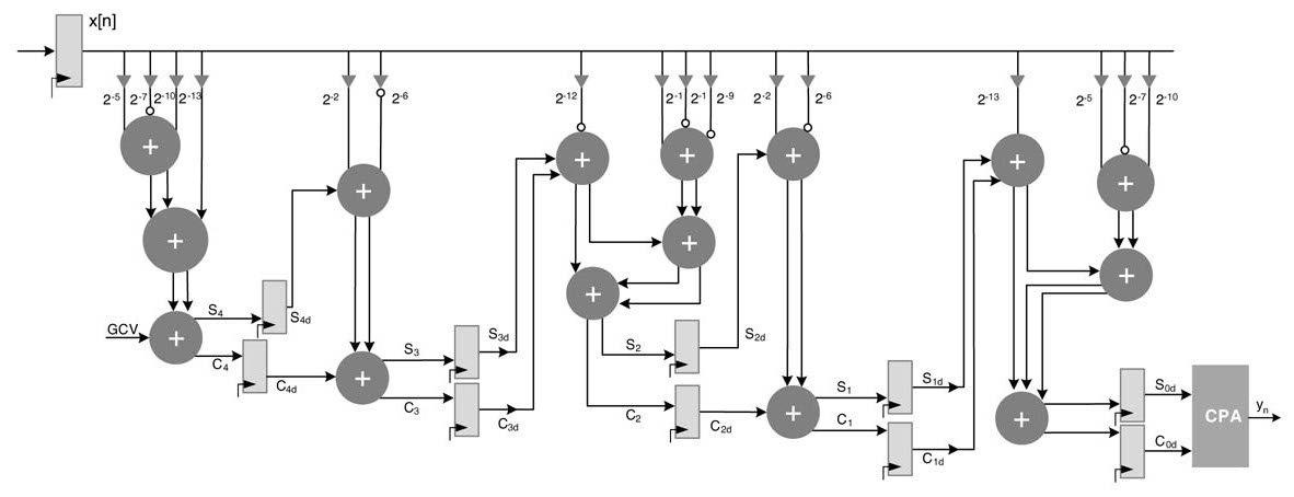
In FDA designs of a TDF FIR filter, each constant in the multiplier is converted to CSD representation and then appropriate PPs are generated for non-zero digits in CSD representation of the coefficients. These PPs are reduced by carry save reduction to two layers. The outputs of these two layers are respectively stored in two registers. Although this doubles the number of registers in the design, it removes CPAs which otherwise are required to add the final two layers into one for each coefficient multiplication. Figure 6.9 shows the TDF FIR filter implemented as CSD multiplication and carry save addition. Each multiplier represents the generation of PPs for non-zero digits in CSD representation of the coefficients and their reduction to two layers using the carry save reduction scheme.
The critical path can be further reduced by adding pipeline layers in the design, as shown in Figure 6.10(a). Inserting appropriate levels of pipelining can reduce the critical path to just
Figure 6.9 Transposed direct-form FIR filter with CSD multiplication and carry save addition

Figure 6.10 (a) TDF FIR filter with one stage of pipelining registers. (b) Deeply pipelined TDF FIR filter with critical path equal to one full adder delay
a fuller-adder delay. This critical path is independent of filter length. A deeply pipelined filter with one FA in the critical path is shown in Figure 6.10(b). A pipeline register is added after every carry save adder. To maintain the data coherency in the pipeline architecture, registers are added in all parallel paths of the architecture. Although a designer can easily place these registers by ensuring that the coherent data is fed to each computational node in the design, a cut-set transformation provides convenience in finding the location of all pipeline registers. This is covered in Chapter 7.
6.6.4 Example: TDF Architecture
Consider the design of a TDF architecture for the filter in Section 6.6.2.
Solution: A maximum of four non-zero digits in CSD representation of each coefficient are given here:
For TDF we need to produce the following PPs for each multiplier M k :
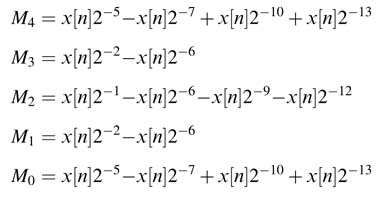
Each PP is generating by hardwired shifting of x[n] by the respective non-zero CSD digit. These PPs for each coefficient multiplication are reduced to two layers using a carry save adder. The result from this reduction {c k , s k } is saved in registers {c kd , s kd }:
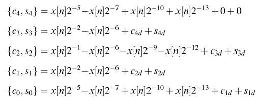
The values in c 0 and s 0 are either finally added using any CPA to compute the final result, or they are forwarded in the partial formtothe next stage of the algorithm. The CPAis notin the critical path and can be deeply pipelined as desired.
An RTL design of the filter is shown in Figure 6.11 and the corresponding Verilog code is given here.
Figure 6.11 RTL design of the 5-coefficient TDF filter of the text example
// Module using TDF structure and 3:2 compressors
module FIRfilterTDFComp (
input signed [15:0] x,
input clk,
output signed [31:0] yn);
integer i;
reg signed [15:0] xn;
//Registersforpartialsums,asfilterissymmetric,thecoefficientsarenumbered
// for 0, 1, 2,…, 4 rather 4, 3,…, 0
reg signed [31:0] sn_0, sn_1, sn_2, sn_3, sn_4;
// Registers for partial carries
reg signed [32:0] cn_0, cn_1, cn_2, cn_3, cn_4;
reg signed [31:0] pp_0, pp_1, pp_2, pp_3, pp_4, pp_5,
pp_6, pp_7, pp_8, pp_9, pp_10, pp_11,
pp_12, pp_13, pp_14, pp_15; // Wires for compression tree for intermediate sums and carries reg signed [31:0] s00, s01, s10, s11, s20, s200, s21, s30,
s31, s40, s400, s41, s02, s22, s42; reg signed [32:0] c00, c01, c10, c11, c20, c200, c21, c30,
c31, c40, c400, c41, c02, c22, c42; // The GCV computed for sign extension elimination
reg signed [31:0] gcv = 32’b0110_1111_0111_0000_0001_0000_1001_0000;
// Add final partial sum and carry using CPA assign yn = cn_4+sn_4; always @(posedge clk)
begin
 xn <= x; // register the input sample
 // Register partial sums and carries in two sets of
 registers for every coeff multiplication
 cn_0 <= c02;
 sn_0 <= s02;
 cn_1 <= c11;
 sn_1 <= s11;
 cn_2 <= c22;
 sn_2 <= s22;
 cn_3 <= c31;
 sn_3 <= s31;
 cn_4 <= c42;
 sn_4 <= s42;
end
always @ (*)
begin
 // First level of 3:2 compressors, initialize 0 bit of all carries that are not used c00[0]=0; c10[0]=0; c20[0]=0; c200[0]=0; c30[0]=0; c40[0]=0; 400[0]=0;
 for (i=0; i<32; i=i+1)
begin
 // 3:2 compressor at level 0 for coefficient 0 {c00[i+1],s00[i]} = pp_0[i]+pp_1[i]+pp_2[i]; // 3:2 compressor at level 0 for coefficient 1 {c10[i+1],s10[i]} = pp_4[i]+pp_5[i]+sn_0[i];
 // 3:2 compressor at level 0 for coefficient 2 {c20[i+1],s20[i]} = pp_6[i]+pp_7[i]+pp_8[i]; {c200[i+1],s200[i]} = pp_9[i]+sn_1[i]+cn_1[i]; // 3: 2 compressor at level 0 for coefficient 3 {c30[i+1],s30[i]} = pp_10[i]+pp_11[i]+sn_2[i]; // 3: 2 compressor at level 0 for coefficient 4 c40[i+1],s40[i]} = pp_12[i]+pp_13[i]+pp_14[i]; {c400[i+1],s400[i]} = pp_15[i]+sn_3[i]+cn_3[i]; end
 c01[0]=0; c11[0]=0; c21[0]=0; c31[0]=0; c41[0]=0; // Second level of 3:2 compressors for (i=0; i<32; i=i+1) begin
 // For coefficient 0
 {c01[i+1],s01[i]} =c00[i]+s00[i]+pp_3[i]; // For coefficient 1: complete {c11[i+1],s11[i]} =c10[i]+s10[i]+cn_0[i]; // For coefficient 2
 {c21[i+1],s21[i]} =c20[i]+s20[i]+c200[i]; // For coefficient3: complete {c31[i+1],s31[i]} =c30[i]+s30[i]+cn_2[i]; // For coefficient 4
 {c41[i+1],s41[i]} =c40[i]+s40[i]+c400[i]; end // Third level of 3:2 compressors c02[0]=0; c22[0]=0; c42[0]=0; for (i=0; i<32; i=i+1) begin // Add global correction vector {c02[i+1],s02[i]} =c01[i]+s01[i]+gcv [i];
 // For coefficient 2: complete {c22[i+1],s22 [i]} = c21[i]+s21[i]+s200[i]; // For coefficient 4: complete {c42[i+1], s42 [i]}= c41[i]+s41 [i]+s400[i];
 end
end
always @ (*)
begin
 // Generating PPs for 5 coefficients
 // PPs for coefficient h0 with sign extension elimination
 pp_0 = {5b0, ~xn[15], xn[14:0], 11b0};
 pp_1 = {7b0, xn[15], ~xn[14:0], 9b0};
 pp_2 = {10b0, ~ xn[15], xn[14:0],6b0};
 pp_3 = {13b0, ~xn[15], xn[14:0],3b0};
 // PPs for coefficient h1 with sign extension elimination
 pp_4 = {2b0, ~xn[15], xn[14:0], 14b0};
 pp_5 = {6b0, xn[15], ~xn[14:0], 10b0};
 // PPs for coefficient h2 with sign extension elimination
 pp_6= {1b0, xn[15], xn[14:0], 15b0};
 pp_7 = {6b0, xn[15], ~xn[14:0], 10b0};
 pp_8 = {9b0, xn[15], ~xn[14:0], 7b0};
 pp_9 = {12b0, xn[15], ~ xn[14:0], 4b0};
 // PPs for coefficient h3 with sign extension elimination
 pp_10 = {2b0, ~xn[15], xn[14:0], 14b0};
 pp_11 = {6b0, xn[15], ~xn[14:0], 10b0};
 // PPs for coefficient h4 with sign extension elimination
 pp_12 = {5b0, ~xn[15], xn[14:0], 11b0};
 pp_13 = {7b0, xn[15], ~xn[14:0], 9b0};
 pp_14 = {10b0, ~xn[15], xn[14:0],6b0};
 pp_15= {13b0, ~xn[15], xn[14:0],3b0};
end
endmodule
6.6.5 Hybrid FIR Filter Structure
Earlier sections have elaborated on architecture for a direct and transposed form FIR filter. These architectures are shown in Figures 6.12(a),(b). Both the architectures have their respective
Figure 6.12 FIR filter structures. (a) Direct-form structure. (b) Transposed-form structure. (c) Hybrid. (d) Direct–transposed hybrid
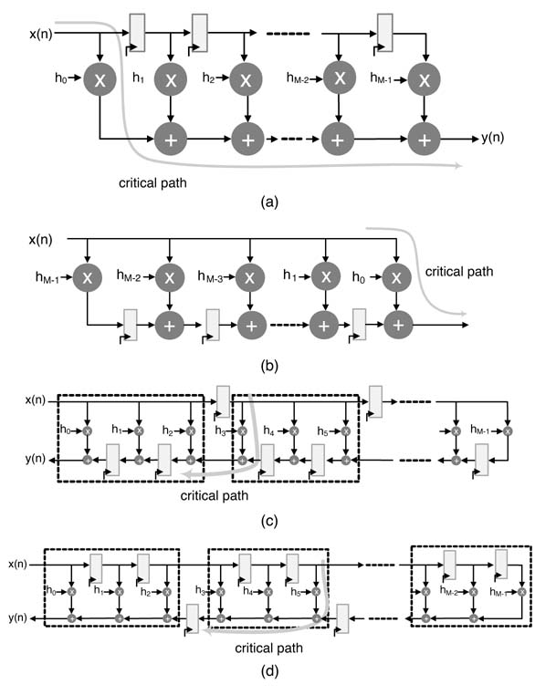
benefits and tradeoffs in HW mapping. The direct form requires only one set of registers and a unified compression tree to optimize the implementation and provide area-efficient designs, whereas the transposed form works on individual multiplications and keeps the results of these multiplications in sum and carry forms that require two sets of registers for holding the intermediate results. This form offers time-efficient designs. A mix of the two forms can also be used for achieving the best time–area tradeoffs. These forms are shown in Figures 6.12 (c) and (d).
6.7 Complexity Reduction
The TDF structure of an FIR filter implements multiplication of all coefficients with x[n], as shown in Figure 6.12(b). These multiplications can be implemented as one unit in a block. This consideration of one unit helps in devising techniques to further simplify the hardware of the block. All the multiplications in the block are searched to share common sub-expressions. This simplification targets reducing either the number of adders or the number of adder levels. The two approaches used for the HW reduction are sub-graph sharing and common sub-expression elimination [9].
6.7.1 Sub-graph Sharing
The algorithms that can be represented as a dependency graph can be optimized by searching constituent sub-graphs that are shared in the original graph. An algorithm that involves multiplication by constants of the same variable has great potential of sub-graph sharing. The sub-graphs, in these algorithms, are formed by generating all possible MSD (minimum signed digit) factors of each multiplication. An optimization algorithm minimizes the number of adders by selecting those options of the sub-graphs that are maximally shared among multiplications. The problem of generating all possible graphs and finding the ones that minimize the number of adders is a non-deterministic polynomial-time (NP)-complete problem. Many researchers have presented heuristic solutions for finding near optimal solutions of this optimization problem. A detailed description of these solutions is outside the scope of this book, so interested readers will find the references listed in this section very relevant. An n-dimension reduced adder graph (n-RAG) can be sub-optimally computed using efficient heuristics. Such a heuristic is listed in [10].
Example: This example is derived from [11]. An optimal algorithm in the graphical technique first generates multiple options of adder graphs for each multiplication. The algorithm then selects the graph out of all options for each multiplication that shares maximum nodes among all the graphs implementing multiplications by coefficients.
Consider a 3-coefficient FIR filter with the following 12-bit fixed-point values:
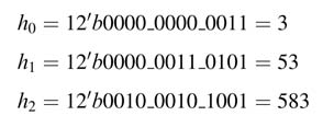
These coefficients are decomposed in multiple options. The decomposition is not unique and generates a search space. For the design in the example, some of the MSD decomposition options for each coefficient are:
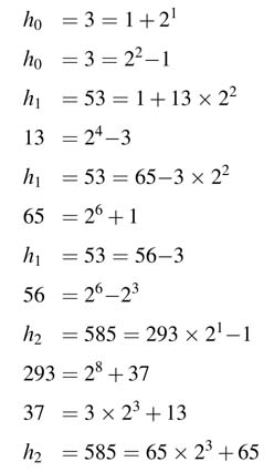
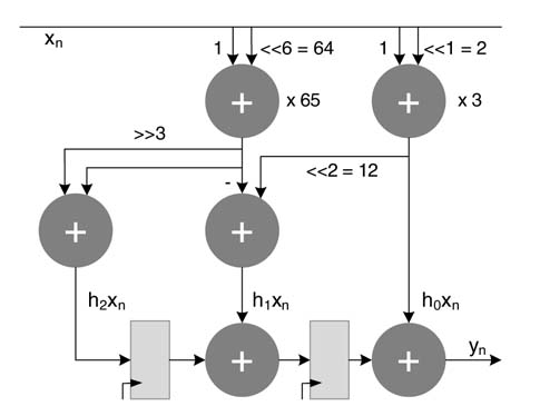
The graphical representations of these options are shown in Figure 6.13. Although there are several other options for each coefficient, only a few are shown to demonstrate that generating all these options and then finding the ones that maximize sharing of intermediate and final results is complex. For this example, the best solution picks the first sub-graph for h 0 and second sub-graphs for h 1 and h 2 . An optimized architecture that uses these options is shown in Figure 6.14.
Figure 6.13 Decomposition of {3,53,585} in sub-graphs for maximum sharing
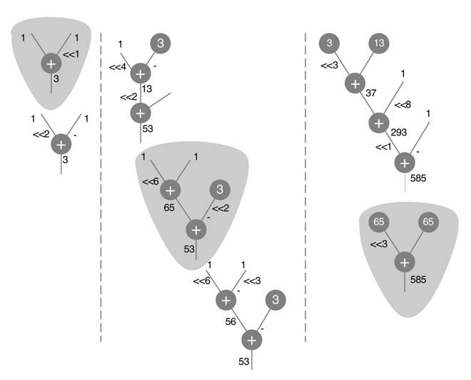
Figure 6.14 Selecting the optimal out of multiple decomposition options for optimized implementation of the FIR filter
6.7.2 Common Sub-expression Elimination
In contrast to graphical methods that decompose each coefficient into possible MSD factors and then find the factors for each multiplication that maximizes sharing, common sub-expression elimination (CSE) exploits the repetition of bits or digit patterns in binary, CSD or MSD representations of coefficients.
CSE works equally well for binary representation of coefficients, but to reduce the hardware cost the coefficients are first converted to CSD or MSD and are then searched for the common expressions. The technique is explained with the help of a simple example.
Example: Consider a two-tap FIR filter with h 0 = 5’ b 01110 and h 1 = 5’ b 01011 in Q1.4 format. Implementing this filter using TDF structure requires calculation of two products, h 0 x n and h 1 x n . These multiplications independently require the following shift and add operations:
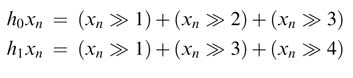
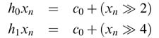
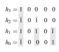
It is trivial to observe that two of the expressions in both the multiplications are common, and so needs to be computed once for computation of both the products. This reuse of common sub-expressions is shown here:
This value is then reused in both the expressions:
Several algorithms have been proposed in the literature to remove common sub-expressions [12, 13]. All these algorithms search for direct or indirect commonality that helps in reducing the HW complexity. Someof these methods are elucidated below for CSD and binary representations of coefficients.
6.7.2.1 Horizontal Sub-expressions Elimination
This method first represents each coefficient as a binary, CSD or MSD number and searches for common bits or digits patterns that may appear in these representations [12]. The expression is computed only once and then it is appropriately shifted to be used in other products that contain the pattern.
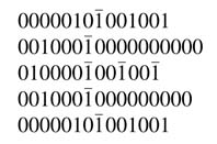
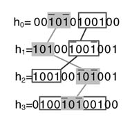
Example: For multiplication by constant 01_00111_00111, when converted to CSD format, gives 01.01001 -01001. The pattern 1001 appears twice in the representation. To optimize HW the pattern can be implemented only once and then the value is shifted to cater for the second appearance of the pattern, as shown in Figure 6.15.
Example: This example considers four coefficients. In Figure 6.16, the CSD representation of these constants reveals the digit patterns that can be shared. The common sub-expressions are shown as connected boxes. For the coefficient h 3 , there are two choices to select from. One option shares the 101 pattern, which has already been computed for h 0 , and the second option computes 1001 once and reuses it in the same expression to compute 1001.
6.7.2.2 Vertical Sub-expressions Elimination
This technique searches for bit or digit patterns in columns and those expression are computed once and reused across different multiplications [14]. The following example illustrates the methodology:
Here, ![]() apears four times. This expression can be computed once and then shared in the rest of the computation. To illustrate invertical bit locations methodology, the convolution summation is first written as:
apears four times. This expression can be computed once and then shared in the rest of the computation. To illustrate invertical bit locations methodology, the convolution summation is first written as:
Figure 6.15 To simplify hardware, sub-expression 01001 which is repeated twice in (a) is only computed once in (b)
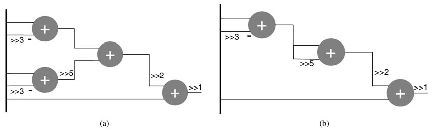
Figure 6.16 Common Sub-expressions for the example in the text
where x n z~ k represents x[n — k] for k = 0… 3. If the multiplications for the given coefficients are implemented as shift and add operations, then convolution summation of (6.6) can be written as:
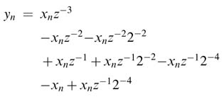
as z -1 represents a delay that makes x n z -1 = x n -1 , using it to extract common sub-expressions:
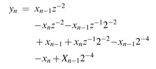
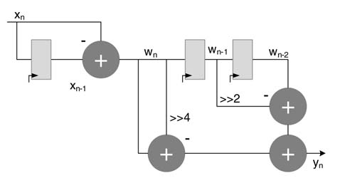
Let x n-1 -x n =w n . Then the convolution summation of (6.8) can be rewritten by using the common sub-expression of w n as:
The number of additions/subtractions is now reduced from eight to four. Figure 6.17 shows the optimized implementation.
Figure 6.17 Optimized implementation exploiting vertical common sub-expressions
6.7.2.3 Horizontal and Vertical Sub-expressions Elimination with Exhaustive Enumeration
This method searches for all possible enumerations of the bit or digit patterns with at least two nonzero bits in the horizontal and vertical expressions for possible HW reduction [13, 15].
For a coefficient with binary representation 010111, all possible enumerations witha minimum of two non-zero bits are as follows:
010100; 010010; 010001; 000110; 000101; 000011; 010110; 010101; 000111
Similarly, after writing all coefficients in binary representation, each of the columns is also enumerated with all patterns with more than one non-zero entries. Any of these expressions appearing in other columns can be computed once and used multiple times. Exhaustive enumeration, though, gives minimum hardware for the CSE problem but grows exponentially and becomes intractable for large filter lengths.
Example:
Combining the horizontal and vertical sharing of expressions, the convolution summation can be written as:
A common expression that shares vertical and horizontal sub-expressions can result in optimized logic. Let the expression be:
Then the convolution summation becomes:
The optimized architecture is shown in Figure 6.18.
Figure 6.18 Example of horizontal and vertical sub-expressions elimination
6.7.3 Common Sub-expressions with Multiple Operands
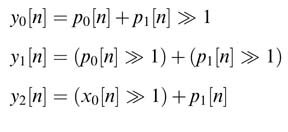
In many signal processing applications, the multiplication is with multiple operands, as in DCT,DFT or peak-to-average power ratio (PAPR) reduction using a precoding matrix in an orthogonal frequency-division multiplexed (OFDM) transmitter [16]. In these algorithms an extension of the method for common sub-expression elimination can also be used while computing more than one output sample as a linear combination of input samples [17]. Such a system requires computing matrix multiplication of the form:
This multiplication results in computing a linear combination of input sample for each output sample. The first equation is:
All the multiplications in the equation are implemented as multiply shift operations where the techniques discussed in this section for complexity reduction can be used for sub-graph sharing and common expression elimination. The example below highlights use of the common sub-expression elimination method on a set of equations for given constants.
Example:
In the following set of equations all the constants are represented in CSD format:
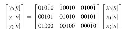
The required matrix multiplication using shift and add operations can be optimized by using the following sub-expressions:
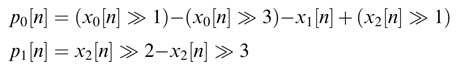
These sub-expressions simplify the computation of matrix multiplication as shown here:
6.8 Distributed Arithmetic
6.8.1 Basics
Distributed arithmetic (DA) is another way of implementing a dot product where one of the arrays has constant elements. The DA can be effectively used to implement FIR, IIR and FFT type algorithms [18–24]. For example, in the case of an FIR filter, the coefficients constitute an array of constants in some signed Q-format where the tapped delay line forms the array of variables which changes every sample clock. The DA logic replaces the MAC operation of convolution summation of (6.5) into a bit-serial look-up table read and addition operation [18]. Keeping in perspective the architecture of FPGAs, time/area effective designs can be implemented using DA techniques [19].
The DAlogic works byfirst expanding the array of variable numbers inthe dot product as a binary number and then rearranging MAC terms with respect to weights of the bits. A mathematical explanation of this rearrangement and grouping is given here.
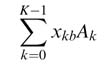
Let the different elements of arrays of constants and variables be A k and x k , respectively. The length of both the arrays is K . Then their dot product can be written as:
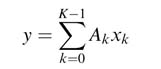
Without lost of generality, let us assume x k is an N-bit Q1. (N— 1)-format number:
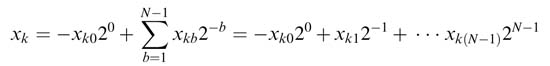
The dot product of (6.9) can be written as:
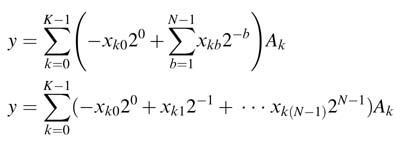
Rearranging the terms yields:
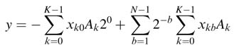
For K = 3 and N = 4, the rearrangement forms the following entries in the ROM:
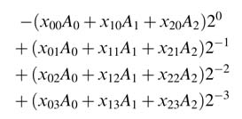
The DA technique pre-computes all possible values of
For the example under consideration, the summations for all eight possible values of x kb for a particular b and k = 0, 1 and 2 are computed and stored in ROM. The ROM is P bits wide and 2 K deep and implements a look-up table. The value of P is:
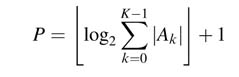
Table 6.1 ROM for distributed arithmetic
where ![]() is the floor operator that rounds a fraction value to its lower integer. The contents of the look-up table are given in Table 6.1.
is the floor operator that rounds a fraction value to its lower integer. The contents of the look-up table are given in Table 6.1.
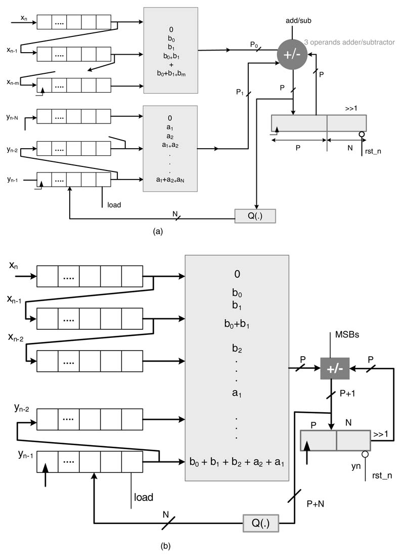
All the elements of the vector x =[ x 0 x1. … x K - 1 ] are stored in shift registers. The architecture considers in each cycle the bth bit of all the elements and concatenates them to form the address to the ROM. For the most significant bits (MSBs) the value in the ROM is subtracted from a running accumulator, and for the rest of the bit locations values from ROM are added in the accumulator. To cater for weights of different bit locations, in each cycle the accumulator is shifted to the right. To keep the space for the shift, the size of the accumulator is set to P + N, where a (P-bit adder adds the current output of the ROM in the accumulator and Nbits of the accumulator are kept to the right side to cater for the shift operation. The data is input to the shift registers from LSB. The dot product takes N cycles to compute the summation. The architecture implementing the dot product for K= 3, P = 5 and N = 4 is shown in Figure 6.19. FPGAs with look-up tables suit well DA-based filter design [20].
Example: Consider a ROM to compute the dot product of a 3-element vector with a vector of constants with the following elements :A 0 = 3,A1 = — 1 and A 2 = 5. Test the design for the following values in vector x:
Figure 6.19 DA for computing the dot product of integer numbers for N =4 and K¼3
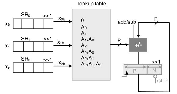
Table 6.2 Look-up table (LUT) for the text example
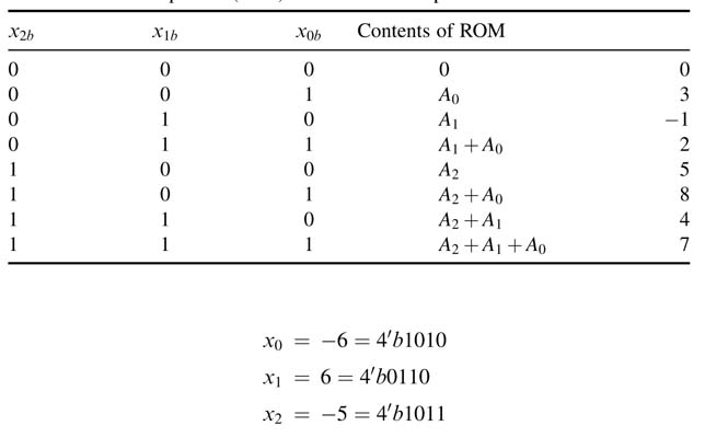
The contents of a 5-bit wide and 8-bit deep ROM are given in Table 6.2. The shift registers are assumed to contain elements of vector x with LSB in the right-most bit location.
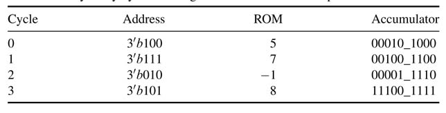
The cycle-by-cycle working of the DA architecture of Figure 6.20 for the case in consideration is given in Table 6.3. After four cycles the accumulator contains the value of the dot product: 9'M11001_111 = — 49 10 .
Figure 6.20 DA-based architecture for implementing an FIR filter of length L and N-bit data samples
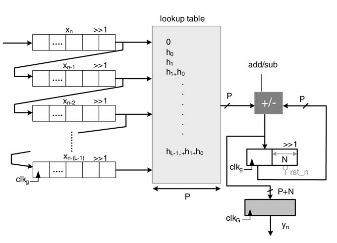
Table 6.3 Cycle by cycle working of DA for the text example
6.8.2 Example: FIR Filter Design
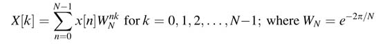
The DA architecture can be effectively used for implementing an FIR filter. The technique is of special interest in applications where the data is input to the system in bit-serial fashion. A DA-based design eliminates the use of a hardware multiplier and uses only a look-up table to provide high throughput execution at bit-rate irrespective of the filter length and width of the coefficients [21].
Figure 6.21 shows the architecture of an L-coefficient FIR filter. The data is input to the design in bit-serial fashion into shift register SR 0 , and all the shift registers are connected in a daisy-chain to form a tap delay line. The design works at bit clock clk g , and the design computes an output at every sample clk G , where sample clk G is N times slower than clk g .
RTL Verilog code of a DA-based 4-coefficient FIR filter is given below. The code also implements an FIR filter using convolution summation for equivalence checking:
/* Distributed arithmetic FIR filter
module FIRDistributedArithmetics
(
input xn_b, clk_g, rst_n,
input [3:0] contr,
output reg signed [31:0] yn,
output valid);
reg signed [31:0] acc; // accumulator
reg [15:0] xn_0, xn_1, xn_2, xn_3; // tap delay line
reg [16:0] rom_out;
reg [3:0] address;
wire signed [31:0] sum;
wire msb;
// DA ROM storing all the pre-computed values
always @(*)
begin
 //lsb of all registers
 address={xn_3[0],xn_2[0],xn_1[0],xn_0[0]};
 case(address)
 4’d0: rom_out=17’b00000000000000000;
 4’d1: rom_out=17’b00000001000100100; // h0
 4’d2: rom_out=17’b00011110111011100; // h1
 4’d3: rom_out=17’b00100000000000000; // h0+h1
 4’d4: rom_out=17’b00011110111011100; // h2
 4’d5: rom_out=17’b00100000000000000; // h2+h0
Figure 6.21 DA-based parallel implementation of an 18-coefficient FIR filter setting L= 3 and M= 6
 4’d6: rom_out=17’b00111101110111000; // h2+h1
 4’d7: rom_out=17’b00111110111011100; // h2+h1+h0
 4’d8: rom_out=17’b00000001000100100; // h3
 4’d9: rom_out=17’b00000010001001000; // h3+h0
 4’d10: rom_out=17’b00100000000000000; // h3+h1
 4’d11: rom_out=17’b00100001000100100; // h3+h1+h0
 4’d12: rom_out=17’b00100000000000000; // h3+h2
 4’d13: rom_out=17’b00100001000100100; // h3+h2+h0
 4’d14: rom_out=17’b00111110111011100; // h3+h2+h1
 4’d15: rom_out=17’b01000000000000000; // h3+h2+h1+h0
 default: rom_out= 17’bx;
 endcase
end
assign valid = ~ (|contr); // output data valid signal assign msb = contr // msb = 1 for contr = ff assign sum = (acc +
{rom_out^{17{msb}}, 16’b0} + // takes 1’s complement for msb
{15’b0, msb, 16’b0})> > >1; // add 1 at 16th bit location for 2’s complement logic
always @ (posedge clk_g or negedge rst_n)
begin
 if(!rst_n)
 begin
 // Initializing all the registers
 xn_0 <= 0;
 xn_1 <= 0;
 xn_2 <= 0;
 xn_3 <= 0; acc <= 0;
 end
else
 begin
 // Implementing daisy-chain for DA computation
 xn_0 <= {xn_b, xn_0[15:1]};
 xn_1 <= {xn_0[0], xn_1[15:1]};
 xn_2 <= {xn_1[0], xn_2[15:1]};
 xn_3 <= {xn_2[0], xn_3[15:1]};
 // A single adder should be used instead, shift right to multiply by 2-i
 if(&contr)
begin
yn <= sum;
acc <= 0;
end
 else
acc <= sum;
 end
end endmodule
// Module uses multipliers to implement an FIR filter for verification of DA arch
module FIRfilter
(
input signed [15:0] x,
input clk_s, rst_n,
output reg signed [31:0] yn);
reg signed [15:0] xn_0, xn_1, xn_2, xn_3;
wire signed [31:0] yn_v, y1, y2, y3, y4;
// Coefficients of the filter wire signed [15:0] h0 = 16’h0224; wire signed [15:0] h1 = 16’h3DDC; wire signed [15:0] h2 = 16’h3DDC; wire signed [15:0] h3 = 16’h0224;
// Implementing filters using multiplication and addition operators assign y1=h0*xn_0; assign y2=h1*xn_1; assign y3=h2*xn_2; assign y4=h3*xn_3;
assign yn_v = y1+y2+y3+y4;
always @(posedge clk_s or negedge rst_n)
begin
 if (!rst_n)
 begin
 xn_0<=0;
 xn_1<=0;
 xn_2<=0;
 xn_3<=0;
 end
else
 begin
 // Tap delay line of the filter
 xn_0 <= x;
 xn_1 <= xn_0;
 xn_2 <= xn_1;
 xn_3 <= xn_2;
 end
 // Registering the output
 yn <= yn_v;
end
endmodule
module testFIRfilter;
regsigned [15:0] X_reg, new_val;
reg CLKg, CLKs, RST_N;
reg [3:0] counter;
wire signed [31:0] YND;
wire signed [31:0] YN;
wire VALID, inbit;
integer i;
// Instantiating the two modules, FIRfilter is coded for equivalence checking
FIRDistributedArithmetics FIR_DA(X_reg[counter],
CLKg, RST_N, counter, YND, VALID);
FIRfilter FIR(new_val, CLKs, RST_N, YN);
initial
begin
 CLKg =0; // bit clock
 CLKs = 0; // sample clock
 counter = 0;
 RST_N = 0;
 #1 RST_N = 1;
 new_val=1;
 X_reg = 1;
 #10000 $finish;
end
// Generating clock signal always
 #2 CLKg = ~ CLKg; // fast clock always
 #32 CLKs = ~ CLKs; // 16 times slower clock
// Generating a number of input samples
always @ (counter)
begin
 // A new sample at every sample clock
 if (counter == 15) new_val = X_reg-1;
end
// Increment counter that controls the DA architecture to be placed in a controller
always @ (posedge CLKg)
begin
 counter <= counter+1;
 X_reg <= new_val; end initial
 $monitor ($time, " X_reg=%d, YN=%d, YND=%d
", X_reg, YN, YND); endmodule
It is obvious from the configuration of a DA-based design that the size of ROM increases with an increase in the number of coefficients of the filter. For example,a 128-coefficients FIR filter requires a ROM of size 2 128 . This size is prohibitively large and several techniques are used to reduce the ROM requirement [22–25].
6.8.3 M-parallel Sub-filter-based Design
This technique divides the filter into M sub-filters of length L , and each sub-filter is implemented as an independent DA-based module. For computing the output of the filter, the results of all M sub-filters are first compressed using any reduction tree, and the final sum and carry are added using a CPA. For a filter of length K , the length of each sub-filter is L =K/M . The filter is preferably designed to be of length LM , or one of the sub-filters may be of a little shorter length than the rest. For the parallel case, the convolution summation can be rewritten as:
The inner summation implements each individual sub-filter. These filters are designed using a DA-based MAC calculator. The outer summation then sums the outputs of all sub-filters. The summation is implemented as a compression tree and a CPA. The following example illustrates the design.
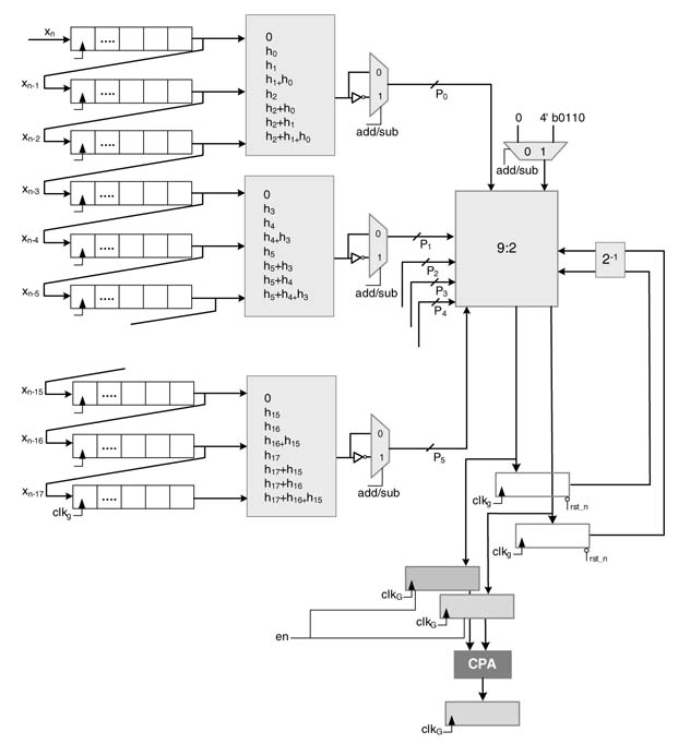
Example : The architecture designs an 18-coefficient FIR filter using six sub-filters. For the design L = 3 and M = 6, and the architecture is shown in Figure 6.21. Each sub-filter implements a 2 3 =8 deep ROM. The width of each ROM, P i for i = 0... 5, depends on the maximum absolute value of its contents. The output of each ROM is input to a compression tree. For the MSBs in the respective daisy-chain tap delay-line, the result needs to be subtracted. To implement this subtraction the architecture selects the one’s complement of the output from the ROM and a cumulative correction term for all the six sub-filters is added as 4’b0110 in the compression tree. The CPA is moved outside the accumulation module and the partial sum and partial carry from the compression tree is latched in the two sets of accumulator registers. The contents in the registers are also input to the compression tree. This makes the compression tree 9:2. If necessary the CPA adder needs to work on slower output sample-clock clk G , whereas the compression tree operates on fast bit-clock clk g . The final results from the compression trees are latched into two sets of registers clocked with clk G for final addition using a CPA and the two accumulator registers are reset to perform next set of computation.
6.8.4 DA Implementation without Look-up Tables
LUT-less DA implementation uses multiplexers. If the parallel implementation is extended to use M=K, then each shift register is connected to a two-entry LUT that either selects a 0 or the corresponding coefficient. The LUT can be implemented as a 2:1 MUX.
Designs for a 4-coefficient FIR filters are shown in Figure 6.22, using compression- and adder tree-based implementation. For the adder tree design the architecture can be pipelined at each adder stage if required.
The architectures of LUTand LUT-less implementation can be mixed to get a hybrid design. The resultant design has a mix of MUX- and LUT-based implementation. The design requires reduced sized LUTs.
Example : This example implements a DA-based biquadrature IIR filter. The transfer function of the filter is:
This transfer function translates into a difference equation given by:
The difference equation can be easily mapped on DA-based architecture. Either two ROMs can be designed for feed forward and feed back coefficients, or a unified ROM-based design can be realized. The two designs are shown in Figure 6.23. The value of the output, once computed, is loaded in parallel to a shift register for y[n — 1].
6.9 FFT Architecture using FIR Filter Structure
To fully exploit the potential optimization in mapping a DFT algorithm in hardware using techniques listed in this chapter, the DFT algorithm can be implemented as an FIR filter. This requires rewriting of the DFT expression as convolution summation. The Bluestein Chirp-z Transform (CZT) algorithm transforms the DFT computation problem into FIR filtering [25]. The CZT translates the nk term in the DFT summation in terms of (k — n ) for it to be written as a convolution summation.
Figure 6.22 A LUT-less implementation of a DA-based FIR filter. (a) A parallel implementation form = K uses a 2:1 MUX, compression tree and a CPA. (b) Reducing the output of the multiplexers using a CPA-based adder tree and one accumulator
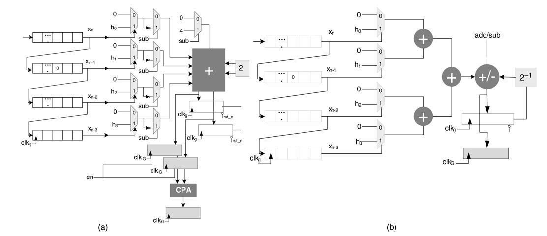
Figure 6.23 DA-based IIR filter design (a) Two ROM-based design. (b) One ROM-based design
The DFT summation is given as:
The nk term in (6.10) can be expressed as:
Substituting (6.10) in (6.11) produces the DFT summation as:
Using the circular convolution notation ⊗ , the expression in (6.12) can be written as:
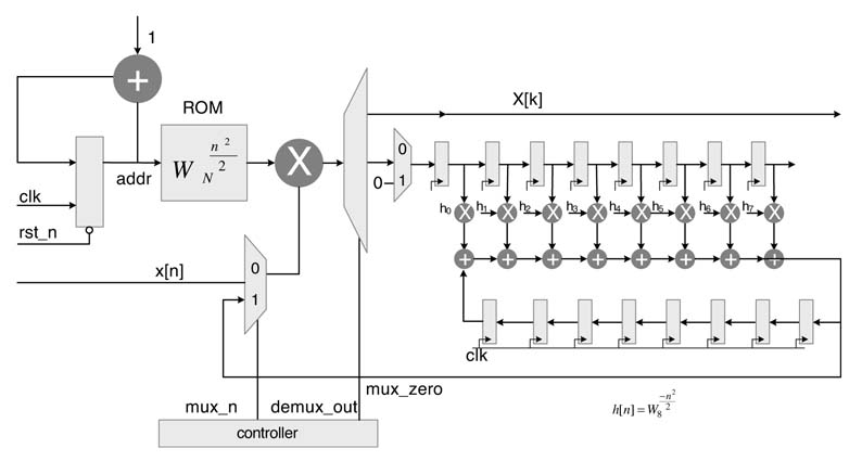
To compute an N-point DFT, the signal is first multiplied by an array of constants W N n 2 /2 . Then an N-point circular convolution is performed with an impulse response W N -n 2 . Finally the output of the convolution operation is again multiplied with an array of constants W N k 2 /2 . A representative serial architecture for the algorithm for an 8-point FFT computation is given in Figure 6.24.
The array of constants is stored in a ROM. The input data x[n] is serially input to the design. The input data is multiplied by the corresponding value from the ROM to get x[n] W N n 2 /2 .The output of the multiplication is fed to an FIR filter with constant coefficients W N -n 2 . The output of the FIR filter is passed through a tapped delay line to compute the circular convolution. The final output is again serially multiplied with the array of constants in the ROM. By exploiting the symmetry in the array of constants the size of ROM can be reduced. The multiplication by coefficients for the convolution implementation can also be reduced using a CSE elimination and sub-graph optimization techniques. The DFT implemented using this technique has been demonstrated to use less hardware and have better fixed-point performance [25].
The following MATLAB ® code implements an 8-point FFT using this technique:
clear all
xn =[1+j 1 1 -1-2j 0 0 0 1]; % Generate test data
N=8;
n=0:N-1;
Wsqr = exp((-j*2*pi*n.^2)/(2*N));
xnW = Wsqr.* xn;
WsqrT = Wsqr’;
yn = conv(xnW,WsqrT.’);
yn_cir= yn(1:N) + [yn(N+1:end) 0];
Xk=Wsqr.*yn_cir;
% To compare with FFT
Xk_fft=fft(xn);
diff = sum(abs(Xk-Xk_fft))
Figure 6.24 DFT implementation using circular convolution
The following example optimizes the implementation of DFT architecture.
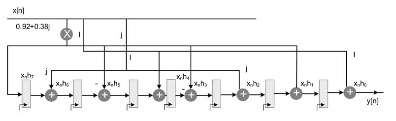
Example: Redesign the architecture of Figure 6.24 using a TDF FIR filter structure. Optimize the multiplications using the CSE technique.
The filter coefficients for N = 8 are computed by evaluating the expression W N n 2 for n = 0… 7.
The values of the coefficients are:

These values of coefficients require just one multiplier and swapping of real and imaginary components of x[n] for realizing multiplication by j. The FIR filter structure of Figure 6.24 is given in Figure 6.25.
Figure 6.25 Optimized TDF implementation of the DF implementation in Figure 6.24
Exercises
Exercise 6.1
Convert the following expression into its equivalent 8-bit fixed-point representation:
Further convert the fixed-point constants into their respective CSD representations. Consider x[n] is an 8-bit input in Q1.7 format. Draw an RTL diagram to represent your design. Each multiplication should be implemented as a CSD multiplier. Consider only the four most significant non-zero bits in your CSD representation.
Exercise 6.2
Implement the following difference equation in hardware:
First convert the constant to appropriate 8-bit fixed-point format, and then convert fixed-point number in CSD representation. Implement CSD multipliers and code the design in RTL Verilog.
Exercise 6.3
Draw an optimal architecture that uses a CSD representation of each constant with four non-zero bits. The architecture should only use one CPA outside the filter structure of Figure 6.26.
Figure 6.26 Design for exercise 6.3
Exercise 6.4
Optimize the hardware design of a TDF FIR filter with the following coefficients in fixed-point format:
Minimize the number of adder levels using sub-graph sharing and CSE techniques.
Exercise 6.5
In the following matrix of constant multiplication by a vector, design optimized HW using a CSE technique:
Exercise 6.6
Compute the dot product of two vectors A and x, where A is a vector of constants and x is a vector of variable data with 4-bit elements. The coefficients of A are:
Use symmetry of the coefficients to optimize the DA-based architecture. Test the design for the following:
Exercise 6.7
Consider the following nine coefficients of an FIR filter:
h[n] = [—0:0456 —0:1703 0:0696 0:3094 0:4521 0:3094 0:0696 —0:1703 —0:0456]
Convert the coefficients into Q1.15 format. Consider x[n] to be an 8-bit number. Design the following DA-based architecture:
1.a unified ROM-based design;
2.reduced size of ROM by the use of symmetry of the coefficients;
3.a DA architecture based on three parallel sub-filters;
4.a ROM-less DA-based architecture
Exercise 6.8
A second-order IIR filter has the following coefficients:
1. Convert the coefficients into 16-bit fixed-point numbers.
2. Design a DA-based architecture that uses a unified ROM as LUT. Consider x[n] to be an 8-bit number. Use two LUTs, one for feedback and the other for feedforward coefficients.
Exercise 6.9
The architecture of Figure 6.24 computes the DFT of an 8-point sequence using convolution summation. Replace the DF FIR structure in the architecture with a TDF filter structure. Exploit the symmetry in the coefficients and design architecture by minimizing multipliers and ROM size. Draw an RTL diagram and write Verilog code to implement the design. Test the design using a 16-bit complex input vector of eight elements. Select an appropriate Q-format for the architecture, and display your result as 16-bit fixed-point numbers.
References
1.Avizienis, “Signed-digit number representation for fast parallel arithmetic,” IRE Transactions on Electronic Computers, 1961, vol. 10, pp. 389–400.
2.R. Hashemian, “A new method for conversion of a 2’s complement to canonic signed digit number system and its representation,” in Proceedings of 30th IEEE Asilomar Conference on Signals, Systems and Computers , 1996, pp. 904–907.
3.H. H. Loomisand B. Sinha, “High-speed recursive digital filter realization,” Circuits, Systems and Signal Processing , 1984, vol. 3, pp. 267–294.
4.K. K. Parhi and D. G. Messerschmitt, “Pipeline interleaving parallelism in recursive digital filters. Pt I: Pipelining using look-ahead and decomposition,” IEEE Transactions on Acoustics, Speech Signal Processing , 1989, vol. 37, pp. 1099–1117.
5.K. K. Parhi and D. G. Messerschmitt, “Pipeline interleaving and parallelism in recursive digital filters. Pt II: Pipelining incremental block filtering,” IEEE Transactions on Acoustics, Speech Signal Processing , 1989, vol. 37, pp. 1118–1134.
6.A. V. Oppenheim and R. W. Schafer, Discrete-time Signal Processing , 3rd, 2009, Prentice-Hall.
7.Y. C. Lim and S. R. Parker, “FIR filter design over a discrete powers-of-two coefficient space,” IEEE Transactions on Acoustics, Speech Signal Processing , 1983, vol. 31, pp. 583–691.
8.H. Samueli, “An improved search algorithm for the design of multiplierless FIR filters with powers-of-two coefficients,” IEEE Transactions on Circuits and Systems, 1989, vol. 36, pp. 1044–1047.
9.J.-H. Han and I.-C. Park, “FIR filter synthesis considering multiple adder graphs for a coefficient,” IEEE Transactions on Computer-Aided Design of Integrated Circuits and Systems , 2008, vol. 27, pp. 958–962.
10.A. G. Dempster. and M. D. Macleod, “Use of minimum-adder multiplier blocks in FIR digital filters,” IEEE Transactions on Circuits and Systems II, 1995, vol. 42, pp. 569–577.
11.J.-H. Han and I.-C. Park, “FIR filter synthesis considering multiple adder graphs for a coefficient,” IEEE Transactions on Computer-Aided Design of Integrated Circuits and Systems , 2008, vol. 27, pp. 958–962.
12.R. I. Hartley, “Subexpression sharing in filters using canonic signed digit multipliers,” IEEE Transactions on Circuits and Systems II, 1996, vol. 43, pp. 677–688.
13.S.-H. Yoon, J.-W. Chong and C.-H. Lin, “An area optimization method for digital filter design,” ETRI Journal , 2004, vol. 26, pp. 545–554.
14.Y. Jang. and S. Yang, “Low-power CSD linear phase FIR filter structure using vertical common sub-expression,” Electronics Letters , 2002, vol. 38, pp. 777–779.
15.A. P. Vinod, E. M.-K. Lai, A. B. Premkuntar and C. T. Lau, “FIR filter implementation by efficient sharing of horizontal and vertical sub-expressions,” Electronics Letters , 2003, vol. 39, pp. 251–253.
16.S. B. Slimane, “Reducing the peak-to-average power ratio of OFDM signals through precoding,” IEEE Transactions on Vehicular Technology , 2007, vol. 56, pp. 686–695.
17.A. Hosnagadi, F. Fallah and R. Kastner, “Common subexpression elimination involving multiple variables for linear DSP synthesis,” in Proceedings of 15th IEEE International Conference on Application-specific Systems, Architectures and Processors , Washington 2004, pp. 202–212.
18.D. J.Allred, H.Yoo, V.Krishnan, W.Huang andD.V.Anderson, “LMS adaptivefilters using distributed arithmetic for high throughput,” IEEE Transactions on Circuits and Systems , 2005, vol. 52, pp. 1327–1337.
19.P. K. Meher, S. Chandrasekaran and A. Amira, “FPGA realization of FIR filters by efficient and flexible systolization using distributed arithmetic,” IEEE Transactions on Signal Processing, 2008, vol. 56, pp. 3009–3017.
20.W. Sen, T. Bin and Z. Jim, “Distributed arithmetic for FIR filter design on FPGA,” in Proceedings of IEEE international conference on Communications, Circuits and Systems , Japan, 2007, vol. 1, pp. 620–623.
21.S. A. White, “Applications of distributed arithmetic to digital signal processing: a tutorial review,” IEEE ASSP Magazine , 1989, vol. 6, pp. 4–19.
22.P. Longa and A. Miri, “Area-efficient FIR filter design on FPGAs using distributed arithmetic,” Proceedings of IEEE International Symposium on Signal Processing and Information Technology , 2006, pp. 248–252.
23.S. Hwang, G. Han, S. Kang and J. Kim, “New distributed arithmetic algorithm for low-power FIR filter implementation,” IEEE Signal Processing Letters, 2004, vol. 11, pp. 463–466.
24.H. Yoo and D. V. Anderson, “Hardware-efficient distributed arithmetic architecture for high-order digital filters,” Proceedings of IEEE International Conference on Acoustics, Speech and Signal Processing , 2005, vol. 5, pp. 125–128.
25.H.Natarajan,A.G. Dempster andU.Meyer-B€ase, “Fast discrete Fourier transform computations using the reduced adder graph technique,” EURASIP Journal on Advances in Signal Processing , 2007, December, pp. 1–10.