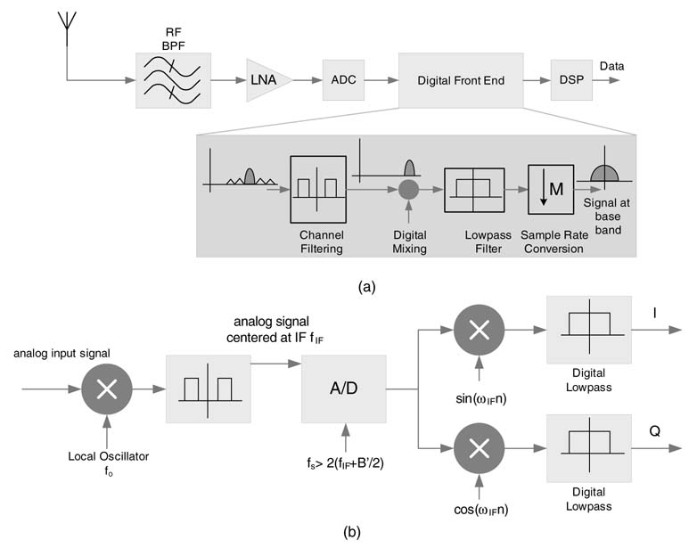
In many designs the analog signal is first translated to a common intermediate frequency fIF. The signal is also filtered to remove images and harmonics. The highest frequency content of this signal is fIF+ B’/2, where B’is the bandwidth of the filtered signal with components of the adjacent channels still part of the signal. Applying Nyquist, the signal can be digitized at twice this frequency. The sampling frequency in this case needs to be greater than 2 (fIF + B’/2). The digital signal is then digitally mixed using a quadrate mixer, and low-pass filters then remove adjacent channels from the quadrate I and Q signals. The signal is then decimated to only keep the required number of samples at base band. A typical receiver that digitizes a signal centered at fIF for further processing is shown in Figure 8.3(b).
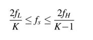
where, for minimum sampling frequency that avoids any aliasing, the maximum value of Kislower-bounded by:
This relationship usually makes the system operate ‘on the edge’, so care must be exercised to relax the condition of sampling frequency such that the copies of the aliased spectrum must fall with some guard bands between two copies. The sampling frequency options for different values of K are given in [1].
It is important to point out that, athough the sampling rate is the fastest frequency at which an A/D converter can sample an analog signal, the converter’s bandwidth (BW) is also an important consideration. This corresponds to the highest frequency at which the internal electronics of the converter can pass the signal without any attenuation. The Nyquist filter at the front of the A/D converter should also be a band-pass filtered and must clean the unused part of the original spectrum for intentional aliasing for band-pass sampling.
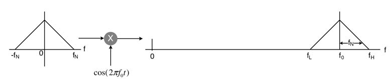
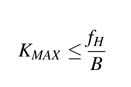
Example: Consider a signal at the front end of a digital communication receiver occupying a bandwidth of 20 MHz and centered at 80 MHz IF. To sample the signal at Nyquist rate requires an A/D to sample the signal at a frequency greater than 180 MHz and the front end to process these samples every second. The band-pass sampling technique can relax this stringent constraint by sampling the signal at a much lower rate. Using expressions (8.1) and (8.2), many options can be evaluated for feasible band-pass sampling. The signal is sampled at 65 MHz for intentional aliasing in a non-overlapping band of the spectrum.A spectrum of the hypothetical original signal centered at 80 MHz and spectrum of its sampled version are given in Figure 8.4.
8.4 Unfolding Techniques
8.4.1 Loop Unrolling
In the software context, unfolding transformation is the process of ‘unrolling’ a loop so that several iterations of the loop are executed in one unrolled iteration. For this reason, unfolding is also called ‘loop unrolling’. It is a technique widely used by compilers for reducing the loop overhead in code written in high-level languages. For hardware design, unfolding corresponds to applying a mathematical transformation on a dataflow graph to replicate its functionality for computing multiple output samples for given relevant multiple input samples. The concept can also be exploited while performing SW to HW mapping of an application written in a high-level language. Loop unrolling gives more flexibility to the HW designer to optimize the mapping. Often the loop is not completely unrolled, but unfolding is performed to best use the HW resources, retiming and pipelining.
Loop unrolling can be explained using a dot-product example. The following code depicts a dot-product computation of two linear arrays of size N:
sum=0;
for (I=0; I<N; I++)
sum += a[I]*b[I];
For computing each MAC (multiplication and accumulation) operation, the program executes a number of cycles to maintain the loop; this is known as the loop overhead. This overhead includes incrementing the counter variable I and comparing the incremented value with N, and then taking a branch decision to execute or not to execute the loop iteration. In addition to this, many DSPs have more than one MAC unit. To reduce the loop overhead and to utilize the multiple MAC units in the DSP architecture, the loop can be unrolled by a factor of J. For example, while mapping this code on a DSP with four MAC units, the loop should first be unrolled for J = 4. The unrolled loop is given here:
J=4
sum1=0
sum2=0;
sum3=0;
sum4=0;
for(I=0; I<N; I=I+J)
{
 sum1 += a[I]*b[I];
 sum2 += a[i+1]*b[i+1];
 sum3 += a[i+2]*b[i+2];
 sum4 += a[i+3]*b[i+3];
}
Similarly, the same loop can be unrolled by any factor J depending on the value of loop counter N and the number of MAC units on a DSP. In software loop unrolling, a designer is trading off code size with performance.
8.4.2 Unfolding Transformation
Algorithms for unfolding a DFG are available [5-8]. Any DFG can be unfolded by an unfolding factor J using the following two steps:
S0 To unfold the graph, each node U of the original DFG is replicated J times as U0, . . . ,UJ- 1 in the unfolded DFG.
S1 For two connected nodes U and Van the original DFG with w delays, draw J edges such that each edge j (= 0… J — 1) connects node Jug to node V(j + w)%J with [(j + w)/J] delays, where % and [.] are, respectively, remainder and floor operators.
Making J copies of each node increases the area of the design many-fold. but the number of delays in the unfolded transformation remains the same as in the original DFG. This obviously increases the critical path delay and the IPB for a recursive DFG by a factor of J.
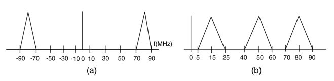
Example: This example applies the unfolding transformation for an unfolding factor of 2 to a second-order IIR filter in TDF structure, shown in Figure 8.5(a). Each node of the DFG is replicated twice and the edges without delays are simply connected as they are. For edges with delays, the step S1 of unfolding transformation is applied. The nodes (U, V) on an edge with one delay in the original DFG are first replicated twice as (U0, U1) and (V0, V1). Now for j = 0 and w= 1, node U0 is connected to node V(0 + 1)%2=1 with delays [(0+ 1)/2] =0; and for j= 1 and w = 1, node U1 is connected to node V(1+1)%2=0 with delays [(1 + 1)/2] = 1. This is drawn by the joining of node U0 to corresponding node V1 with 0 delay and node U1 to corresponding node V0 with 1 delay. Similarly, unfolding is performed on the second edge with a delay and the resultant unfolded DFG is shown in Figure 8.5(b).
8.4.3 Loop Unrolling for Mapping SW to HW
In many applications, algorithms are developed in high-level languages. Their implementation usually involves nested loops. The algorithm processes a defined number of input samples every second. The designer needs to map the algorithm in HW to meet the computational requirements. Usually these requirements are such that the entire algorithm need not to be unrolled, but a few iterations are unrolled for effective mapping. The unfolding should be carefully designed as it may lead to more memory accesses.
Loop unrolling for SW to HW mapping is usually more involved than application of an unfolding transformation on Digs. The code should be carefully analyzed because, in instances with several nested loops, unrolling the innermost loop may not generate an optimal architecture. The architect should explore the design space by unrolling different loops in the nesting and also try merging a few nested loops together to find an effective design.
For example, in the case of a code that filters a block of data using an FIR filter, unrolling the outer loop that computes multiple output samples, rather than the inner loop that computes one output sample, offers a better design option. In this example the same data values are used for computing multiple output samples, thus minimizing the memory accesses. This type of unrolling is difficult to achieve using automatic loop unrolling techniques. The following example shows an FIR filter implementation that is then unrolled to compute four output samples in parallel:
 #include <stdio.h>
 #define N 12
 #define L 8
// Test data and filter coefficients
short be[N+L-1]={1, 1, 2, 3, 4, 1, 2, 3, 1, 2, 1, 4, 5, -1, 2, 0, 1, -2, and 3};
short huff[L]={5, 9, -22, 11, 8, 21, 64, 18};
short by[N];
// The function performs block filtering operation
void BlkFilter(short *xptr, short *hptr, int len_x, int len_h, short *ybf)
{
 int n, k, m;
 for (n=0; n<len_x; n++)
 {
 sum = 0;
 for(k=0, m=n; k<len_h; k++, m–)
 sum += xptr[m]*hptr[k]; // MAC operation
 ybf[n] = sum;
 }
}
// Program to test BlkFilter and BlkFilterUnroll functions void main(void)
{
 short *xptr, *hptr;
 xptr = &[L-1]; //  xbf  has L-1 old samples
 hptr =  hbf ;
 BlkFilterUnroll (xptr, hptr, N, L, ybf);
 BlkFilter (xptr, hptr, N, L, ybf);
}
The unrolled loop for effective HW mapping is given here:
// Function unrolls the inner loop to perform 4 MAC operations
// while performing block filtering function
void BlkFilterUnroll(short *xptr, short *hptr, int len_x, int len_h, short *ybf)
{
 short sum_n_0, sum_n_1, sum_n_2, sum_n_3;
 int n, k, m;
 // Unrolling outer loop by a factor of 4
 for (n=4-1; n<len_x; n+=4)
 {
  sum_n_0 = 0;
  sum_n_1 = 0;
  sum_n_2 = 0;
  sum_n_3 = 0;
 for (k=0, m=n; k<len_h; k++, m–)
 {
  sum_n_0 += hptr[k] * xptr[m];
  sum_n_1 += hptr[k] * xptr[m-1];
  sum_n_2 += hptr[k] * xptr[m-2];
  sum_n_3 += hptr[k] * xptr[m-3];
 }
 ybf[n] = sum_n_0;
 ybf[n-1] = sum_n_1;
 ybf[n-2] = sum_n_2;
 ybf[n-3] = sum_n_3;
 }
 }
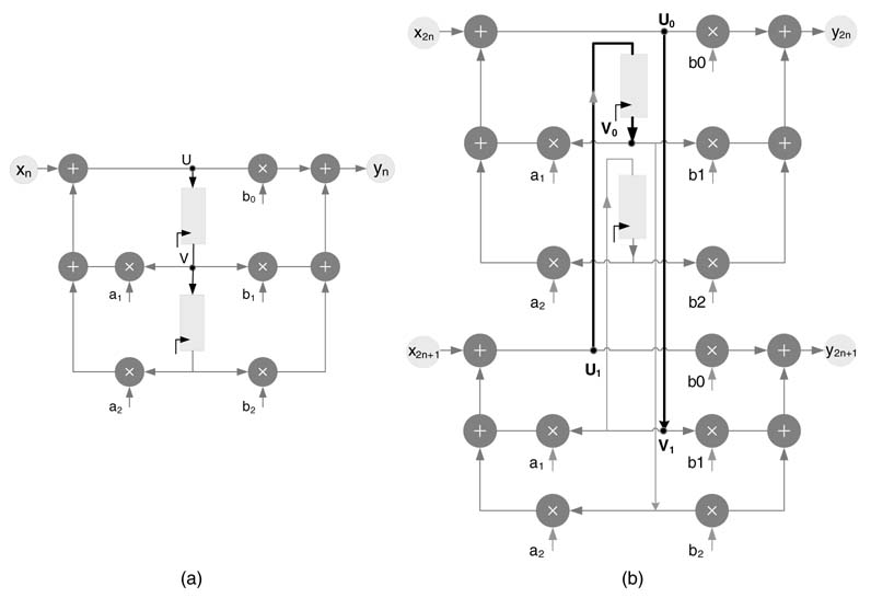
The code processes N input samples in every iteration to compute N output samples in L iterations of the innermost loop. The processing of the innermost loop requires the previous L— 1 input samples for computation of convolution summation. All the required input samples are stored in a buffer xbf of size N+L— 1. The management of the buffer is conveniently performed using circular addressing, where every time N new input data values are written in the buffer replacing the oldest N values. This arrangement always keeps the L— 1 most recent previous values in the buffer.
Figure 8.6 shows mapping of the code listed above in hardware with four MAC and three delay registers. This architecture only requires reading just one operand each from xbf and hbf memories. These values are designated as x[m] and y[k]. At the start of every iteration the address registers for xbf and hbf are initialized to m=L+4—1 and k= 0, respectively. In every cycle address, register m is decremented and k is incremented by 1. In L cycles the architecture computes four output samples. The address m is then incremented for the next iteration of the algorithm. Three cycles are initially required to fill the tap delay line. The architecture can be unfolded to compute as many output samples as required and still needs to read only one value from each buffer.
There is no trivial transformation or loop unrolling technique that automatically generates such an optimized architecture. The designer’s intellect and skills are usually required to develop an optimal architecture.
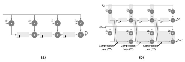
8.4.4 Unfolding to Maximize Use of a Compression Tree
For hardware design of feedforward DFGs, effective architectural options can be explored using unfolding transformation. An unrolled design processes multiple input samples by using
It is important to point out that the design can also be pipelined for effective throughput increase. In many designs, simple pipelining without any folding may cost less in terms of HW than unfolding, because unfolding creates a number of copies of the entire design.
8.4.5 Unfolding for Effective Use of FPGA Resources
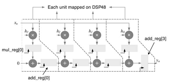
Consider a design instance where the through put is required to be increased by a factor of 2. Assume the designer is using an FPGA with embedded DSP48 blocks. The designer can easily add additional pipeline registers and retime them between a multiplier and an adder, as shown in Figure 8.8 . The Virology code of the pipelined and non-pipelined 4-coefficient TDF FIR implementation is given here:
/* Simple TDF FIR implementation without pipelining /
module FIR Filter
(
input calk,
input signed [15:0] an, // Input data in Q1.15
output signed [15:0] yen); // Output data in Q1.15
// All coefficients of the FIR filter are in Q1.15 format
parameter signed [15:0] h0 = 16b1001100110111011;
parameter signed [15:0] h1 = 16b1010111010101110;
parameter signed [15:0] h2 = 16b0101001111011011;
parameter signed [15:0] h3 = 16b0100100100101000;
rag signed [31:0] adore[0:2]; // Transpose Direct Form delay line
wire signed [31:0] pullout[0:4]; // Wires for intermediate results
always @(posed calk)
begin
 // TDF delay line
 adore[0] <= pullout[0];
 adore[1] <= pullout[1]+adore[0];
 adore[2] <= pullout[2]+adore[1];
end
 assign pullout[0]= an * h3;
 assign pullout[1]= an * h2;
 assign pullout[2]= an * h1;
 assign pullout[3]= an * h0;
 assign pullout[4] = pullout[3]+adore[2];
 // Quantizing it back to Q1.15 format
 assign yen = pullout[4][31:16];
end module
/* Pipelined TDF implementation of a 4-coefficient FIR filter for effective mapping on embedded DSP48 based FPGAs/
module FIRFilterPipeline
(
input clk,input signed [15:0] xn, // Input data in Q1.15 output signed [15:0] yn);
// Output data in Q1.15
// All coefficients of the FIR filter are in Q1.15 format
parameter signed [15:0] h0 = 16b1001100110111011;
parameter signed [15:0] h1 = 16b1010111010101110;
parameter signed [15:0] h2 = 16b0101001111011011;
parameter signed [15:0] h3 = 16b0100100100101000;
reg signed [31:0] add_reg[0:2]; // Transposed direct-form delay line
reg signed [31:0] mul_reg[0:3]; // Pipeline registers
wire signed [31:0] yn_f; // Full-precision output
always @(posedge clk)
begin
 // TDF delay line and pipeline registers
 add_reg[0] <= mul_reg[0];
 add_reg[1] <= mul_reg[1]+add_reg[0];
 add_reg[2] <= mul_reg[2]+add_reg[1];
 add_reg[3] <= mul_reg[3]+add_reg[2];
 mul_reg[0] <= xn*h3;
 mul_reg[1] <= xn*h2;
 mul_reg[2] <= xn*h1;
 mul_reg[3] <= xn*h0;
end
 // Full-precision output
 assign yn_f = mul_reg[3];
 // Quantizing to Q1.15
 assign yn = yn_f[31:16];
endmodule
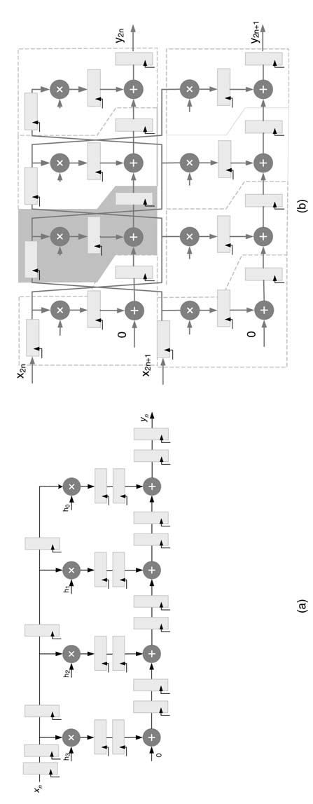
When the requirement on throughput is almost twice what is achieved through one stage of pipelining and mapping on DSP48, will obviously not improve the throughput any further. In these cases unfolding can become very handy. The designer can add pipeline registers as shown in Figure 8.9(a). The number of pipeline registers should be such that each computational unit must have two sets of registers. The DFG is unfolded and the registers are then retimed and appropriately placed for mapping on DSP48 blocks.In the example shown the pipeline DFG is unfolded by a factor of 2. Each pipelined MAC unit of the unfolded design can then be mapped on a DSP48 where the architecture processes two input samples at a time. The pipeline DFG and its unfolded design are shown in Figure 8.9(b). The mapping on DSP48 units is also shown with boxes with one box shaded in gray for easy identification. The RTL Verilog code of the design is given here:
/* Pipelining then unfolding for effective mapping on
DSP48-based FPGAs with twice speedup/
module FIRFilterUnfold
(
input clk,
input signed [15:0] xn1, xn2, // Two inputs in Q1.15
output signed [15:0] yn1, yn2); // Two outputs in Q1.15
// All coefficients of the FIR filter are in Q1.15 format
parameter signed [15:0] h0 = 16’b1001100110111011;
parameter signed [15:0] h1 = 16’b1010111010101110;
parameter signed [15:0] h2 = 16’b0101001111011011;
parameter signed [15:0] h3 = 16’b0100100100101000;
// Input sample tap delay line for unfolding design
reg signed [15:0] xn_reg[0:4];
// Pipeline registers for first layer of multipliers
reg signed [31:0] mul_reg1[0:3];
// Pipeline registers for first layer of adders
reg signed [31:0] add_reg1[0:3];
// Pipeline registers for second layer of multipliers
reg signed [31:0] mul_reg2[0:3];
// Pipeline registers for second layer of adders
reg signed [31:0] add_reg2[0:3];
// Temporary wires for first layer of multiplier results
wire signed [31:0] mul_out1[0:3];
// Temporary wires for second layer of multiplication results
wire signed [31:0] mul_out2[0:3];
always @(posedge clk)
begin
 // Delay line for the input samples
 xn_reg[0] <= xn1;
 xn_reg[4] <= xn2;
 xn_reg[1] <= xn_reg[4];
 xn_reg[2] <= xn_reg[0];
 xn_reg[3] <= xn_reg[1];
end
always @(posedge clk)
begin
 // Registering the results of multipliers
 mul_reg1[0] <= mul_out1[0];
 mul_reg1[1] <= mul_out1[1];
 mul_reg1[2] <= mul_out1[2];
 mul_reg1[3] <= mul_out1[3];
 mul_reg2[0] <= mul_out2[0];
 mul_reg2[1] <= mul_out2[1];
 mul_reg2[2] <= mul_out2[2];
 mul_reg2[3] <= mul_out2[3];
end
always @(posedge clk)
begin
 // Additions and registering the results
 add_reg1[0] <= mul_reg1[0];
 add_reg1[1] <= add_reg1[0]+mul_reg1[1];
 add_reg1[2] <= add_reg1[1]+mul_reg1[2];
 add_reg1[3] <= add_reg1[2]+mul_reg1[3];
 add_reg2[0] <= mul_reg2[0];
 add_reg2[1] <= add_reg2[0]+mul_reg2[1];
 add_reg2[2] <= add_reg2[1]+mul_reg2[2];
 add_reg2[3] <= add_reg2[2]+mul_reg2[3];
end
 // Multiplications
 assign mul_out1[0]= xn_reg[0] * h3;
 assign mul_out1[1]= xn_reg[1] * h2;
 assign mul_out1[2]= xn_reg[2] * h1;
 assign mul_out1[3]= xn_reg[3] * h0;
 assign mul_out2[0]= xn_reg[4] * h3;
 assign mul_out2[1]= xn_reg[0] * h2;
 assign mul_out2[2]= xn_reg[1] * h1;
 assign mul_out2[3]= xn_reg[2] * h0;
 // Assigning output in Q1.15 format
 assign yn1 = add_reg1[3][31:16];
 assign yn2 = add_reg2[3][31:16];
endmodule
8.4.6 Unfolding and Retiming in Feedback Designs
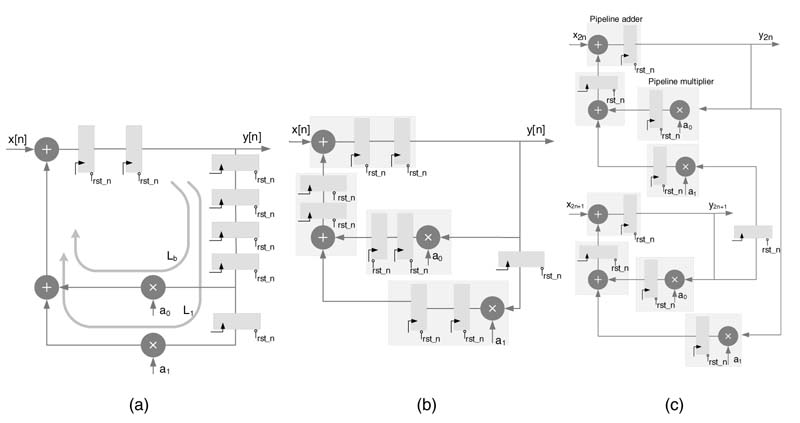
It has already been established that an unfolding transformation does not improve timing; rather, it results in an increase in critical path delay and, for feedback designs, an increase in IPB by the Unfolding and retiming of a feedback DFG. (a) Recursive DFG with seven algorithmic registers. (b) Retiming of resisters for associating algorithmic registers with computational nodes for effective unfolding. (c) Unfolded design for optimal utilization of algorithmic registers unfolding factor J. This increase is because, although all the computational nodes are replicated J times, still the number of registers in the unfolded DFG remains the same. For feedback designs, unfolding may be effective for design instances where there are abundant algorithmic registers for pipelining the combinational nodes in the design. In these designs, unfolding followed by retiming provides flexibility of placing these algorithmic registers in the unfolded design while optimizing timing. Similarly for feedforward designs, first pipeline registers are added and the design is then unfolded and retimed for effective placement of registers, as explained in Section 8.4.5.
The registers in DFGs can be retimed for effective pipelining of the combinational cloud. In cases where the designer is using embedded computational units or computational units with limited pipeline support, there may exist extra registers that are not used for reducing the critical path of the design. In these designs the critical path is greater than IPB. For example, the designer might intend to use already embedded building blocks on an FPGA like DSP48. These blocks have a fixed pipeline option and extra registers do not help in achieving the IPB. By unfolding and retiming, the unfolded design can be appropriately mapped on the embedded blocks to effectively use all the registers.
The registers can be retimed such that each computational unit has two registers to be used as pipeline registers, as shown in Figure 8.10(b). The design is unfolded and registers are retimed for optimal HW mapping, as shown in Figure 8.10(c). The RTL Verilog code of the three designs is listed here:
/* IIR filter of Fig. 8.10(a), having excessive algorithmic registers/
module IIRFilter
(
input clk, rst_n, input signed [15:0] xn, //Q1.15
output signed [15:0] yn); //Q1.15
parameter signed [15:0] a0=16’b0001_1101_0111_0000;
 //0.23 in Q1.15
parameter signed [15:0] a1=16’b1100_1000_1111_0110;
 //=0.43 in Q1.15
reg signed [15:0] add_reg[0:1];
reg signed [15:0] y_reg[0:3]; // Input sample delay line
reg signed [15:0] delay;
wire signed [15:0] add_out[0:1];
wire signed [31:0] mul_out[0:1];
always @(posedge clk or negedge rst_n)
begin
  if(!rst_n) // Reset all the registers in the feedback loop
  begin
    add_reg[0] <= 0;
    add_reg[1] <= 0;
    y_reg[0] <= 0;
    y_reg[1] <= 0;
    y_reg[2] <= 0;
    y_reg[3] <= 0;
    delay <= 0;
  end
  else
  begin
    // Assign values to registers
    add_reg[0] <= add_out[0];
    add_reg[1] <= add_reg[0];
    y_reg[0] <= yn;
    y_reg[1] <= y_reg[0];
    y_reg[2] <= y_reg[1];
    y_reg[3] <= y_reg[2];
    delay <= y_reg[3];
  end
end
  // Implement combinational logic of two additions and
   two multiplications
  assign add_out[0] = xn + add_out[1];
  assign mul_out[0]= y_reg[3] * a0;
  assign mul_out[1]= delay * a1;
  assign add_out[1] = mul_out[1][31:16]+mul_out[0][31:16];
  assign yn = add_reg[1];
endmodule
/* Retime the algorithmic registers to reduce the critical
 path while mapping the design on FPGAs with DSP48-like blocks /
module IIRFilterRetime
(
input clk, rst_n,
input signed [15:0] xn, //Q1.15
output signed [15:0] yn); //Q1.15
parameter signed [15:0] a0 = 16’b0001_1101_0111_0000;
            //0.23 in Q1.15
parameter signed [15:0] a1 = 16’b1100_1000_1111_0110;
            //=0.43 in Q1.15
reg signed [15:0] mul0_reg[0:1];
reg signed [15:0] mul1_reg[0:1]; // Input sample delay line
reg signed [15:0] add1_reg[0:1];
reg signed [15:0] add0_reg[0:1];
reg signed [15:0] delay;
wire signed [15:0] add_out[0:1];
wire signed [31:0] mul_out[0:1];
// Block Statements
always @(posedge clk or negedge rst_n)
if(!rst_n) // Reset registers in the feedback loop
  begin
     add0_reg[0] <= 0;
     add0_reg[1] <= 0;
     mul0_reg[0] <= 0;
     mul0_reg[1] <= 0;
     mul1_reg[0] <= 0;
     mul1_reg[1] <= 0;
     add1_reg[0] <= 0;
     add1_reg[1] <= 0;
     delay <= 0;
  end
else
  begin
     // Registers are retimed to reduce the critical path
     add0_reg[0] <= add_out[0];
     add0_reg[1] <= add0_reg[0];
     mul0_reg[0] <= mul_out[0][31:16];
     mul0_reg[1] <= mul0_reg[0];
     mul1_reg[0] <= mul_out[1][31:16];
     mul1_reg[1] <= mul1_reg[0];
     add1_reg[0] <= add_out[1];
     add1_reg[1] <= add1_reg[0];
     delay <= yn;
  end
  // Combinational logic implementing additions
     and multiplications
  assign add_out[0]= xn + add1_reg[1];
  assign mul_out[0]= yn * a0;
  assign mul_out[1]= delay * a1;
  assign add_out[1]= mul0_reg[1]+mul1_reg[1];
  assign yn = add0_reg[1];
  endmodule
/* Unfolding and retiming to fully utilize the algorithmic registers for reducing the critical path
   of the design for effective mapping on DSP48-based FPGAs /
module IIRFilterUnfold
(
input clk, rst_n,
input signed [15:0] xn0, xn1, // Two inputs in Q1.15
output signed [15:0] yn0, yn1); //Two outputs in Q1.15
parameter signed [15:0] a0=16’b0001_1101_0111_0000;
    //0.23 in Q1.15
parameter signed [15:0] a1=16’b1100_1000_1111_0110;
   //=0.43 in Q1.15
reg signed [15:0] mul0_reg[0:1];
reg signed [15:0] mul1_reg[0:1]; // Input sample delay line
reg signed [15:0] add1_reg[0:1];
reg signed [15:0] add0_reg[0:1];
reg signed [15:0] delay;
wire signed [15:0] add0_out[0:1], add1_out[0:1];
wire signed [31:0] mul0_out[0:1], mul1_out[0:1];
// Block Statements
always @(posedge clk or negedge rst_n)
if(!rst_n)
  begin
    add0_reg[0] <= 0;
    add0_reg[1] <= 0;
    mul0_reg[0] <= 0;
    mul0_reg[1] <= 0;
    mul1_reg[0] <= 0;
    mul1_reg[1] <= 0;
    add1_reg[0] <= 0;
    add1_reg[1] <= 0;
    delay <= 0;
  end
else
  begin
    // Same number of algorithmic registers, retimed differently
    add0_reg[0] <= add0_out[0];
    add1_reg[0] <= add0_out[1];
    mul0_reg[0] <= mul0_out[0][31:16];
    mul1_reg[0] <= mul0_out[1][31:16];
    add0_reg[1] <= add1_out[0];
    add1_reg[1] <= add1_out[1];
    mul0_reg[1] <= mul1_out[0][31:16];
    mul1_reg[1] <= mul1_out[1][31:16];
    delay <= yn1;
  end
  /* Unfolding by a factor of 2 makes two copies of the
    combinational nodes/
  assign add0_out[0]= xn0 + add1_reg[0];
  assign mul0_out[0]= yn0 * a0;
  assign mul0_out[1]= delay * a1;
  assign add0_out[1]= mul0_reg[0]+mul1_reg[0];
  assign yn0 = add0_reg[0];
  assign add1_out[0]= xn1 + add1_reg[1];
  assign mul1_out[0]= yn1 * a0;
  assign mul1_out[1]= yn0 * a1;
  assign add1_out[1]= mul0_reg[1]+mul1_reg[1];
  assign yn1 = add0_reg[1];
endmodule
module testIIRfilter;
reg signed [15:0] Xn, Xn0, Xn1;
reg RST_N, CLK, CLK2;
wire signed [15:0] Yn, Yn0, Yn1;
wire signed [15:0] Yn_p;
integer i;
// Instantiating the two modules for equivalence checking
IIRFilterIIR(CLK, RST_N, Xn, Yn);
IIRFilterRetime IIRRetime(CLK, RST_N, Xn, Yn_p);
IIRFilterUnfoldIIRUnfold(CLK2, RST_N, Xn0, Xn1, Yn0, Yn1);
initial
begin
CLK = 0; // Sample clock
CLK2 = 0;
Xn = 215;
Xn0 = 215;
Xn1 = 430;
#1 RST_N =1; // Generate reset
#1 RST_N = 0;
#3 RST_N = 1; end
// Generating clock signal always
#4 CLK = ~CLK; // Sample clock // Generating clock signal for unfolded module always
#8 CLK2 = ~CLK2; // Twice slower clock always @(posedge CLK) begin
Xn <= Xn+215; end
always @(posedge CLK2) begin
Xn0 <= Xn0+430;
Xn1 <= Xn1+430; end initial
$monitor ($time, " Yn=%d, Yn_p=%d, Yn0=%d, Yn1=%d
", Yn, Yn_p, Yn0, Yn1);
endmodule
8.5 Folding Techniques
Chapter 9 covers time-shared architectures. These are employed when the circuit clock is at least twice as fast as the sampling clock. The design running at circuit clock speed can reuse its hardware resources because the input data remains valid for multiple circuit clocks. In many design problems the designer can easily come up with time-shared architecture. Examples in Chapter 9 highlight a few of the design problems. For complex applications, designing an optimal time-shared architecture is a complex task. This section also covers a mathematical technique for designing time-shared architectures.
8.5.1 Definitions and the Folding Transformation
- Folding is a mathematical technique for finding a time-multiplexed architecture and a schedule of mapping multiple operations of a dataflow graph on fewer hardware computational units.
- The foldingfactor is defined as the maximum number of operations in a DFG mapped on a shared computational unit.
- A foldingset or foldingscheduler is the sequence of operations of a DFG mapped on a single computational unit.
The folding transformation has two parts. The first part deals with finding a folding factor and the schedule for mapping different operations of the DFG on computational units in the folded DFG. The optimal folding factor is computed as:

where fc and fs are circuit and sampling clock frquencies. Based on N and a schedule of mapping multiple operations in the DFG on shared resources, a folded architecture automatically saves intermediate results in registers and inputs them to appropriate units in the scheduled cycle for correct computation.
Folding transformation by a factor of N introduces latency into the system. The corresponding output for an input appears at the output after N clock cycles. The sharing of a computational unit by different operations also requires a controller that schedules these operations in time slots. The controller may simply be a counter, or it can be based on a finite state machine (FSM) that periodically generates a sequence of control signals for the datapath to select correct operands for the computational units.
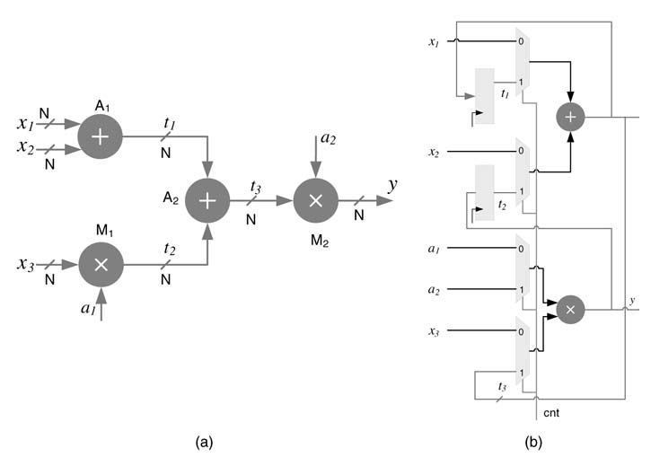
Example: The DFG shown in Figure 8.11(a) is to be folded. The DFG has two nodes (A1 and A2) performing addition and two (M1 nd M2) performing multiplication. Assuming the data is valid for two circuit clock cycles, the DFG is folded by a factor of 2 using one multiplier and one adder. The folded architecture is shown in Figure 8.11(b). The mapping of the algorithm on the folded architecture requires a schedule, which for this example is very simple to work out. For the two cycles ofthe circuit clock, the adder and multiplier perform operations in the order {A1,A2} and {M1, M2}. The folded architecture requires two additional registers to hold the values of intermediate results to be used in the next clock cycle. All the multiplexers select port 0 in the first cycles and port 1 in the second cycle for feeding correct inputs to the shared computational units.
8.5.2 Folding Regular Structured DFGs
Algorithms that exhibit a regular structure can be easily folded. Implementation of an FIR filter is a good example of this. The designer can fold the structure by any order that is computed as the ratio of the circuit and sampling clocks.
For any regularly structured algorithm the folding factor is simply computed as:
(8.3)
The DFG of the regular algorithm is partitioned into Unequal parts. The regularity of the algorithm means implementing the datapath of a single partition as a shared resource. The delay line or temporary results are stored in registers and appropriately input to the shared data path.
Example: An L-coefficient FIR filter implements the convolution equation:
(8.4)
This equation translates into a regularly structured dataflow graph as DF or TDF realizations. The index of summation can be implemented as N summation for k =mM+1, where M =L/N, and the equation can be written as:
(8.5)
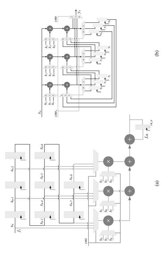
This double summation can be realized as folded architecture. For DF, the inner equation implements the shared resource and the outer equation executes the shared resource N times to compute each output sample y[n]. The realizations of the folded architecture for L=9 and N=3 as DF and TDF are given in Figures 8.12. In the DF case the tap delay line is implemented ‘as is’, whereas the folded architecture implements the inner summation computing 3-coefficient filtering in each cycle. This configuration implements three multipliers and adders as shared resources. The multiplexer appropriately sends the correct inputs to, respectively, multiplier and adder. The adder at the output adds the partial sums and implements the output summation of(8.5).
Figure 8.12(b) shows the TDF realization. Here again all the registers are realized as they are in the FDA implementation whereas the hardware resources are shared. The cntr signal is used to control the multiplexers and demultiplexers to input the correct data to the shared resources and to store the computational results in appropriate registers in each clock cycle.
8.5.3 Folded Architectures for FFT Computation
Most signal processing algorithms have a regular structure. The fast Fourier transform (FFT) is another example to demonstrate the folding technique. An FFT algorithm efficiently implements DFT summation:
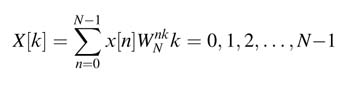
where
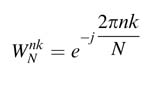
are called twiddle factors . N is the length of the signal x[n], and n and k are the indices in time and frequency, respectively.
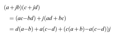
The number of real multiplications required to perform a complex multiplication can be first reduced from four to three by the following simple mathematical manipulation:
There are a variety of algorithmic design options cited in the literature that reduce the number of complex multiplications while implementing (8.6). These options can be broadly divided into two categories: butterfly-based computation and mathematical transformation .
For butterfly-based computation a variety of algorithms based on radix-2, radix-4, radix-8, hybrid radix, radix-22, radix-23, and radix-2/22/23 [9, 10] and a mix of these are proposed. The radix-4 and radix-8 algorithms use fewer complex multiplications than radix-2 but require N to be a power of 4 and 8, respectively. To counter the complexity and still gain the benefits, radix-22 and radix-23 algorithms are proposed in [11] that still use radix-2 type butterflies and reduce the number of complex multiplications. Most of these radix-based algorithms reduce the number of complex multiplications. In general, a radix-r algorithm requires logrN stages of N/r butterflies, and preferably N needs to be a power of r or the data is zero-padded to make the signal of requisite length.
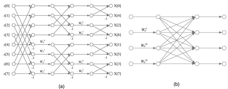
A radix-2 N-point FFT divides the computation into log2N stages where each stage executes N/2 two-point butterflies. A flow graph for 8-point FFT implementation using a radix-2 butterfly is shown in Figure 8.13(a). An 8-point FFT can also be computed by using two stages of radix-4 butterflies, shown in Figure 8.13(b); each stage would contain two of these butterflies.
A pipelined FDA requires the data to be placed at the input of every butterfly in every cycle, and then the design works in lock step to generate N output in every clock cycle with an initial latency of the number of pipeline stages in the design. This design requires placing of N samples at the input of the architecture in every clock cycle. This for large values of N is usually not possible, so then the designer needs to resort to folded architecture.
When there are more clock cycles available for the design,the architecture is appropriately folded. In general, a folded architecture can realize M butterflies in parallel to implement an N-point FFT,
where N=JM and J is the folding factor. The design executes the algorithm in J clock cycles. Feeding the input data to the butterflies and storing the output for subsequent stages of the design is the most critical design consideration. The data movement and storage should be made such that data is always available to the butterflies without any contention. Usually the data is either stored in memory or input to the design using registers. The intermediate results are either stored back in memory or are systematically placed in registers such that they are conveniently available for the next stages of computation. Similarly the output can be stored either in memory or in temporary registers. For register-based architectures the two options are MDC (multi-delay commutator) [12-14] or SDF (single-path delay feedback) [15, 16]. In MDC, feedforward registers and multiplexers are used on r stream of input data to a folded radix- r butterfly.
Figure 8.14 shows a design for 8-point decimation in a frequency FFT algorithm that folds three stages of eight radix-2 butterflies on to three butterflies. The pipeline registers are appropriately placed to fully utilize all the butterflies in all clock cycles.
8.5.4 Memory-based Folded FFT Processor
The designer can also produce a generic FFT processor that uses a number of butterflies in the datapath and multiple dual-ported memories and respective address generation units for computing an N-point FFT [17-19]. Here a memory-based designed is discussed.
For memory-based HW implementation of an N-point radix-2 FFT algorithm, one or multiple butterfly units can be placed in the datapath. Each butterfly is connected to two dual-ported memories and a coefficient ROM for providing input data to the butterfly. The outputs of the butterflies are appropriately saved in memories to be used for the next stages of execution. The main objective of the design is to place input and output data in a way that two corresponding inputs to execute a particular butterfly are always stored in two different dual-port memories. The memory management should be done in a way that avoids access conflicts.
A design using a radix-2 butterfly processing element (PE) with two dual-ported RAMs and a coefficient ROM in the datapath is shown in Figure 8.15(a). While implementing decimation in frequency FFT computation, the design initially stores N/2 points of input data, x0, x1,…, xN/2-1 in
RAM0, and then with the arrival of every new sample, xN/2, xN/2+1, …, xN— 1, executes the following butterfly computations:
(8.7)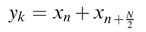
(8.8)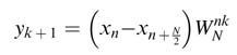
The output of the computations from (8.7) and(8.8) are stored in RAM0 and RAM1, respectively, for the first N/2 samples,and then reversing the storage arrangements whereby the outputs of(8.7) and(8.8) are stored in RAM1 and RAM0, respectively. This arrangement enables the next stage of computation without any memory conflicts.In every stage of FFT computation, the design swaps the storage pattern for every N/2s output samples, where s is the stage of butterfly computation for s = 1, 2,..., log2N.
Example:Figure 8.13(a) shows a flow graph realizing an 8-point decimation in frequency FFT algorithm.The first four samplesofinput,x0...x3, are storedinRAM0.Forthe next input samples the architecture starts executing (8.7) and(8.8)and stores the first four results in RAM0and RAM1,respectively,and the result softhenext four computations are stored in RAM1and RAM0,respectively. This arrangement makes the computation of the next stage of butterfly possible without memory access conflicts. The next stage swaps the storage of results for very two sets of outputs in memories RAM0 and RAM1. The cycle-by-cycle storage of results is shown in Figure 8.13(b).
8.5.5 Systolic Folded Architecture
The FFTalgorithm can also be realized as systolic folded architecture, using an MDF or Debases. In this architecture all the butterflies in one stage of the FFT flow graph are folded and mapped on a single butterfly processing element. To ensure systolic operation, intermediate registers and multiplexers are placed such that the design keeps processing data for computation of FFT and correct inputs are always available to every PE in every clock cycle for full utilization of the hardware.
Implementing the decimation in a frequency FFT algorithm, the architecture requires log2N PEs. To enable fully systolic operation with 100% utilization in the MDF configuration, the two input data streams are provided to PE1. The upper stream serially feeds the first N/2 samples of input data, x0, x1,.. .,xN/2–1, and the lower stream serially inputs the other N/2 samples, xN/2,xN/2+1 ,…,xN— 1. Then PE1 sequentially computes one radix-2 butterfly of decimation in the frequency FFT algorithm in every clock cycle and passes the output to the next stage of folded architecture. To synchronize the input to PE2, the design places a set of N/4 registers each in upper and lower branches. The multiplexers ensure the correct set of data are fed to PE1 and PE2 in every clock cycle. Similarly each stage requires placement of N/2s registers at each input for s=2, 3,…, log2N.
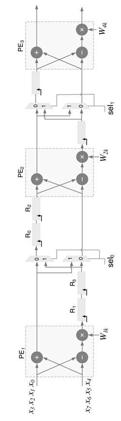
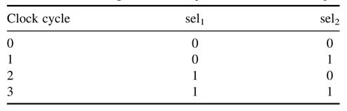
Example:Figure 8.14. shows the details of the design for a systolic FFT implementation. The data is serially fed to PE1 and the output is stored in registers for first two computations of butterfly operations. These outputs are then used for the next two set of computation.
The cycle-by-cycle detailed working of the architecture is shown in Figure 8.16. The first column shows the cycles where the design repeats computation after every fourth cycle and starts computing the 8-point FFT of a new sequence of 8 data points. The second column shows the data being serially fed to the design. The first cycle takes x0 and x4, and then in each subsequent cycle two data values are fed as shown in this column. The columns labeled as PE1, PE2 and PE3 show the butterfly computations. The intermediate values stored in registers R0, R1, R2 and R3 are also shown in the table as yij, where i is the level and j is the index..
The multiplexer selects signals given inTable 8.1. The controller is a simple 2-bit counter, where the most significant bit (MSB) of the counter is used for sel 1 and the least significant bit (LSB) is used for sel2. The counter is used to read the values of twiddle factors from four-deep ROM. The RTL Verilog code is given here:
// Systolic FFT architecture for 8-point FFT computation module FFTSystolic (
input signed [15:0] xi_re, xi_im, xj_re, xj_im, input clk, rst_n,
output signed [15:0] yi_re, yi_im, yj_re, yj_im); reg signed [15:0] R_re[0:5], R_im[0:5]; reg [1:0] counter;
wire signed [15:0] W_re[0:3], W_im[0:3]; // Twiddle factors of three butterflies
reg signed [15:0] W0_re, W0_im, W1_re, W1_im, W2_re, W2_im; wire sel1, sel2;
wire signed [15:0] xj_re1, xj_im1, xj_re2, xj_im2; wire signed [15:0] yi_re1, yi_im1, yj_re1, yj_im1,
yi_re2, yi_im2, yj_re2, yj_im2;
wire signed [15:0] yi_out_re1, yi_out_im1, yi_out_re2,
yi_out_im2; // The control signals assign sel1 = ~counter[1]; assign sel2 = ~counter[0]; // Calling butterfly tasks ButterFly B0(xi_re, xi_im, xj_re, xj_im, W0_re, W0_im,
yi_re1, yi_im1, yj_re1, yj_im1); ButterFly B1(R_re[3], R_im[3], xj_re1, xj_im1, W1_re,
W1_im, yi_re2, yi_im2, yj_re2, yj_im2); ButterFly B2(R_re[5], R_im[5], xj_re2, xj_im2, W2_re,
W2_im, yi_re, yi_im, yj_re, yj_im); Mux2To2 MUX1(yi_re1, yi_im1, R_re[1], R_im[1], sel1,
i_out_re1, yi_out_im1, xj_re1, xj_im1); Mux2To2 MUX2(yi_re2, yi_im2, R_re[4], R_im[4], sel2,
yi_out_re2, yi_out_im2, xj_re2, xj_im2); always @(*) begin
// Reading values of twiddle factors for three butterflies W0_re = W_re[counter]; W0_im = W_im[counter];
W1_re = W_re[{counter[0],1’b0}];W1_im = W_im[{counter[0],1’b0}]; W2_re = W_re[0]; W2_im = W_im[0]; end
always @(posedge clk or negedge rst_n) begin
if(!rst_n) begin
R_re[0] <= 0; R_im[0] <= 0; R_re[1] <= 0; R_im[1] <= 0; R_re[2] <= 0; R_im[2] <= 0; R_re[3] <= 0; R_im[3] <= 0; R_re[4] <= 0; R_im[4] <= 0; R_re[5] <= 0; R_im[5] <= 0; end else begin
R_re[0] <=yj_re1; R_im[0] <=yj_im1; R_re[1] <= R_re[0]; R_im[1] <= R_im[0]; R_re[2] <= yi_out_re1; R_im[2] <= yi_out_im1; R_re[3] <= R_re[2]; R_im[3] <= R_im[2]; R_re[4] <=yj_re2; R_im[4] <=yj_im2; R_re[5] <= yi_out_re2; R_im[5] <= yi_out_im2; end end
always @(posedge clk or negedge rst_n) if(!rst_n)
counter <= 0; else
counter <= counter+1;
// 1, 0
assign W_re[0] =16’h4000; assign W_im[0] =16’h0000;
// 0.707, -0.707
assign W_re[1] = 16’h2D41; assign W_im[1] = 16’hD2BF; // 0, -1
assign W_re[2] = 16’h0000; assign W_im[2] = 16’hC000; // -0.707, -0.707
assign W_re[3] = 16’hD2BF; assign W_im[3] = 16’hD2BF; endmodule
module ButterFly
(
input signed [15:0] xi_re, xi_im, xj_re, xj_im, // Input data
input signed [15:0] W_re, W_im, // Twiddle factors
output reg signed [15:0] yi_re, yi_im, yj_re, yj_im);
// Extra bit to cater for overflow
reg signed [16:0] tempi_re, tempi_im;
reg signed [16:0] tempj_re, tempj_im;
reg signed [31:0] mpy_re, mpy_im;
always @(*)
begin
// Q2.14
tempi_re = xi_re + xj_re; tempi_im = xi_im + xj_im;
// Q2.14
tempj_re = xi_re - xj_re; tempj_im = xi_im - xj_im;
mpy_re = tempj_re*W_re - tempj_im*W_im;
mpy_im = tempj_re*W_im + tempj_im*W_re;
// Bring the output format to Q3.13 for first stage
// and to Q4.12 and Q5.11 for the second and third stages
yi_re = tempi_re>>>1; yi_im = tempi_im>>>1;
// The output for Q2.14 x Q 2.14 is Q4.12
yj_re = mpy_re[30:15]; yj_im = mpy_im[30:15]; end endmodule
module Mux2To2
(
input [15:0] xi_re, xi_im, xj_re, xj_im,
input sel1,
output reg [15:0] yi_out_re, yi_out_im, yj_out_re, yj_out_im);
always @ (*)
begin
if (sel1)
begin yi_out_re = xj_re; yi_out_im = xj_im;
yj_out_re = xi_re; yj_out_im = xi_im; end
else
begin yi_out_re = xi_re; yi_out_im = xi_im;
yj_out_re = xj_re; yj_out_im = xj_im;
end
end endmodule
8.6 Mathematical Transformation for Folding
Many feedforward algorithms can be formulated to recursively compute output samples. DCT [20] and FFT are good examples that can be easily converted to use recursions. Many digital designs for signal processing applications may require folding of algorithms for effective hardware mapping that minimizes area. The folding can be accomplished by using a folding transformation The mathematical formulation of folding transformations is introduced in [21,22]. A brief description is given in this section.
Table 8.1 Select signals for multiplexers of the text example
For a given folding order and a folding set for a DFG, the folding transformation computes the number of delays on each edge in the folded graph. The folded architecture periodically executes operations of the DFG according to the folding set. Figure 8.17 . shows an edge that connects nodes Ui and Vj with Wij delays. The Wij delays on the edge Ui—►Vj signify that the output of node Ui is used by node Vj after Wij cycles or iterations in the original DFG. If the DFG is folded by a folding factor N, then the folded architecture executes each iteration of the DFG in N cycles. All the nodes of type U and vin the DFG are scheduled on computational units Hu and Hv, respectively, in clock cycles ui and vj such that 0≤ui, vi ≤ N–1. If nodes U and Vare of the same type, they may be scheduled on the same computational unit in different clock cycles.
For the folded architecture, node Ui is scheduled in clock cycle ui in the current iteration and node Vj is scheduled in vj clock cycle in the Wij iteration. In the original DFG the output of node Ui is used after Wij clock cycles, and now in the folded architecture, as the node Ui is scheduled in the ui clock cycle of the current iteration and it is used in the Wij iteration in the original DFG, as each iteration takes N clock cycle thus the folded architecture starts executing the Wij iteration in the N × Wij clock cycle, where node Vj is scheduled in the vj clock cycle in this iteration. This implies that, with respect to the current iteration, node Vj is scheduled in the N × Wij+vj clock cycle, so in the folded architecture the result from node Ui needs to be stored for Fij number of register clock cycles, where:
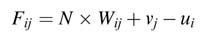
If the node of type U is mapped on a computational unit Hu with Pu pipeline stages, these delays will also be incorporated in the above equation, and the new equation becomes:
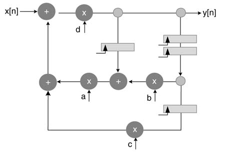
Example: A DFG of second order IIR filter is given in Figure 8.18(a) with three addition nodes 1, 4 and 5, and two multiplication nodes 2 and 3. Fold the architecture by a folding factor of 3 with the folding set for the adder Sa= {4, 5, 1} and the folding set for the multiplier as Sm= {3,_,2}. The number of registers for each edge in the folded architecture using the equation for the folding transformation assuming no pipeline stage in multiplier and adder, is as follows:
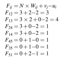
After figuring out the number of registers required for storing the intermediate results, the architecture can be easily drawn. One adder and one multiplier are placed with two sets of 3:1 multiplexers with each functional unit. Now observing the folding set, connections are made from the registers to the multiplier. For example, the adder first executes node 4. This node requires inputs from node 2 and node 1. The values of F24 and F14 are 1 and 1, where node 2 is the multiplier node. The connectionstoport0ofthe two multiplexers at the input of the adder are made by connecting the output of one register after multiplier and one register after adder. Similarly, connections for all the operations are made based on folding set and values of Fij.
The folded design is shown in Figure 8.18(b). The input data is feed to the system every three cycles. The multiplexer selects the input to the functional units, the selected line simply counts from 00 to 10 and starts again from 00.
8.7 Algorithmic Transformation
In many applications a more convenient hardware mapping can be achieved by performing an algorithmic transformation of the design. For FFT computations the Goertzel algorithm is a good example, where the computations are implemented as air filter [23]. This formulation is effective if only a few coefficients of the frequency spectrum are to be computed.
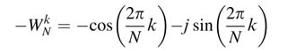
DTMF (dual-tone multi-frequency) is an example where the Goertzel algorithm is widely used. This application requires computation of the frequency content of eight frequencies for detection of dialed digits in telephony. The algorithm takes the formulation of (8.6) and converts it to a convolution summation of an IIR linear time-invariant (LTI) system with the transfer function:
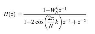
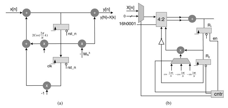
The Nth output sample of the system gives a DFT of N data samples at the kth frequency index. Figure 8.19(a) shows the IIR filter realization of the transfer function. The feedforward path involves a multiplication by—WNK that only needs to be computed at every Nth sample, and the multiplication by—1 and two additions in the feedback loop can be implemented by a compression tree and an adder. The design can be effectively implemented by using just one adder and a multiplier and is shown in Figure 8.19(b). The multiplier is reused for complex multiplication after the Nth cycle.
Assuming real data, 0, 1,…, N—1 cycles compute the feedback loop. In the Nth cycle, the en of register R1 is de-asserted and register R2 is reset. The multiplexer selects multiplier for the multiplication by:
in two consecutive cycles. In these cycles, a zero is fed in the compressor for x[n].
Exercises
Exercise 8.1
A 4 MHz bandwidth signal is centered at an intermediate frequency of 70 MHz. Select the sampling frequency of an ADC that can band pass sample the signal without any aliasing.
Exercise 8.2
The mathematical expression for computing correlation of a mask m[n1, n2] of dimensions L1xL2 with an image I[n1, n2] of size N1xN2 is:
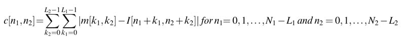
Write C code to implement the nested loop that implements the correlation summation. Assuming L1 = L2 = 3and N1 =N2 = 256, unroll the loops to speedup the computationbyafactorof9such that the architecture needs to load the minimum number of new image samples and maximize data reuse across iterations.
Exercise 8.3
A 48th-order IIR filter is given by the following mathematical expression:
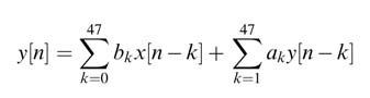
Write C code to implement the equation. Design a folded architecture by appropriately unrolling loops in C implementation of the code. The design should perform four MAC operations of the feed forward and four MAC operations of the feedback summations. The design should require the minimum number of memory accesses.
Exercise 8.4
Unfold the second-order IIR filter in the TDF structure of Figure 8.5 , first by a factor of 3 and then by a factor of 4. Identify loops in the unfolded structures and compute their IPBs assuming multiplication and addition take 3 and 2 time units, respectively.
Exercise 8.5
Figure 8.7(b) gives an unfolded architecture ofFigure 8.7(a) for maximizing the use of compression trees for optimal HW design. Unfold the FIR filter inFigure 8.7(a) by a factor of 4, assuming each coefficient is represented by four non-zero digits in CSD format. Design an architecture with compression trees, keeping the internal datapath in partial sum and partial carry form.
Exercise 8.6
The objective is to design a high-performance 8-coefficient FIR filter for mapping on an FPGA with excessive DSP48 embedded blocks. Appropriately pipeline theDF structure of the filter to unfold the structure by a factor of 4 for effective mapping on the FPGA.
Exercise 8.7
Fold the architecture of Figure 8.20 by a factor of 4. Find an appropriate folding set. Draw the folded architecture and write RTL Verilog code of the original and unfolded designs.
References
R. G.Vaughan andN.L.Scott, “The theory of bandpass sampling,” IEEETransactionsonSignalProcessing , 1991, vol. 39, pp. 1973–1984.
A.J.Coulson,R.G.VaughanandM.A.Poletti,“Frequency-shiftingusing bandpasssampling,” IEEETransactions on Signal Processing , 1994, vol. 42, pp. 1556–1559.
X. Wang and S. Yu, “A feasible RF bandpass sampling architecture of single-channel software-defined radio receiver,” in Proceedings of WRI International Conference on Communications and Mobile Computing , 2009, pp. 74–77.
Q. Zhuge et al. “Design optimization and space minimization considering timing and code size via retiming and unfolding,” Microprocessors and Microsystems , 2006, vol. 30, no. 4, pp. 173–183.
L.E.Lucke,A.P. Brown andK.K. Parhi, “Unfolding and retiming for high-level DSP synthesis,”in Proceedings of IEEE International Symposium on Circuits and systems , 1991, pp. 2351–2354.
K. K. Parhi and D. G. Messerschmitt, “Static rate-optimal scheduling of iterative data-flow programs via optimum unfolding,” IEEE Transactions on Computing , 1991, vol. 40, pp. 178–195.
K. K. Parhi, “High-level algorithm and architecture transformations for DSP synthesis,” IEEE Journal of VLSI Signal Processing , 1995, vol. 9, pp. 121–143.
L.-G. Jeng and L.-G. Chen, “Rate-optimal DSP synthesis by pipeline and minimum unfolding,” IEEE Transactionson Very Large Scale Integration Systems , 1994, vol. 2, pp. 81–88.
L. Jiao, Y. GAO and H. Tenhunen, “Efficient VLSI implementation of radix-8 FFT algorithm,” in Proceedings of IEEE Pacific Rim Conference on Communications, Computers and Signal Processing , 1999, pp. 468–471.
L. Jia, Y. Gao, J. Isoaho and H. Tenhunen, “A new VLSI-oriented FFT algorithm and implementation,” in Proceedings of 11th IEEE International ASIC Conference , 1998, pp. 337–341.
G.L.Stuberetal., “Broadband MIMO–OFDM wireless communications,” Proceedings of the IEEE , 2004, vol. 92, pp. 271–294.
J. Valls, T. Sansaloni et al. “Efficient pipeline FFT processors for WLAN MIMO–OFDM systems,” Electronics Letters , 2005, vol. 41, pp. 1043–1044.
B. Fu and P. Ampadu, “An area-efficient FFT/IFFT processor for MIMO–OFDM WLAN 802.11n,” Journal of Signal Processing Systems , 2008, vol. 56, pp. 59–68.
C. Cheng and K. K. Parhi, “High-throughput VLSI architecture for FFT computation,” IEEE Transactions on Circuits and Systems II, 2007, vol. 54, pp. 863–867.
S. He and M. Torkelson, “Designing pipeline FFT processor for OFDM (de)modulation,” in Proceedings of International Symposium on Signals, Systems and Electronics , URSI, 1998, pp. 257–262.
C.-C. Wang, J.-M. Huang and H.-C. Cheng,“A 2K/8K mode small-area FFT processor for OFDM demodulation of DVB-T receivers,” IEEE Transactions on Consumer Electronics , 2005, vol. 51, pp. 28–32.
Y.-W. Lin, H.-Y. Liu and C.-Y. Lee, “A dynamic scaling FFT processor for DVB-Tapplications,” IEEE Journal ofSolid-State Circuits , 2004, vol. 39, pp. 2005–2013.
C.-L. Wang and C.-H. Chang, “A new memory-based FFT processor for VDSL transceivers,” in Proceedings of IEEE International Symposium on Circuits and Systems , 2001, pp. 670–673.
C.-L. Wey, W.-C. Tang and S.-Y. Lin, “Efficient VLSI implementation of memory-based FFT processors for DVB-T applications,” in Proceedings of IEEE Computer Society Annual Symposium on VLSI, 2007, pp. 98–106.
C.-H. Chen, B.-D. Liu, J.-F. Yang and J.-L. Wang, “Efficient recursive structures for forward and inverse discrete cosine transform,” IEEE Transactions on Signal Processing , 2004, vol. 52, pp. 2665–2669.
K. K. Parhi, VLSI Digital Signal Processing Systems : Design and Implementation, 1999, Wiley.
T. C. Denk and K. K. Parhi, “Synthesis of folded pipelined architectures for multirate DSP algorithms,” IEEE Transactions on Very Large Scale Integration Systems , 1998, vol. 6, pp. 595–607.
G. Goertzel, “An algorithm for evaluation of finite trigonometric series,” American Mathematical Monthly , 1958, vol. 65, pp. 34–35.