CHAPTER 8 The human and physical interfaces
Figure 1.1 illustrates a typical embedded system. It shows an embedded computer reading in signals, outputting control signals, interacting with a human user and possibly interacting with an external system via a network. All of these activities fall under the broad heading of interfacing, which forms a very large part of the hardware design of embedded systems. In this chapter we look at some aspects of interfacing, including both the human and the physical interfaces.
In order to design the interface we need to know something about the sensors and actuators that can be used. These lie between the wider system and the electronic domain of the microcontroller circuit. There are input devices, sensors for measurement or data entry devices for human interaction. There are also output devices, displays or alarms for the human being, and motors or other actuators for the physical system. There are thousands of these devices to choose from; we take just a few as examples.
Further to this knowledge of the sensors and actuators themselves, we will need to know how they can be connected to the microcontroller. Sensor signals may need amplification to connect to the microcontroller; motor control output signals may need to drive powerful switching circuits to get the motor turning, at the right speed and the right time.
Finally, and crucially, there is a need to understand how programs can be written to effect this interfacing.
In this chapter you will therefore learn about:
• Human interfacing needs and some simple means of meeting these.
• Some ways of interfacing between sensor signals and the microcontroller.
• Some ways of interfacing between the microcontroller and the actuator.
• The Derbot application of some of its sensors and actuators.
Many of these topics will be illustrated by examples from the Derbot AGV.
It is important to note that important elements of interfacing do not appear in this chapter. The whole process of the input of analog signals gets its own chapter (Chapter 11). Networking concepts, through an exploration of serial communication, are introduced in Chapter 10.
8.1 The main idea – the human interface
The human has to interface with any machine that he/she works with. This is almost inevitably in some form of closed-loop interaction. The user perceives what the current status of the machine and perhaps the wider environment is. In so doing, he/she receives information from the system. Then, based on what he/she wants to happen, the user interacts with the machine to cause some change in action. This interaction may be purely in the form of information exchange. For example, the user of the fridge may read the current temperature on the display, decide he/she wants it colder and thus enter a new demand temperature on the keypad. Alternatively, the user may have to input some physical actuation of his/her own. This is very much what happens in driving a car, where the driver receives information from the dashboard but still turns this into physical actuation, in the form of movements of the steering wheel, gear stick or accelerator.
Figure 8.1 shows examples of human interfaces found in everyday products, which are also embedded systems of one form or other. The fridge can operate in one of two modes, ‘super’ or ‘eco’. It displays the actual temperature of its freezer and main compartments. Demand temperatures for each of these can be set. An acoustic alarm sounds if the freezer temperature rises above a certain value. This alarm can, however, be disabled. All the control input is by simple push-buttons, while the display information is by two two-digit numerical displays with polarity indicators.
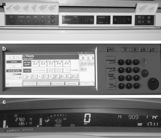
Figure 8.1 The human interface in some familiar products. (a) Domestic fridge. (b) Photocopier. (c) Car dashboard (detail)
The photocopier control is somewhat more complex. There is a wide range of operating modes available, with different paper sources and image adjustment capabilities available. Information is conveyed by a customised display. As this is touch-sensitive, it also acts as an input of control information. A more conventional numerical keypad allows input of purely numerical data, such as codes and the number of copies required.
The detail from the car dashboard represents a further increase in complexity. Its central feature is car speed – as the car in this instance is stationary this shows a big zero. Around this, one can see a range of status information, including things as diverse as engine r.p.m., radio station, temperature, door status and fuel. Despite the complexity and diversity of information, it is all conveyed in simple forms. Again, there is considerable use of numerical display. To this are added bar graphs, simple illuminated symbols and simple diagrammatic information. No user input is seen in this picture.
What is striking in each of these three very diverse interfaces is the strands which unite them. Each has significant need to convey numerical information and status information; means are found to achieve both of these in simple ways. The main sense invoked is sight. Sound is also used, especially in alarm situations.
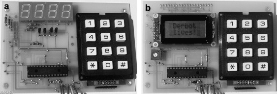
We will be exploring means of information exchange between the embedded system and user in the section that follows. This will be done through a study of the keypad, seven-segment LED (light-emitting diode) display and the liquid crystal display (LCD), as these are more or less ubiquitous in simple embedded systems. These will be illustrated with the Derbot ‘hand controller’ module. This is an optional unit that can be hand-held or fitted above the battery pack, as seen in Figure A3.3. The hand controller is available in two versions, one for an LED display and one for an LCD. These are shown in Figure 8.2. The hand controller is designed as a ‘dumb terminal’ which interfaces directly with the main Derbot AGV. It can, however, be used in stand-alone form, which is the case in this chapter. In Chapter 10 it is linked to the AGV and used to illustrate serial communications. Its circuit diagram is given in Figure A3.2.
8.2 From switches to keypads
The humble switch, mainstay of so many human interfaces, was introduced in Chapter 3. Switches are good for conveying information of a digital nature – they are two-state, but can be used in multiples, each one taking one port bit. In more complex situations it becomes inappropriate to keep adding switches. For one thing, the demand on port bits becomes excessive, and their relentlessly two-state nature often does not meet the need.
8.2.1 The keypad
A useful step forward from the simple switch is given by the keypad, as seen in the photocopier interface and the Derbot hand controllers in Figure 8.2. The keypad allows numeric or alphanumeric information to be entered. It is widely used in photocopiers, burglar alarms, central heating controllers and so on.
A keypad is based on switches, yet it would be extremely resource-intensive if each of these switches were allocated to a port bit. Instead, to make good use of resources, each switch is connected in a matrix. Figure 8.3 shows the electrical connections for the keypad of Figure 8.2, which has 12 keys. It can be seen that these are arranged in a 4 × 3 matrix, with four rows and three columns. Now only seven interconnections are needed, rather than 12. Whenever a key is pressed, it connects its row with its column.
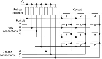
In an embedded environment the keypad is usually connected to the bits of a microcontroller input/output (I/O) port. Example port bit connections are shown in the figure, as well as the necessary pull-up resistors. The challenge is how to detect efficiently which key has been pressed.
The technique usually used to read a keypad follows the flow diagram of Figure 8.4(a). First the column bits are set to output, with the row bits as input. The output column bits are set to 0. If no button is pressed all row line inputs will read 1, due to the action of the pull-up resistors. If, however, a button is pressed then its corresponding switch will connect column and row lines, and the corresponding row line will be pulled low. If the same process is repeated instantaneously, but with outputs exchanged for inputs, then the column line for the key pressed can be found and the key fully identified.
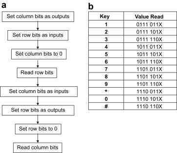
Figure 8.4 Reading a keypad with a microcontroller port. (a) Flow diagram. (b) Outputs for keypad of Figure 8.3
Output values for the keypad connection shown in Figure 8.3 are shown in Figure 8.4(b). For example, suppose key 7 was pressed. In the first phase of the flow diagram, with row connections as inputs, the third row line (port bit 5) would read low. In the second phase, with column bits as inputs, the first column (port bit 3) would read low. The final pattern is as shown, with bit 0 showing a ‘don't care’ condition, as it is unused.
8.2.2 Design example: use of a keypad in the Derbot hand controller
The flow diagram just described is only the starting point for working with keypads. How, for example, do we detect when the keypad is actually pressed and what do we do with the code appearing in the table?
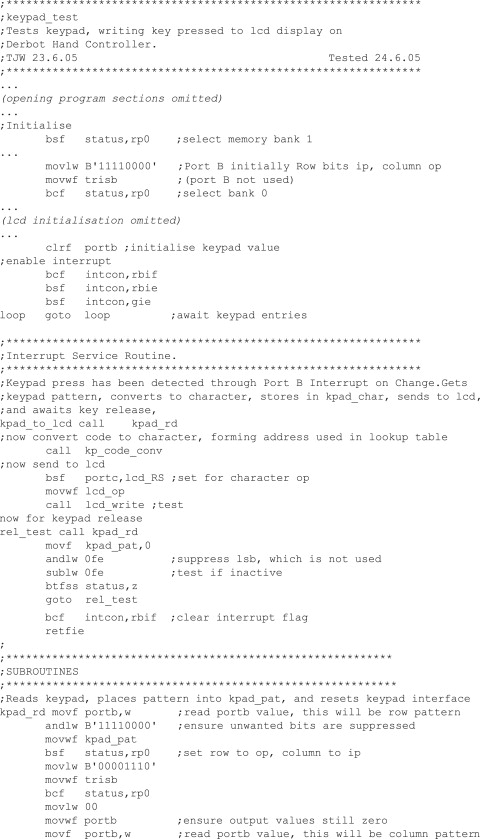
Program Example 8.1 illustrates a practical application of keypad reading in a program called keypad_test. The program is used to illustrate use of both keypad and LCD. It is too long to print in its entirety, so the keypad-related sections only are reproduced here. The book’s companion website contains the full program.
The program flow diagram is shown in Figure 8.5. To detect keypad action, it uses the ‘interrupt on change’ facility, available on the higher four bits of Port B. Following initialisation, all program activity is contained in the Interrupt Service Routine, called kpad_to_lcd. This does essentially four things. It reads a pattern from the keypad, converts this to ASCII code, sends the code to the LCD and waits for the key to be released, before leaving the ISR.
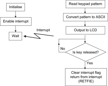
Try following the program through, matching it with the flow diagrams shown. In the opening initialisation Port B is set up so that row bits are input and column bits are output. We could start the other way round, but to make use of the ‘interrupt on change’, the higher four bits must be set as input. All output bits are subsequently set to zero and the ‘interrupt on change’ interrupt is enabled. We have at this stage already entered the flow diagram of Figure 8.4(a).
An interrupt occurs when a key is pressed and the Interrupt Service Routine, labelled kpad_to_lcd, is invoked. This immediately calls the subroutine kpad_rd, which continues the flow diagram of Figure 8.4(a), started in the initialisation section. The value of Port B is read and stored in memory location kpad_pat. Column and row roles are then reversed, and the row bits are then read. These are ORed into kpad_pat, ensuring that any unwanted bits are removed by ANDing with 0. The routine then resets Port B to its initial value, ready for the next keypad read.
The value held in kpad_pat, on completing the kpad_rd subroutine, is not in a very useful format. It is a 7-bit number, with possible values shown in Figure 8.4(b). The program therefore calls subroutine kp_code_conv, which converts this number into the keypad code that caused it. The way this is done is described in the next paragraph. This value is then output to the LCD, using subroutine lcd_write. This is not shown in this example, but is described later in the chapter. The program then sits in a loop, waiting for release of the key, invoking the kpad_rd subroutine again. This is because the user letting go of the keypad will also cause an ‘interrupt on change’, which would lead to a second, unwanted keypad read.
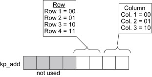
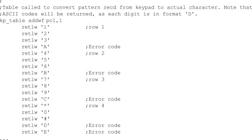
The kp_code_conv subroutine converts the patterns derived from reading the keypad, as seen in Figure 8.4(b), into the ASCII code of the key pressed. It does this by deriving an address, held in memory location kpad_add, which is used to access the look-up table kp_table. The address follows the format shown in Figure 8.6. The subroutine tests the bits of the pattern in turn, finding out which row and column has been active. It sets up the address bits according to the outcome of its tests. The look-up table is then called, as described in Chapter 5.
8.3 LED displays
The first part of this chapter showed how very important displays are, in almost any system which has a human interface. We look at two types of display here, the seven-segment LED and the liquid crystal.
8.3.1 LED arrays: seven-segment displays
Along with the switch, the simple LED was introduced in Chapter 3. We saw that LEDs are visually attractive, are an efficient source of light, can be driven from a logic gate or port bit output and are thus exceptionally useful for conveying simple information. Yet the single LED, or even groups of LEDs, are restricted in the information they can give, and as their number increases they become increasingly complex to drive. There are therefore a number of standard configurations in which LEDs are packaged, including bar-graph, seven-segment display, dot matrix and ‘star-burst’.
The seven-segment display is a particularly versatile configuration, seen already in Figures 8.1(a, c) and 8.2(a). We explore the LED implementation of it in some more detail here. A single digit, made by Kingbright [Ref. 8.1], is shown in Figure 8.7. This is the display used in the Derbot hand controller (Figure 8.2(a)). By lighting different combinations of the seven segments, all numerical digits can be displayed, as well as a surprising number of alphabetic characters. A decimal point is usually included, as shown. The problem arises that if each segment is illuminated by an LED, then 14 connections are required, and that is just for one digit. If multiple digits are required, then the number of connections soars. Therefore, two clever and simple techniques are used to tame the number of connections used.
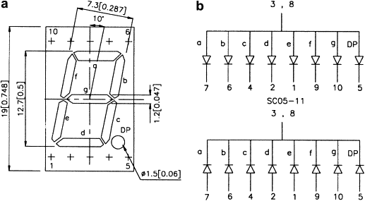
Figure 8.7 The seven-segment display. (a) A seven-segment digit (Kingbright, 12.7 mm). (b) Electrical connection (upper: common anode; lower: common cathode).
Reproduced with permission of Kingbright Elec. Co. Ltd
The common anode/common cathode connection
When using multiple LEDs in simple configurations, it is almost certain that one ‘side’ of all the LED terminals will be connected to all others of the same type. In other words, all LED anodes are likely to be connected together, or all LED cathodes. This is what is done in the seven-segment digit, as seen in Figure 8.7(b). The digit is available either in common cathode or common anode form. There are eight LEDs in the digit (including the decimal point), but instead of 16 connections being needed, there are now only nine, one for each segment and one for the common connection. The actual pin connections in the example shown lie in two rows, at the top and bottom of the digit. There are 10 pins in all, with the common anode or cathode taking two pins.
Multiplexing of digits
By making a common cathode or common anode connection, the number of connections to a single digit is reduced. But a digit on its own is rarely used and multiple digits will still require many connections. A four-digit display, for example, with decimal points on each digit, would require 36 connections. Furthermore, a multi-digit display would have power supply requirements that are quite excessive. With all segments on, and each taking 5 mA, it would draw 160 mA. Therefore, a second, important technique is introduced, that of digit ‘multiplexing’. While this enables us to develop a practical display, it also poses an interesting early challenge in handling some real-time issues. The technique is illustrated in the design example that follows.
8.3.2 Design example: the Derbot hand controller seven-segment display
The circuit diagram of the Derbot hand controller in Figure A3.2 is comparatively complex, as the controller can be used in the LED version or LCD version (but not both). The seven-segment LED display section alone is shown in Figure 8.8(a), and from this an understanding of digit multiplexing can be developed. It can be seen that all equivalent segment lines are connected together, so that, for example, segment ‘a’ of Digit 1 is connected to segment ‘a’ of Digit 2 and so on. Each of these segment lines is connected via a resistor (1.2 kΩ; not shown) to a port bit. Kingbright ‘high-efficiency red’ common cathode displays are used [Ref. 8.1].
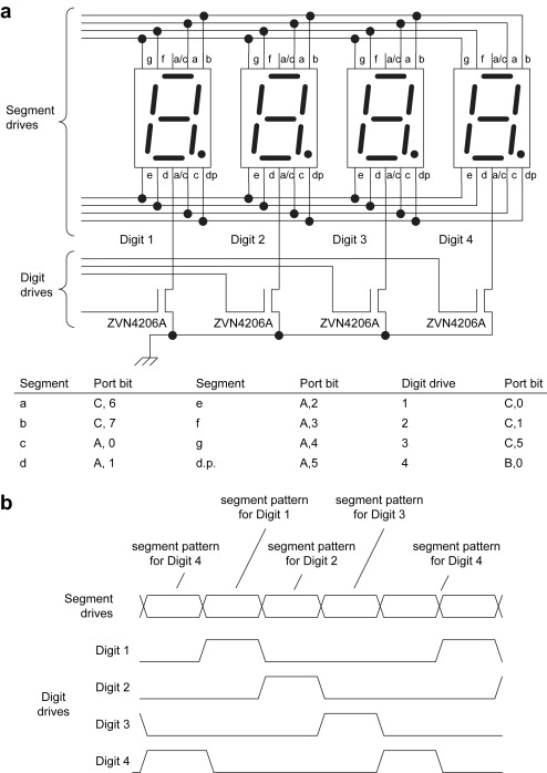
Figure 8.8 Seven-segment display part of the Derbot ‘hand controller’. (a) Detail of display circuit diagram. (b) Timing diagram for driving the digits
Each of the digit common cathode lines is connected to a ‘logic-compatible’ MOSFET transistor. When the gate voltage of the transistor goes high, the transistor conducts and the common cathode terminal goes low. (Further details on transistor switching are given later in the chapter.) Any segment whose anode is at logic high then illuminates. The value of the series resistors is selected experimentally to minimise the current while maintaining reasonable visibility. Noting from the data that each LED has a forward voltage when in conduction of around 1.9 V, the current I flowing per segment can be calculated as:
This calculation neglects the ‘on’ resistance of the switching transistor and the output resistance of the port. Both of these are small compared with the 1.2 kΩ value of the series resistance.
The way this display is driven is shown in the timing diagram (Figure 8.8(b)). The digits are activated continuously in turn. If this is done at the right speed, the eye is tricked into thinking that all digits are being continuously lit. The timing diagram shows the segments for Digit 4 being set and the Digit 4 common cathode being set to 1. Digit 4 is therefore switched on, while all other digits are off. This is held for a time (around 5–20 ms is generally appropriate) and then Digit 2 is illuminated in a similar way. Each digit is lit in turn and the cycle recommences.
If driven from a microcontroller, a program must be written to recreate the timing diagram. Let us see how this is done in practice, in Program Example 8.2. This is a very simple program, which runs on the LED version of the hand controller, and does nothing but display the word HELP on the digits. Figure 8.7(a) shows that, for the letter H, segments b, c, e, f and g should be illuminated. After a simple initialisation, the bit pattern for the letter H is set up on Ports A and C, by setting high each of the bits connected to the ‘on’ segments. The common cathode of Digit 1 is also set high and a 5 ms delay called. The H segments, and the Digit 1 common cathode drive, are then replaced by the segments for the letter E and the common cathode drive for Digit 2. The program continues through all four letters, before looping back to start again.
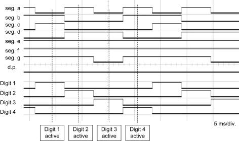
Figure 8.9 shows a screen print from the logic analyser section of the Agilent Mixed Signal Oscilloscope, with the program running. All segment lines are shown, together with the four digit drives. When any digit common cathode drive is high, the associated common cathode connection itself is taken low and the digit is activated. For Digit 1, it is easy to see the segments b, c, e, f and g are on, forming the letter H. Similarly, for Digit 2, the segments a, d, e, f and g form the letter E, and so on. The process repeats continuously and the word HELP is spelt out. It can be seen that segments e and f are continuously on, while the decimal point (d.p.) is always off.
Light-emitting diodes are enormously useful, but they suffer from several drawbacks: they are power-hungry, at least for battery-powered designs, and it is difficult, if not impossible, to form them into complex multi-digit or graphical displays. Therefore, it is essential to look elsewhere for sophisticated displays, with the solution being readily found in liquid crystal technology.
8.4 Liquid crystal displays
The liquid crystal display (LCD) has been one of the enabling technologies of the current electronic revolution. It is an essential part of every mobile phone, every laptop and every personal organiser.
Liquid crystal is an organic compound that polarises any light that passes through it. Liquid crystal also responds to an applied electric field by changing the alignment of its molecules, and in so doing changing the direction of the light polarisation that it introduces. Liquid crystal can be trapped between two parallel sheets of glass, with a matching pattern of transparent electrode on each sheet. When a voltage is applied to the electrodes, the optical character of the crystal changes and the electrode pattern appears in the crystal.
A huge range of LCDs has been developed, including those based on seven-segment digits or dot matrix formats, as well as a variety of graphical forms. Many general-purpose displays are available commercially, while customised displays are made for large-volume products. The Derbot hand controller uses an example of a very popular and useful general-purpose format, as seen in Figure 8.2(b). The display shown has two lines, of eight digits each, where each digit is a liquid crystal dot matrix. Larger displays in this format are common, with more digits and more lines.
Driving LCDs directly is not entirely simple. That need not concern us too much here, however, as most displays, like the one shown in Figure 8.2(b), contain their own drive electronics, designed to be interfaced to a microcontroller. The need is then to understand how to interface to the drive electronics.
8.4.1 The HD44780 LCD driver and its derivatives
Some few years back the electronics giant Hitachi developed a microcontroller specially designed to drive LCD alphanumeric modules such as the one shown in Figure 8.2(b). In turn, it had a simple interface that could be connected to general-purpose microprocessors and microcontrollers. This microcontroller, the HD44780 [Ref. 8.2], defined an interface that has become something of an informal standard for this type of display. Many manufacturers of displays integrated it into their products. A generation of derivatives now exists which has replaced the original Hitachi device but retained most of its features. These include the S6A009 and KS0066U devices made by Samsung. As these derivatives tend to be so similar to the original Hitachi device, the HD44780 features will be described. When designing with a display it is important, however, to ensure that you are working with the correct data for the device.
The HD44780 interface has some peculiarities, partly due to the time-scale laid down by the display itself. It has the following highlights:
• Data is transferred on a 4- or 8-bit data bus, determined by the user. Data may be instruction or character information. Using the 4-bit mode allows the whole interface to be contained within just seven bits, but the data transfer process is a little slower. Bit 7 of the data bus doubles as a ‘busy flag’, indicating whether the device is ready to accept new data. This is very important, as many operations of the HD44780 take finite time and must be completed before another instruction can be accepted.
• There is a simple instruction set which allows control of operating characteristics – this includes initialising and clearing the display, and controlling the position and characteristics of the cursor.
• The user can access two registers, depending on the state of the RS line:
• Internal resources include 80 bytes of display RAM and a character generator ROM.
On power-up, the HD44780 must undergo a very specific initialisation process. It is important to get this absolutely right, or any HD44780-driven display may just sit inactive. An instruction sequence is given in the data accompanying any commercially available display based on this interface. An example is reproduced in Ref. 8.3. The early initialisation instructions are independent of whether the display is in 4- or 8-bit mode and the busy flag is not initially available. Therefore, these initialisation instructions are usually separated by delay routines of appropriate duration, to ensure that one action is completed before the next is started.
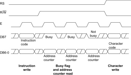
The HD44780, constrained as it is by the timing requirements of the LCD itself, tends to operate at a slower speed than most microcontrollers. Interfacing with it therefore carries some unique timing problems. An example timing diagram, for an 8-bit interface, is shown in Figure 8.10. Every data transfer to the LCD controller is made by a pulse on the E line. With RS initially set low, the data placed by the microcontroller on the data bus is interpreted as an instruction, which the HD44780 receives and starts to execute. The microcontroller needs to know when that instruction has been completed. ![]() is therefore taken high, so on the next cycle of E the LCD controller outputs to the data bus a word made of the busy flag as MSB, with lower bits made up of the internal RAM address counter. No further data can be sent to the LCD controller until the busy flag is cleared, so it is checked repeatedly. When it goes low, RS in this example is taken high,
is therefore taken high, so on the next cycle of E the LCD controller outputs to the data bus a word made of the busy flag as MSB, with lower bits made up of the internal RAM address counter. No further data can be sent to the LCD controller until the busy flag is cleared, so it is checked repeatedly. When it goes low, RS in this example is taken high, ![]() is taken low and the next data transfer is therefore a character code.
is taken low and the next data transfer is therefore a character code.
8.4.2 Design example: use of LCD display in the Derbot hand controller
The Derbot hand controller, in its LCD version, uses a Powertip PC0802-A display [Ref. 8.4]. This display has two lines, each of eight characters. It is controlled by the S6A0069 LCD driver microcontroller, which has the features of the HD44780 just described. It is used in 8-bit interface mode. The full circuit diagram is given in Figure A3.2, with the LCD-only detail given in Figure 8.11.
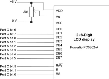
Figure 8.11 Connections to the Powertip PC0802 LCD display, showing connections for the Derbot hand controller
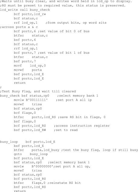
The program used to demonstrate the LCD display is keypad_test, which has already been quoted in Program Example 8.1. When a keypad key is pressed, this program identifies it and transfers the key number, in ASCII, to the LCD. The subroutines to write an instruction or character code to the display controller, lcd_write, and to check the busy flag, busy_check, are shown in Program Example 8.3. The initialisation process can be seen by checking the full program listing on the book’s companion website.
The lcd_write subroutine starts with a call to the busy_check subroutine, so that no attempt is made to write to the display controller unless it is ready to receive. The subroutine then sets the ![]() line low, to indicate a write process is about to occur. The subroutine is rendered a little more complex as the hardware design splits the 8-bit bus to the LCD controller across two ports (Figure 8.11), so two shifts right must be undertaken. Once the correct data value is set up on the port, the enable line, labelled lcd_E, is pulsed high to complete the transfer.
line low, to indicate a write process is about to occur. The subroutine is rendered a little more complex as the hardware design splits the 8-bit bus to the LCD controller across two ports (Figure 8.11), so two shifts right must be undertaken. Once the correct data value is set up on the port, the enable line, labelled lcd_E, is pulsed high to complete the transfer.
The busy_check routine first sets Port A to input. The value of RS, which can be in either logic state, is saved. This line is then set low, and ![]() set high, which sets the condition for a read of the busy flag. The E line is then strobed high and a test of the busy flag occurs. The subroutine loops until the busy flag is cleared.
set high, which sets the condition for a read of the busy flag. The E line is then strobed high and a test of the busy flag occurs. The subroutine loops until the busy flag is cleared.
Liquid crystal displays such as the one just described are enormously useful in the world of small to medium embedded systems. They are low-power and comparatively flexible in their use. On the downside, interfacing to them can be tiresome, with not insignificant blocks of code required just to transfer simple messages. Because their interface is slow, they can become a limiting factor in high-speed systems.
8.5 The main idea – interfacing to the physical world
Whether or not the embedded microcontroller has a human interface, it will certainly interface with the physical world. To do this it must be able to detect the state of physical variables and it must be able to control those variables. This interaction with the physical world is done by
means of transducers, a major field of study in themselves. ‘Input transducers’, also called sensors, detect and convert physical variables into electrical variables. Examples include light or temperature sensors, or sensors which detect physical position, including measurement of distance or rotary displacement. Output transducers convert electrical variables to physical. Ones which cause physical movement, our main interest here, are also called actuators. Examples include solenoids and motors.
In our study of embedded systems, we need knowledge of what transducers are available, what they can do and how we can interface to them. In the remaining part of this chapter, therefore, some interfacing techniques essential to embedded systems are introduced. The transducers used in the Derbot AGV are also introduced. While this might seem an arbitrary choice, they are as good a selection as any – it would be impossible in this book to attempt to undertake a comprehensive survey of all transducers.
8.6 Some simple sensors
There is an enormous range of sensors available today, some with a long history and others based on very recent technology. These include ‘smart’ or ‘intelligent’ sensors, which are integrated onto an IC and have on-chip signal processing. All are based on one or an other physical phenomenon that leads to the conversion of physical variables to electrical, sometimes via an intermediate variable. The sensors introduced here include electromechanical, optical and ultrasonic. Some are shown in Figure 8.12.
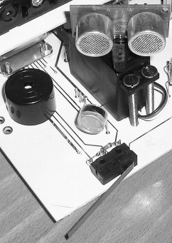
Figure 8.12 Some of the Derbot's sensors and actuators – an ultrasonic distance sensor mounted on a Futaba servo, behind a light-dependent resistor and microswitch
8.6.1 The microswitch
The microswitch has been the mainstay of mechanical position sensing over many years, and is likely to retain that position in years to come. Usually, it is in the form of a single-pole, double-throw switch, with a lever or roller for actuation. Microswitches are available from the sub-miniature to the large and rugged, for heavy-duty industrial applications. Electrically they can be interfaced just like a normal toggle switch, using one of the circuits shown in Figure 3.7. In industrial applications further precautions may be taken to minimise electrical interference. On the Derbot two microswitches are used as ‘bump’ sensors, one of which is seen in Figure 8.12.
8.6.2 Light-dependent resistors
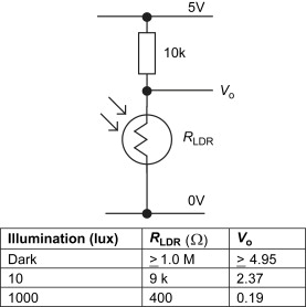
A light-dependent resistor (LDR) is made from a piece of exposed semiconductor material. When light falls on it, it creates hole-electron pairs in the material, which improve the conductivity. When light is removed, the hole-electron pairs recombine and conductivity falls. The overall effect is that as illumination increases, the LDR resistance falls.
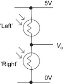
The LDR used in the Derbot is the NORP12, made by Silonex [Ref. 8.5], with a resistance when completely dark of at least 1.0 MΩ, falling to a few hundred ohms when very brightly illuminated. It can be connected in a simple potential divider to give a voltage output, as shown in Figure 8.13. The Derbot has three of these sensors, which it uses when in light-seeking mode. These can be seen in Figure A3.1. They are connected to the 16F873A analog-to-digital converter inputs described in Chapter 11.
8.6.3 Optical object sensing
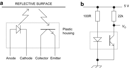
Optical methods are very useful in sensing objects and surfaces. In one configuration the presence of an object can be sensed if it breaks a light beam, in another if it reflects the beam. Many sensors are available with both light source and sensor integrated into the same package. The Derbot AGV uses reflective opto-sensors made by Optek, type OPB608A [Ref. 8.6].
The principle of this sensor is illustrated in Figure 8.14(a). The sensor consists of an infrared LED and phototransistor mounted side by side in the same plastic package. The package material allows infrared light to pass, but filters ambient visible light. When a reflective surface is placed at a suitable distance in front of the sensor, some of the emitted light is reflected back to the phototransistor, which then conducts. If the sensor is connected in the circuit of Figure 8.14(b), then the circuit output VO is at Logic 1 when no reflection occurs and goes to Logic 0 if a reflective surface is present. Resistor values are dependent on sensor characteristics, the ones given here being indicative. The distance from sensor to reflective surface is critical in many such sensors, with preferred distances around 3 mm being common.
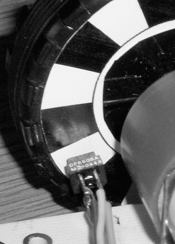
8.6.4 The opto-sensor applied as a shaft encoder
In the Derbot, the reflective opto-sensors just described are used to create very simple shaft encoders, as can be seen in Figure 8.15. A card with a simple black/white pattern (Figure A3.4) is fixed to the wheel, with the sensor face positioned around 3 mm away from it. As the wheel rotates, the sensor produces an approximate square wave, with logic high every time a black section of the pattern goes by. (An actual waveform is shown in Figure 8.20, where the conditioning requirements of the signal are investigated.) If these pulses are counted, they can be used as the basis for distance measurement, or odometry, in the AGV. This is developed further in later chapters. It should be mentioned that the handmade shaft encoder developed here is very crude compared to commercially available units. Whereas the Derbot shaft encoder generates 16 pulses per revolution, a commercial unit can generate hundreds of cycles, giving a far improved resolution.
8.6.5 Ultrasonic object sensor
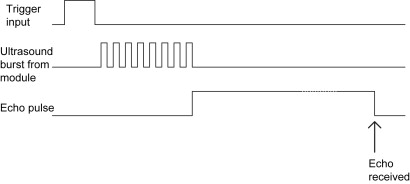
Ultrasound is widely used for sensing and measurement, from simple distance measurement to complex medical imaging. The Derbot AGV uses an ultrasonic reflective sensor to detect obstacles in its path or to allow it to run parallel to a wall. The sensor, a Devantech SRF04 [Ref. 8.7], is seen in Figure 8.12. A SRF05 has very similar performance, and can also be used.
The sensor consists of a transmitter and receiver and, to the extent that it is based on a reflective principle, is initially similar to the reflective opto-sensor. The big difference lies in the fact that the ultrasound source is pulsed and the time taken for the echo to return is measured; from this a distance can be calculated. The timing diagram of the sensor is shown in Figure 8.16. A logic pulse is input to the module trigger input. This causes an eight-cycle ultrasonic burst to be generated. The echo output of the module then goes high and remains high until an echo is detected, at which point it goes low. If the duration of the pulse is measured, then the distance of the object that caused the reflection can be calculated.
8.7 More on digital input
If a microcontroller is to receive logic signals, then it is essential that those signals are at voltage levels which are recognised by it as being either Logic 0 or Logic 1. These voltage levels are usually defined by a logic family, for example TTL (Transistor Transistor Logic) or CMOS (Complementary Metal Oxide Semiconductor). When one device is connected to another, and each is supplied by the same voltage and is of the same logic family, then it is usually safe to assume that logic levels will be safely and reliably transferred. However, if signals are generated from a non-logic source, e.g. a sensor, or if they have been received over a long communication link, or have been subject to interference, then it may be that they are not correctly interpreted by the receiver.
8.7.1 16F873A input characteristics
To determine whether a signal will be properly received by a logic device, it is first necessary to understand its input characteristics. The characteristics for a 16F873A port bit, taken from Ref. 7.1, are shown diagrammatically in Figure 8.17. From this it can be seen that any input voltage lying between 0 and 0.8 V is interpreted as a Logic 0, and any lying between 2 and 5 V is interpreted as a Logic 1. An input voltage lying between these two regions is not defined.
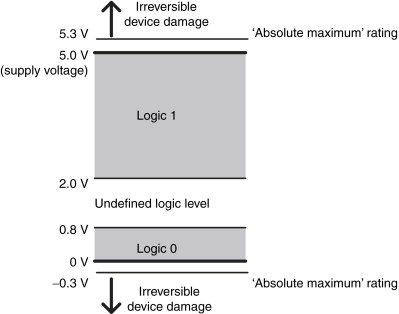
If the input voltage exceeds 5 V, then there is a danger of damage to the device. Logic inputs, however, almost invariably have internal protection diodes, one connected from input to ground, the other from input to supply rail. This arrangement can be seen by looking forward to Figure 8.19(a). Both diodes are connected so that in normal operation they are reverse-biased. However, if the input voltage exceeds the supply rail by a voltage adequate to cause diode conduction, then the diode connected between them will start to conduct and the input voltage will be clamped at that voltage. Similarly, if the input falls sufficiently below 0 V, then the other diode will start to conduct. This mechanism offers some protection to the input circuit.
For the 16F873A, input protection diodes come into action at +5.3 or −0.3 V. These do not, however, have limitless capability; the maximum input clamp current is specified as ±20 mA. If the absolute maximum voltages are significantly exceeded, then damage will occur, probably starting with the destruction of a protection diode.
8.7.2 Ensuring legal logic levels and input protection
It is up to the designer to ensure that the input voltage is only ever steady-state in one of the recognised logic levels, i.e. one of the shaded zones of Figure 8.17. It can pass quickly through the intermediate undefined zone, but must not linger there. It must never exceed the maximum ratings. It will meet these conditions if signals are generated locally, by another logic device of the same family. If, however, the signal has been transmitted over a long distance, maybe from a remote sensor, if there is interference, or if it was never a proper logic signal in the first place, then problems may arise.
Figure 8.18 shows sketches of a number of forms that a corrupted signal can take. Signal (a) has acquired positive-going spikes, which are potentially damaging to the input circuit. Signal (b) has similarly acquired voltage spikes. While these are not at a level that will damage the input circuit, they may well lead to misleading results, particularly if the signal is to be input to a counter, or is a serial clock or data signal. Signal (c) has very slow edges, perhaps due to the filtering effect of a long cable or because the source is from a sensor. Finally, signal (d) looks like a reasonably healthy logic signal, but it has picked up a voltage offset. This could be due to long-distance transmission, with a voltage differential between the earth references at transmitter and receiver.
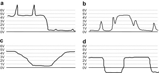
Figure 8.18 Different forms of signal corruption. (a) Spikes in signal, potentially harmful to device input. (b) Spikes in signal. (c) Excessively slow edges. (d) DC offset in signal
A variety of techniques are available to try to correct problems like these and to ensure legal logic levels. These are found in any good electronics textbook. Figure 8.19 illustrates three of them.
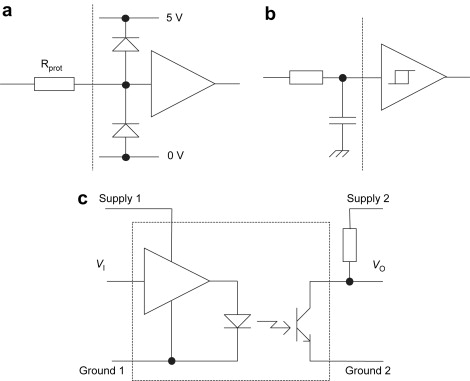
Figure 8.19 Some simple methods to condition a digital input. (a) Invoking protection diodes. (b) Filtering spikes with Schmitt trigger. (c) Isolation or level shifting with the opto-isolator
Clamping voltage spikes – with current-limiting resistor
It has been mentioned that, if too much current flows in the protection diodes, they will themselves burn out. Therefore, if there is a chance of the protection diodes being invoked, then it is worth including a series resistor to limit the current that may flow in them. This is shown in Figure 8.19(a). Such a method would correct the corrupted signal of Figure 8.18(a) if the magnitude of the spikes was not too great.
Suppose in Figure 8.19(a) that the maximum permissible diode current was 20 mA, Rprot was 1 kΩ and the upper protection diode started to conduct when the input voltage was 5.3 V. Then the maximum permissible voltage spike would have a peak value of [(20 mA × 1 kΩ) + 5.3], or around 25 V.
Schmitt trigger
The Schmitt trigger was described in Chapter 3. It provides an easy means of speeding up slow logic edges, such as are seen in Figure 8.18(c).
Analog input filtering
Sometimes a logic signal picks up interference that is not potentially damaging to the microcontroller but can cause problems in the system operation. For example, if the signal is the input to a counter, then spurious counts will occur if there are voltage spikes in the signal. A simple RC filter, as seen in Figure 8.19(b), is sometimes enough to remove low-level interference. The edges of the signal, which will have been slowed by the filter, can be recovered by means of the Schmitt trigger. This approach could solve the problem seen in the signal of Figure 8.18(b).
Figure 8.20 shows the oscilloscope trace at the output of one of the reflective opto-sensors on the Derbot AGV. The connections to this run close to the motors, which being brushed DC motors are a rich source of interference. The signals are connected to the inputs of Timer 0 and Timer 1. While the signal does not look severely corrupted, it was found that the little voltage spikes that are present are quite enough to introduce spurious counts.
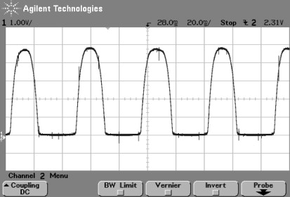
As the circuit diagram of Figure A3.1 shows, an RC filter having component values R = 11 kΩ, C = 10 nF (i.e. cut-off frequency close to 1.4 kHz) is inserted in the signal path. This is well above the maximum frequency of 40 Hz expected from the shaft encoder, but proved adequate to remove the effects of the voltage spikes. The Schmitt trigger inputs of both timers then serve to correct the slow rate of change of the incoming signal.
Opto-isolation
The opto-isolator, as seen in Figure 8.19(c), is a very useful means of protecting a logic input, especially when a signal has been received over a distance. The incoming signal drives an LED, whose light output activates an opto-transistor. There is no electrical connection between input and output, so problems such as the earth differential, seen in Figure 8.18(d), can be resolved.
Digital input filtering
Many ICs designed to accept signals that may carry interference have some form of digital input filtering designed into their input circuits. This is the case with the 16F873A, as we shall see in Chapter 10 with the asynchronous serial input. A simple digital filtering strategy is to sample the input three times in succession and then use a ‘majority vote’ circuit to determine the logic value to be accepted. Thus, if two ones and one zero are detected, the Logic 1 will be accepted and the zero – possibly representing a glitch due to interference – discarded. The sampling must of course occur at a faster rate than any intended rate of genuine input change.
8.7.3 Switch debouncing
A particular problem with mechanical switches is the property that the switch contacts literally bounce as they close. This leads to a short period, generally less than 10 ms, when the switch state bounces between open and closed. When switching on a conventional electrical load, like a light, this is not a problem and is not even noticed. When connected to a digital circuit, particularly one that has a rapid response or is counting, the effect can be disastrous.
A number of standard methods exist to eliminate the effect of switch bounce. Hardware techniques, generally based on bistables or Schmitt triggers, can be found in any good electronics textbook and in Ref. 1.1. It is interesting to explore software techniques briefly here, as these can be implemented in a system without extra cost. Figure 8.21 shows two possibilities. In (a) and (b), a switched input is being polled (i.e. read periodically), with the polling period being greater than the period of switch bounce. If, as in (a), the switch change and bounce occurs between input polls, then a clean transition is perceived. If the input is polled as the switch bounce occurs, as in (b), then the logic value read is unpredictable. Either the previous logic state is detected and retained for another poll interval (dotted line) or the new logic state is detected (solid line), a value repeated at the next poll. In either case the transition is clean.
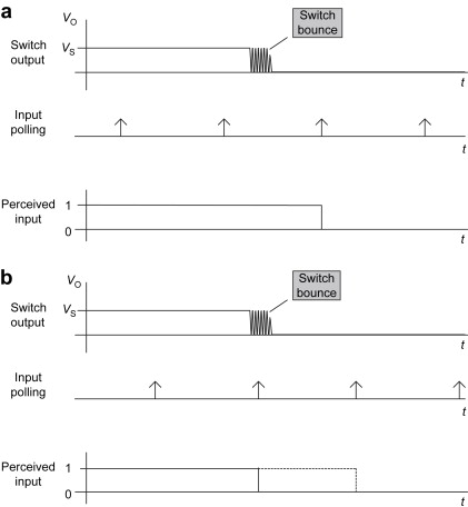
Figure 8.21 Eliminating switch bounce by polling. (a) Input poll misses bounce. (b) Input poll hits bounce
Sometimes the programmer does not want to poll an input, but may instead use it to force an interrupt. If the interrupt is caused by a single switch changing to a known state (for example, always switching from high to low), then switch bounce is unlikely to cause a problem. The interrupt could, however, be caused by one of several switches, for example the keypad read described earlier in this chapter. If the switch states were read immediately the interrupt occurred, then the read would probably occur during the period of switch bounce. In this case a short programmed delay, following the first detection of change, can be introduced. Switch states can then be read at the end of the delay, when the bounce has completed.
8.8 Actuators: motors and servos
A common requirement in an embedded system is to cause physical movement. This is usually either linear, i.e. movement in a straight line, or rotary. Many of the actuators used to create these movements are electrical. Solenoids can be used for linear movement, ‘servos’ for angular only, and DC or stepper motors for angular or rotary. Other actuation methods, particularly for high forces, include pneumatic and hydraulic.
8.8.1 DC and stepper motors
DC and stepper motors are very widely used in embedded systems. While based on very different operating principles, they tend to compete for similar applications. Given the right operating environment, both can be used for continuous rotary motion or for precise angular displacement.
DC motors range from the extremely powerful to the very small. DC motors drive huge electric trains but also tiny mechatronic systems. Their popularity is due to their wide, useful speed range, the ability to control this speed and their potentially good efficiency. When used with a feedback potentiometer or shaft encoder, they can be used to provide accurate angular positioning. Small DC motors, such as are used in embedded systems, are usually of the permanent magnet type, i.e. the magnetic field within which the armature rotates is provided by one or more permanent magnets. This leads to one of the attractive features of the DC motor – its operating simplicity. Only the armature winding needs to be driven.
The big attraction of stepper motors is their ability to interface very directly with a digital system. Each digital pulse sent to a stepper controller can be used to advance the motor shaft position by a known angle. Therefore, in theory, a microprocessor or microcontrollers can control speed and angular position of the motor shaft to a high level of accuracy, without feedback. In practice this happy position is not completely achieved. Stepper motors have awkward start-up characteristics, show mechanical resonance in a particular speed range and lose torque at high speed, with a limited top speed. Any of these factors can cause the motor to lose synchronisation with its digital drive. On top of this, stepper motors tend to be less efficient and more complex to drive than DC motors.
The choice between stepper and DC motors is not always an obvious one. In general, if precise and limited rotary motion is required, and power consumption is not of primary importance, then stepper motors usually win. If less precision is needed, and perhaps higher speed and/or higher efficiency, then a DC motor may be the choice.
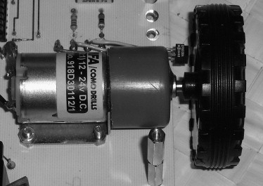
The Derbot AGV needs controllable rotary actuation to drive its wheels. It steers by these, and needs to exercise speed and distance control. All these functions could be achieved by stepper motors. However, the simplicity of driving DC motors, coupled with their good efficiency – essential for the Derbot battery operation – led to the choice of this type of motor. To effect control some form of feedback was necessary. For this the simple shaft encoder already described was implemented. The version of the Derbot described in this book uses a geared motor made by MFA/Como Drills [Ref. 8.8]. The motor is pictured in Figure 8.22, with basic data provided in Tables A3.1 and A3.2.
8.8.2 Angular positioning: the ‘servo’
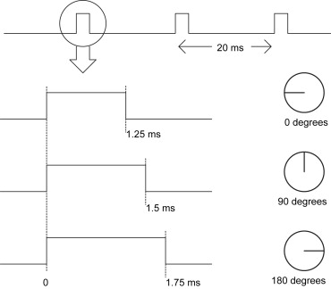
The ‘servo’ is a device that has claimed the generic title of servomechanism for its own! Widely used in radio-controlled modelling and robotics, it allows precise angular positioning. The servo output is a shaft that can take an angular position over a range of around 180°. The input to the servo is a pulse stream, generally of repetition rate 50 Hz (i.e. period of 20 ms). The ‘width’ of the input pulse determines the angular position of the output shaft. In the example of Figure 8.23, a pulse width of 1.25 ms leads to an output shaft position of 0°, 1.5 ms to an output shaft position of 90° and 1.75 ms to an output shaft position of 180°. This is an example of pulse width modulation, which we shall meet in later chapters.
In some of its configurations the Derbot uses the Futaba S3003 servo [Ref. 8.9] to rotate the ultrasonic sensor, thus allowing a single sensor to make measurements in different directions. The servo draws significant current as it turns, and for this reason it is helpful to add a larger capacitor across the supply lines to help maintain the supply voltage. See the book website for more details.
8.9 Interfacing to actuators
8.9.1 Simple DC switching
Only very small electrical loads, like LEDs, can be driven directly by a microcontroller port bit. Larger loads, drawing beyond 10 or 20 mA or powered from a voltage higher than the logic supply voltage, need to be interfaced via power-switching devices.
Transistor switches provide an easy way of switching DC loads. Figure 8.24 shows two types applied, MOSFET and bipolar, interfacing a controller port bit or logic gate output to a resistive load RL. In both circuits a logic high from the microcontroller causes current to flow in the load. As with the Open Drain output shown in Figure 3.6, the load supply voltage VS does not have to be the same as the microcontroller supply. In many cases it is greater; for example, a microcontroller powered from 5 V can drive a load powered from 12 or 24 V.
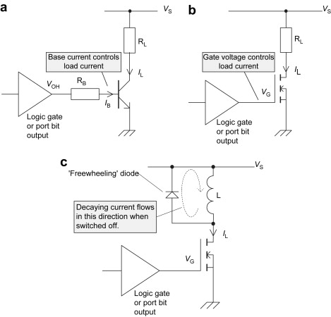
Figure 8.24 Transistor switching of DC loads. (a) Resistive, bipolar transistor. (b) Resistive, MOSFET. (c) Inductive, MOSFET
A bipolar transistor (Figure 8.24(a)) requires a small base current to switch a much larger collector current. MOSFETs (Figure 8.24(b)) require a modest gate voltage, with negligible current, to switch a large drain current. As the MOS device is purely voltage-controlled, its gate can be connected directly to the port bit output. This output must then just comfortably exceed the gate-to-source threshold voltage necessary for the MOSFET to switch on. This simplicity of connection makes the MOSFET a very attractive option for load switching in the microcontroller environment, as long as the threshold voltage just mentioned can be exceeded.
Special families of MOSFETs, designed for direct interface to logic levels, are available. Two examples, made by the company Zetex [Ref. 8.10], are shown in Table 8.1. For either transistor, it can be seen that if their gate-to-source voltage Vgs exceeds 3 V, then their drain-to-source resistance falls from near infinity to a low value. How low it goes depends on the type and internal construction. The ZVN4306A has the lower maximum ‘on’ resistance of 0.33 Ω. Its input capacitance is, however, 350 pF. The slightly lower-priced ZVN4206A has an ‘on’ resistance of 1.5 Ω, but a lesser input capacitance of 100 pF. This input capacitance has to be charged by the drive circuit as it switches from Logic 0 to 1. For high current-capacity MOSFETs it becomes a significant factor, in many cases needing its own drive circuit.
TABLE 8.1 Characteristics of two popular logic-compatible MOSFETs
| Characteristic | ZVN4206A | ZVN4306A |
|---|---|---|
| Maximum drain-to-source voltage, VDS (V) | 60 | 60 |
| Maximum gate-to-source threshold, VGS(th) (V) | 3 | 3 |
| Maximum drain-to-source resistance when ‘on’, RDS(on) (Ω) | 1.5 | 0.33 |
| Maximum continuous drain current, ID | 600 mA | 1.1 A |
| Maximum power dissipation (W) | 0.7 | 1.1 |
| Input capacitance (pF) | 100 | 350 |
If the load is inductive – like a DC motor, the winding on a stepper motor, a solenoid or electromechanical relay – then special precautions must be taken. The inductance stores energy when current is flowing in its magnetic field. If the applied voltage is switched off, it is essential for a path to be provided for the current to decay to zero, by which process the inductance returns the stored energy to the circuit. This is normally done by the inclusion of a ‘freewheeling’ diode, as seen in Figure 8.24(c).
8.9.2 Simple switching on the Derbot
The Derbot AGV uses transistor switching in a number of places, both on the main AGV as well as on the hand controller, to switch loads on and off. Two of these are shown in Figure 8.25, taken from the main Derbot circuit diagram of Figure A3.1.
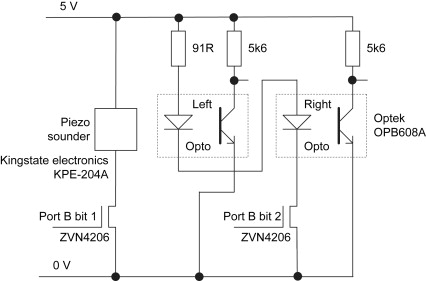
The piezo sounder is rated at 9 mA, 3–20 V. As such, it can be driven directly from the 5 V supply, so does not demand its own drive transistor. Nevertheless, to minimise loading on the microcontroller, it was decided to include one. The opto-sensors tend to be a little more power-hungry. To minimise overall current consumption, the two sensor LEDs are connected in series, as seen in the figure. Experimentally, the sensors were found to operate well if the resistor in series with the LEDs was 91 Ω. With (from the device data) a forward voltage across each diode of around 1.7 V, this indicates a current of:
As with the piezo sounder, a PIC microcontroller port output would be able to switch this, although it is closer to the 25 mA ‘absolute maximum’ limit. Again, however, it was decided to use transistor switching to minimise microcontroller loading.
8.9.3 Reversible switching: the H-bridge
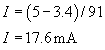
As we have seen, it is easy to switch loads on and off, with the current always going in the same direction. Some loads, however, for example DC or stepper motors, need to have a reversible voltage applied, even if only a unipolar supply voltage is available. The way this is usually achieved is by a simple yet ingenious circuit connection called the H-bridge, shown in Figure 8.26.
In the H-bridge two pairs of switching devices, usually transistors, are connected between the supply rail and 0 V. For simplicity the switching devices are shown in the diagram as switches, with a control input assumed to close the switch if the control is at Logic 1. The switch pairs are labelled A and B. Each pair has a ‘high-side’ and a ‘low-side’ switch. The load is connected between the two pairs to form an overall H configuration. Clearly, the switches in a pair must never be on at the same time or the supply will be shorted to ground. Therefore, it is common to drive them through a logic inverter, as shown, to ensure that only one can be on at any time.
If input X is switched low and input Y high, then the switch positions will be as shown in the diagram, with upper right and lower left closed and the other two open. Current will then have a path through the high-side of Pair B, through the load and through the low-side of pair A. If the two inputs are reversed, then all switches will change state and current flows in the opposite direction. Reversible current drive has been achieved. If the load is inductive, freewheeling diodes must be connected as shown. This circuit, and derivations of it, is used in many applications – from low power to very high power indeed.
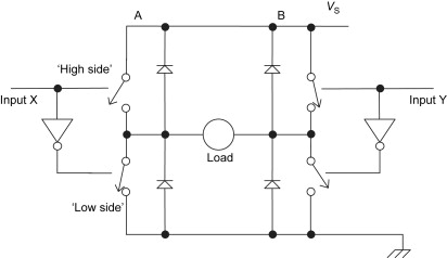
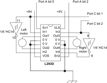
A low-power, practical realisation of the H-bridge is available in the L293D IC, made by ST Microelectronics [Ref. 8.11]. This contains four half-bridges, so that two full H-bridges can be configured. A simplified diagram is shown in Figure 8.27. This is drawn so that each half-bridge is depicted as a logic buffer. This may not seem immediately obvious, but consider in the previous diagram that when input X is high, then the voltage output from transistor pair A is high, or low when input X is low.
Buffers 1 and 2 can form one complete H-bridge, as can buffers 3 and 4. Two power supplies, VLS and VOS, are used. The former supplies the input logic, while VOS supplies the bridge itself. These two supplies can be of different values, although VOS must not be less than VLS. The logic supply could, for example, be at 5 V, with the load supply at 12 V. An enable is provided to pairs of buffers, so that all switches in the bridge can be easily switched off. Internal freewheeling diodes are included. The L293D has four ground pins, which can be soldered to a copper plane on the PCB to provide a limited amount of heat sinking.
8.9.4 Motor switching on the Derbot
The Derbot AGV uses the L293D to drive its two motors, with the circuit detail shown in Figure 8.28. Instead of having separate drives to each logic input, it uses an inverter between each. Thus, the motor is always driven in one direction or the other. However, the enable lines are each driven from a port bit, so that each motor can be disabled. The logic supply is connected to the main 5 V supply, while the output supply is taken directly from the incoming battery voltage, meaning that 9 V is available for driving the motors. Internal voltage drops in the IC, however, reduce this to closer to 7 V. The enable lines each have a pull-down resistor of value 10 kΩ, connected between them and ground, not shown in this diagram (but seen in Appendix 3). These have the important function of disabling the motors when the microcontroller is not driving these lines, for example during initialisation.
8.10 Building the Derbot
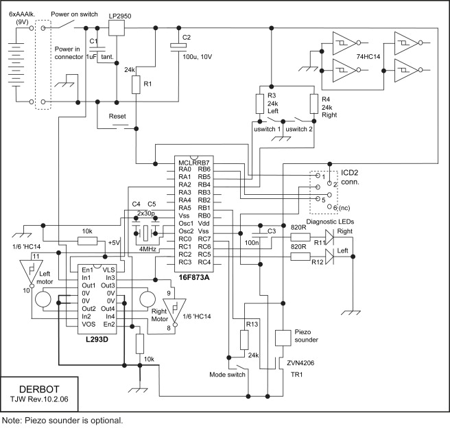
If you are building the Derbot it is suggested that you now add the motors and their drive, based around the L293D, leading to the circuit shown in Figure 8.29. If you want a running AGV, then you will also need to build the battery pack using the separate PCB and mount the spacing pillars. Further build guidance is given on the book’s companion website.
You can also at this time build up a hand controller card, either in its LED or its LCD version. The programs used in the first sections of this chapter can then be downloaded and tested. These programs do not yet cause the hand controller to interact with the AGV; this will come in later chapters.
8.11 Applying sensors and actuators – a ‘blind’ navigation Derbot program
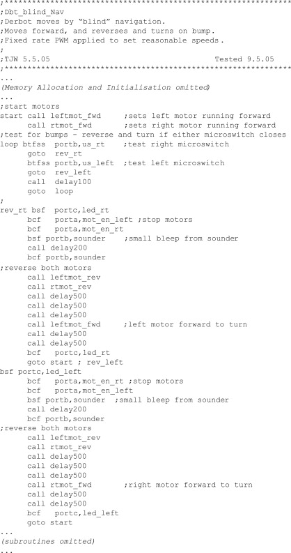
With the Derbot build as just described, it is possible to run the program Dbt_blind_Nav, as found on the book’s companion website, with the main features appearing in Program Example 8.4. This program sends the AGV running forward until it hits an obstacle, detected by its front microswitches. At this point it reverses, turns and runs forward again in a new direction.
The main program runs from the label start, by setting the motors running forward. It should be easy to do this simply by switching the motors on. However, they are chosen to give a good top speed, which is excessive for this simple application. Therefore, pulse width modulation is applied to set a slower speed. The detail of this is hidden in the subroutines leftmot_fwd and rtmot_fwd, which are called in turn. These are not included in the program example below, but can be found in the full book listing and will be fully explored in a later chapter. The program then enters a loop, at label loop. Here it repeatedly tests its microswitches and continues running until one or other is detected as being activated. When a microswitch is hit, the AGV stops, sounds the piezo sounder and reverses for 1.5 s approximately, again calling pulse width modulation subroutines to do this. It then turns, driving one motor forward while the other continues to reverse, before returning to running forward in the main program loop.
Summary
• An embedded microcontroller must be able to interface with the physical world and possibly the human world as well.
• Much human interfacing can be done with switches, keypads and displays.
• To interface with the physical world, the microcontroller must be able to interface with a range of transducers. The designer needs an understanding of the main sensors and actuators available, and must be ready to keep abreast of current technology in the field.
• Interfacing with sensors requires a reasonable knowledge of signal-conditioning techniques.
• Interfacing with actuators requires a reasonable knowledge of power-switching techniques.
8.1. 12.7 mm (0.5 inch) Single Digit Numeric Displays (2003). Kingbright, Spec. no. DSAD0006; http://www.kingbright.com.tw
8.2. HD44780 data. Available from a number of websites, including http://www.alldatasheet.com/
8.3. Interfacing PICmicro MCUs to an LCD Module (1997). Microchip Technology Inc., Application Note AN587, Ref. no. DS00587B.
8.4. Powertip; http://www.powertip.com.tw/
8.5. Silonex; http://www1.silonex.com/
8.6. Optek; http://www.optekinc.com/
8.7. Devantech. SRF04/5 data available on http://www.robot-electronics.co.uk/ and other supplier sites.
8.8. MFA/Como Drills; http://www.comodrills.com/
8.9. Futaba; http://www.futaba-rc.com/
8.10. Zetex; http://www.diodes.com/
8.11. STMicroelectronics; http://www.st.com/stonline/
Questions and exercises
1. A PIC 16F84A powered from 5 V is to drive a pulse counter display able to show 000 to 199, with the pulse input connected to pin 3. All other port pins are available for use. The two lesser digits are common-cathode 7-segment LED displays, where each segment is made up of just one LED. The ‘1’ is made up of 2 LEDs in series. All LEDs require a current of 5 mA, and at this current they have a forward voltage across them of 1.8 V. Decimal points are not used. Draw a circuit diagram for the display drive.
2. Two NORP12 LDRs are placed back-to-back in a capsule which is used to measure light direction. They are connected electrically in series, as shown in Figure 8.30, and an output voltage is taken from the junction between them. Estimate Vo:
3. Tests on a batch of OPB608A opto sensors indicate that, under ideal reflective conditions, a forward diode current of 10 mA leads to a collector current of 1.5 mA. The forward voltage across the diode is 1.7 V.
(a) Applying the circuit of Figure 8.14(b), powered from 5 V, calculate resistor values in order to give this diode current, and for this collector current to give an output voltage of 0.5 V.
(b) If the distance to the reflective surface is allowed to vary from optimum up to 0.1 inch, estimate the new collector voltage. Note: You will need to access the OPB608A data sheet to complete this part of the question.
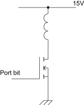
4. The circuit of Figure 8.31 shows a solenoid being switched by a ZVN4206A MOSFET, whose gate is controlled by a microcontroller port bit. The characteristics of the MOSFET are shown in Table 8.1. The resistance of the solenoid is 18.0 Ω; however, the transistor is found to fail repeatedly. Recommend changes to the circuit to make it operate reliably.
5. Design a ping-pong game, similar to the one described in Appendix 2, which displays the score of each player, based around a 16F873A microcontroller. Use Ports A and B, the same as in Appendix 2. Use a single-digit 7-segment LED display for each player, multiplexing them from Port C.
6. A model boat carries a 9 V battery and is controlled by a PIC 16F873A microcontroller. The boat has one propeller and a rudder controlled by a Futaba 3003 servo. The propeller is driven by a variable-speed DC motor with a rated maximum supply voltage of 9 V. There are two tilt switches set at right angles to each other which detect whether the boat is tilted too far from the horizontal. If the tilt is too great, the motor must be switched off. Each switch acts as an SPST (single pole single throw) switch, which is closed when no tilt is detected. Draw a design for the microcontroller circuit, in the form of a detailed circuit diagram. Include all aspects necessary to make a complete and working circuit.