Function Generators
The sources of the following circuits are contained in the Sources section, which begins on page 173. The figure number contained in the box of each circuit correlates to the source entry in the Sources section.
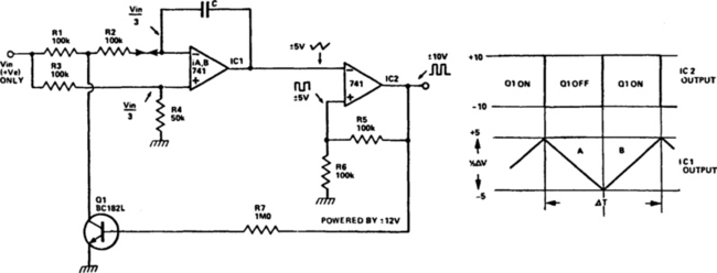
Four-Output Waveform Generator
Classic Op-Amp Astable Multivibrator
Programmable Triangle-/Square-Wave Generator
Noninteger Programmable Pulse Divider
XOR-Gate Complementary-Signals Generator
Precision Audio Waveform Generator
Easily Timed Sine-Wave/Square-Wave Oscillator
Programmable-Frequency, Free-Running Multivibrator
Programmable-Frequency Astable
Single-Control Function Generator
Triangle-/Square-Wave Generator
Wide-Range Tunable Function Generator
Sine/Cosine Generator (0.1 to 10 kHz)
Quad Op Amp Synchronized Function Generator
Oscillator or Amplifier with Wide Frequency Range
Linear Triangle-/Square-Wave VCO
Circuit for Multiplying Pulse Widths
Programmable Voltage-Controlled Frequency Synthesizer
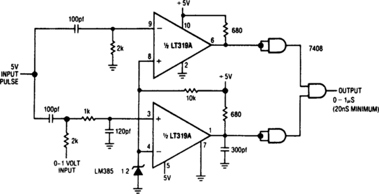
Voltage-Controlled High-Speed One Shot
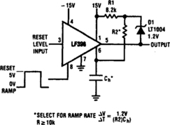
Ramp Generator with Variable Reset Level
555 Astable with Low Duty Cycle
Monostable Using Video Amplifier and Comparator
UJT Monostable Circuit Insensitive to Change in Bias Voltage
Last-Cycle Completing Gated Oscillator
Precise Triangle-/Square-Wave Generator
Wide-Range Triangle-/Square-Wave Generator
Single-Supply Function Generator
Fixed-Frequency Variable Duty-Cycle Oscillator
Wide-Range Variable Oscillator
PRECISION ONE SHOT
If you need a wide-range, resistor-programmable monostable multivibrator, you can program the circuit for pulse widths from 1 µs to 10 s (−.107:1 range). A high-to-low transition at the input causes IC1’s output to switch low, thereby turning off Q1 and Q2. With the latter transistor turned off, IC3’s output increases and the output of IC2 begins to ramp toward the negative supply level at a rate determined by the 0.01-µF capacitor and the programming resistor. When IC2’s output voltage reaches −5 V, IC3’s output switches low. If you anticipate input pulses shorter than the desired output pulses, Q3 is necessary. This transistor keeps IC1s input low while an output pulse is present, thereby preventing inadvertent resetting of the one shot.
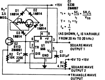
LINEAR TRIANGLE-WAVE TIMER
Using one current source for the charge and discharge path in this circuit ensures identical rise and fall times at the capacitor terminal. A Darlington pair ensures identical biasing of the IC during the charge and discharge cycles. The period of the triangle wave is: T ≈ 0.46VC1/R2. VCC must be at least 8 V to maintain linearity. At the output at pin 3 of the IC timer, a 50% duty-cycle square wave, frequency tunable by R2 alone, appears.
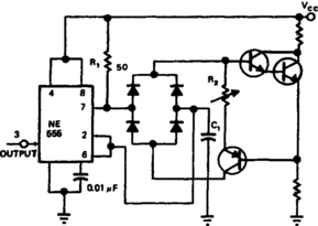
FOUR-OUTPUT WAVEFORM GENERATOR
Many applications require control signals that have phase shifts with reference to an input signal. Circuit accepts a sine, square, or triangular wave as an input reference signal and produces square-wave outputs with 0°, 90°, 180°, and 270° phase shifts with respect to the input. Figure 3-3B shows the input and output waveforms. The circuit contains two ICs: an LM565 phase-locked loop and a 7474 dual-D positive edge-triggered flip-flop. R1 and C1 set the free-running frequency of the LM565’s VCO. You should adjust R1 so that the frequency is approximately four times that of the input reference signal. The LM565 responds to input signals greater than 10 mV pk-pk; 3 V pk-pk is the chip’s maximum allowable input level. Q1 matches the LM565’s output to the flip-flops’ inputs. The flip-flops’ outputs provide the TTL-compatible square-wave signals with 0°, 90°, 180°, and 270° phase shift, with reference to the input signal.
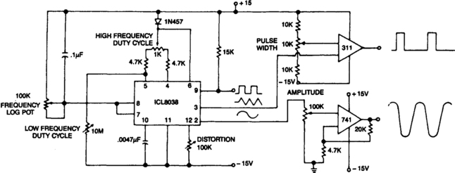
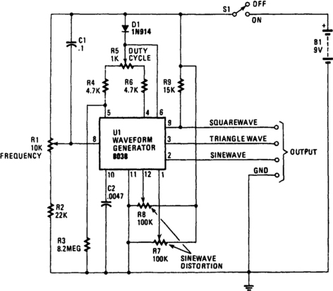
FUNCTION GENERATOR
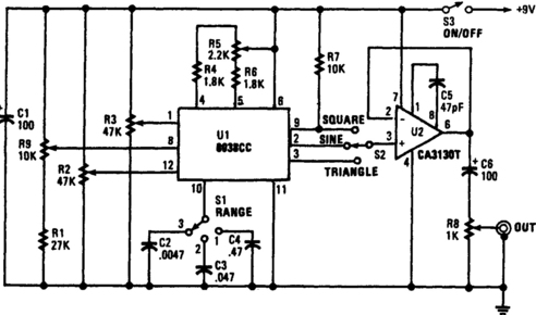
This circuit can output sine, square, and triangular signals from 15 Hz to 25 kHz in three ranges. The circuit is built around an 8038 function generator that produces the triangular- and square-wave outputs directly from an oscillator. The triangular output is then processed to develop the sine wave. While that method doesn’t provide a sufficiently low level of distortion to let you make distortion measurements on audio gear, the degree of purity is high enough for frequency-response tests and a lot of other audio analysis. Three switched capacitors, C2 to C4, set the circuits frequency range via switch S1. Variable resistor R9 and resistor R1 provide the voltage for controlling the charge and discharge rates of the timing capacitor selected. Resistors R4 to R6 control the charge and discharge currents. Resistor R5 can be adjusted to provide a 1.1 mark/space ratio.
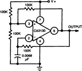
CLASSIC OP-AMP ASTABLE MULTIVIBRATOR
Uses CA3130 BiMOS op amp that operates at a frequency of 1 kHz. With rail-to-rail output swing, frequency is independent of supply voltage, device, and temperature. Only the temperature coefficient of RT and CT enters into circuit stability.
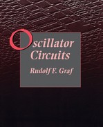
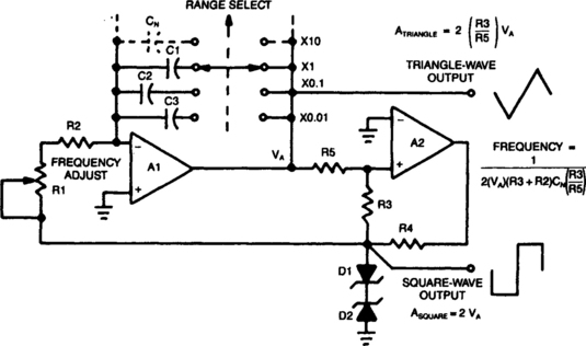
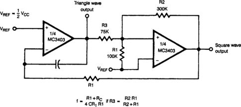
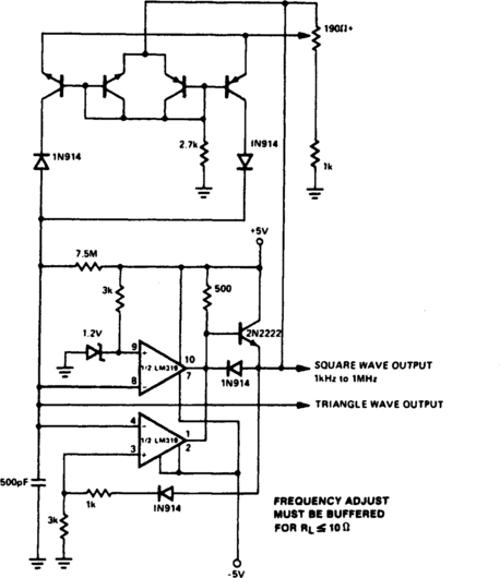
PROGRAMMABLE TRIANGLE-/SQUARE-WAVE GENERATOR
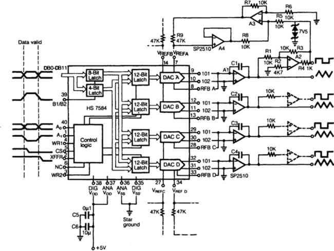
The programmable multiple output generator provides the control signals for data converter ATE. Major performance criteria are simple interfaces to a number of microprocessor systems, low power consumption, stable output timing relationships combined with a minimum of board space. For schematic simplicity only, one output circuit is shown in full.
The monolithic HS7584 provides four current output DAC’s with four quadrant multiplication, individual reference input and a feedback resistor. The digitally controlled integrator’s frequency is determined by:
C is the value of C1 to C4 and R is the resistance of the DAC. With the four DACS on a single chip, the resistance matching is good, which results in stable timing relationships of the generator outputs. The output of the comparator A2 determines whether the constant current source provided by A3 and A4 is positive or negative.
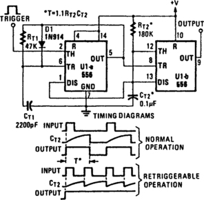
NONINTEGER PROGRAMMABLE PULSE DIVIDER
The purpose of D-type flip-flop IC2 is to synchronize the input signal with the clock pulse. When the clock pulse changes from low to high and the input is high, IC2 output is high. Subsequently, IC3 resets to zero and starts counting up. Until the counter counts to ten, the counter is inhibited. Thus, the number of pulses of the output of IC3 is ten times input pulse. The designed frequency of the clock pulse must be ten times higher than the maximum frequency of the input. IC4 and IC5 are cascaded to form a two decade programmable down counter. Since the number of pulses appearing at the input of the down counter is ten times the input to the divider, the effective range of the divisor for this divider is 0.1 to 9.9.
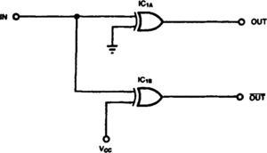
XOR-GATE COMPLEMENTARY-SIGNALS GENERATOR
Some applications, such as driving three-state buffers for data multiplexers or for biphase clocks in high-speed systems, require complementary signals having a small-time skew and nearly simultaneous transitions. Here, XOR gates function as both inverting and noninverting gates. For CMOS systems, practically any type of XOR gate will work. However, the advanced-CMOS logic (ACL) families have the greatest drive capability, the shortest gate delays, and the tightest manufacturing tolerances. For TTL systems, compatible CMOS types such as the ACT or S/AS86 families are preferable. Do not use low-power TTL, versions (LS or ALS), because they have large propagation delay differences when one XOR gate is inverting and the other is noninverting.
LOW-COST FSK GENERATOR
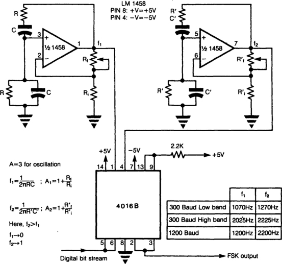
In FSK, two discrete frequencies are used to represent the binary digits 0 and 1. The heart of the circuit consists of two Wien-bridge oscillators built using a dual op amp LM 1458, for the two frequencies. The two frequencies are enabled corresponding to digital data using two switches in SCL 4016. The control lines of these switches are logically inverted with respect to each other using one of the switches in SCL 4016 as an inverter, so as to enable only one oscillator output at a time. The digital bit stream is used to control the analog switches as shown. Since the switching frequency limit of SCL 4016 is 40 MHz, high-data rates can be easily accommodated. This method comes in handy when expensive FSK generator chips are not readily available; also, the components used in this circuit are easily available off the shelf and are quite cheap.
HARMONICS GENERATOR
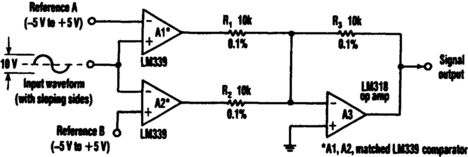
Two comparators and a summing amplifier that generate differential harmonic spectra comprise a simple frequency multiplier. The resulting circuit can extract harmonics from a sine, triangle, sawtooth, or any other sloping-sided waveform.
With a sloped-input waveform, a comparator produces an output pulse width that’s proportional to the input amplitude plus a reference voltage. Changing the reference can vary the pulse width from 0 to 100%. As the pulse width changes, the harmonic spectrum changes, but two comparators combined in the adder eliminate harmonics, depending on the duty cycle. For example, a 50% pulse will lack all the even-numbered harmonics. Similarly, a 25% duty-cycle pulse will be missing multiples of the fourth harmonic and deliver the second, sixth, and tenth harmonics. Accordingly, the circuit generates multiples of the input frequency that might not have existed in the input waveform. Adjusting the references can create virtually any harmonic.
Because comparators A1 and A2 supply differential inputs to the added A3, the adder cancels out equal harmonics. Therefore, both A1 and A2 should have identical ac characteristics, and A3 should have good common-mode rejection and a high slew rate. In particular, R1, R2, and R3 should match within 0.1%. Of course, the accuracy of the circuit depends heavily on the amplitude stability of the input.
LOW-FREQUENCY FM GENERATORS
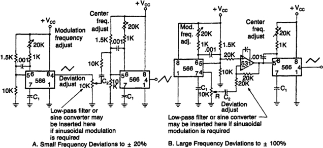
Here are two FM generators for low frequency, less than 0.5-MHz center frequency, applications. Each uses a 566 function generator as a modulation generator and a second 566 as the carrier generator. Capacitor C1 selects the modulation frequency adjustment range and C1 selects the center frequency. Capacitor C2 is a coupling capacitor which only needs to be large enough to avoid distorting the modulating waveform. If a frequency sweep in only one direction is required, the 566 ramp generators given in this section can be used to drive the center generator.
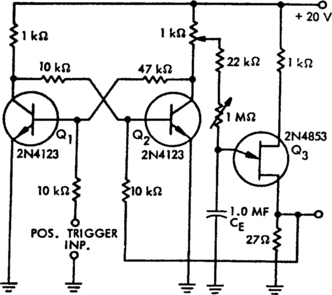
POSITIVE-TRIGGERED MONOSTABLE
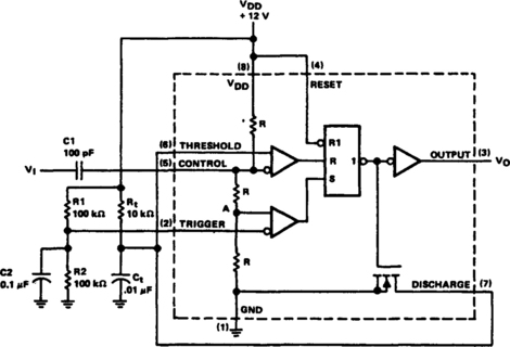
Fig. 3-12 Reprinted by permission of Texas Instruments.
A positive-going trigger pulse can be used to start the timing cycle with the circuit shown. In this design, trigger input pin 2 is biased to 6 V (½ VDD) by divider R1 and R2. Control input pin 5 is biased to 8 V (2/3 VDD) by the internal divider circuit. With no trigger voltage applied, point A is at 4 V (⅓ VDD). To turn the timer on, the voltage at point A has to be greater than the 6 V present on pin 2. Positive 5-V trigger pulse VI applied to the control input pin 5 is ac coupled through capacitor C1, adding the trigger voltage to the 8 V already on pin 5; this results in 13 V with respect to ground. The output pulse width is determined by the values of Rt and Ct.
When voltage at point A is increased to 6.5 V, which is greater than the 6 V on pin 2, the timer cycle is initialized. The output of timer pin 3 increases, turning off discharge transistor pin 7 and allowing Ct to charge through resistor Rt. When capacitor Ct charges to the upper threshold voltage of 8 V (2/3 VDD), the flip-flop is reset and output pin 3 decreases. Capacitor Ct then discharges through the discharge transistor. The timer is not triggered again until another trigger pulse is applied to control input pin 5.
PRECISION AUDIO WAVEFORM GENERATOR
This circuit generates sinusoidal, square, and triangle waveforms simultaneously. Set the frequency to a particular value or vary it, as shown above. An op amp can be added for extra drive capability and simplified amplitude adjustment. A simple comparator, slicing the triangle waveform, provides continuous duty cycle adjustment at a constant frequency.
MONOSTABLE MULTIVIBRATOR
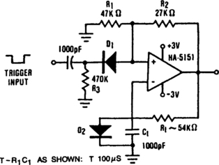
The circuit illustrates the usefulness of the HA5151 as a battery-powered monostable. In this circuit, the ratio is set to 0.632, which allows the time constant equation to be reduced to:
D2 is used to force the output to a defined state by clamping the negative input at +0.6 V. Triggering is set by Cl, R3, and D2. An applied trigger pulls the positive input below the clamp voltage, +0.6 V, which causes the output to change state. This state is held because the negative input cannot follow the change because of Rt•Ct. This particular circuit has an output pulse width set at approximately 100 µs. Use of potentiometers for Rt and variable capacitors for Ct will allow for a wide variation in T.
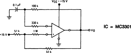
FIXED-FREQUENCY GENERATOR
A single op amp, one fourth of an LM324 quad op amp, is configured as a standard inverting amplifier. At power up, a positive voltage is applied to the noninverting input of U1, via R3, forcing its output high. That high output travels along three paths. The first path is the tone output. Along the second path, by way of R5, that high is used as the drive signal for BZ1. In the third path, the high output of U1 is fed back, via R4, to the inverting input of U1. That forces U1’s output to go low. And that low, when fed back to the inverting input of U1, causes the op amp output again to a high, and the cycle repeats itself. As configured, U1 provides a voltage gain of 4.7 (gain=R4/R1).
The outer ring of the piezo element is usually connected to the circuit ground. The large inner circle serves as the driven area, and the small elongated section supplies the feedback signal. Resistor R5 sets BZ1’s output-volume level. That level can be increased by decreasing R5 for example, to 470 Ω.
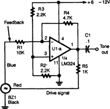
Resistors R2 and R3 set the bias for op amp U1’s positive input pin 3 to half of the supply-voltage level. That allows for a maximum voltage swing at U1’s output. Although a quad op amp is specified, almost any similar low-cost single or dual op amp will work for U1a.
SINGLE-SUPPLY MULTIVIBRATOR
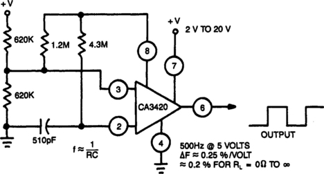
This multivibrator uses a CA3420 BiMOS op amp to provide improved frequency stability. The output frequency remains essentially independent of supply voltage. Because of the inherent buffering action of pin 6, frequency shift is approximately 0.2% when RL varies between zero Ω to infinity.
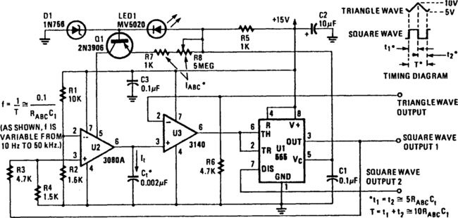
EASILY TUNED SINE-WAVE/SQUARE-WAVE OSCILLATOR
The circuit win provide both a sine- and square-wave output for frequencies from below 20 Hz to above 20 kHz. The frequency of oscillation is easily tuned by varying a single resistor. This is a considerable advantage over Wien-Bridge circuits where two elements must be tuned simultaneously to change frequency. Also, the output amplitude is relatively stable when the frequency is changed. An amp is used as a tuned circuit, driven by square wave from a voltage comparator. The frequency is controlled by R1, R2, Cl, C2, and R3, with R3 used for tuning. Tuning the filter does not affect its gain or bandwidth, so the output amplitude does not change with frequency.
A comparator is fed with the sine-wave output to obtain a square wave. The square wave is then fed back to the input of the tuned circuit to cause oscillation. Zener diode, D1, stabilizes the amplitude of the square wave fed back to the filter input. Starting is ensured by R6 and C5 which provide dc negative feedback around the comparator. This keeps the comparator in the active region. Distortion ranges between 0.75% and 2% depending on the setting of R3. Although greater tuning range can be accomplished by increasing the size of R3 beyond 1 kΩ, distortion becomes excessive. Decreasing R3 lower than 50 Ω can make the filter oscillate by itself.
ASTABLE
This astable will trigger itself and run free as a multivibrator. The external capacitor charges through RA and RB and discharges through RB only. Thus, the duty cycle is set by the ratio of these two resistors, and the capacitor charges and discharges between 1/3 Vs and 2/3 Vs. The charge and discharge times, and therefore frequency, are independent of supply voltage. The free-running frequency versus RA, RB and C is shown in the graph.
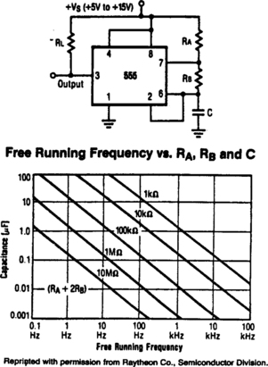
Fig. 3-19
TWO-FUNCTION SIGNAL GENERATOR
You can continuously vary the frequencies of the triangle and square waves produced by this circuit over a full decade. If R5=R3, the amplitude of the two waveforms will be equal (Asquare=ATriangle).
TRIANGLE GENERATOR
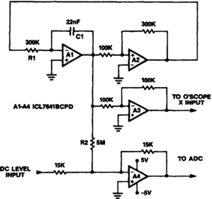
This circuit generates a symmetrical, 10-mV pk-pk triangle waveform which is summed with a dc level and connected to the a/d analog input for noise/DNL testing. The dc level input offsets the triangle waveform over the input range of the ADC. The 10-mV amplitude amounts to an 8 LSB span for a 12-bit, 5-V, full-scale ADC.
MONOSTABLE
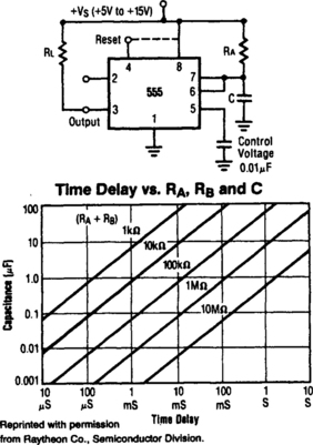
Fig. 3-22
In this mode, the timer functions as a one shot. The external capacitor is initially held discharged by a transistor internal to the timer. Applying a negative trigger pulse to pin 2 sets the flip-flop, driving the output high, and releasing the short circuit across the external capacitor. The voltage across the capacitor increases with the time constant r = RAC to 2/3 Vs, where the comparator resets the flip-flop and discharges the external capacitor. The output is now in the low state.
Circuit triggering takes place when the negative-going trigger pulse reaches ⅓ Vs; the circuit stays in the output high state until the set time elapses. The time the output remains in the high state is 1.1 RAC and can be determined by the graph. A negative pulse applied to pin 4 (reset) during the timing cycle will discharge the external capacitor and start the cycle over again beginning on the positive-going edge of the reset pulse. If reset function is not used, pin 4 should be connected to Vs to avoid false resetting.
PROGRAMMABLE-FREQUENCY, FREE-RUNNING MULTIVIBRATOR
This is the simplest of any programmable oscillator circuit, since only one stable timing capacitor is required. The output square wave is about 25 V pk-pk, and has rise and fall times of about 0.5 µs. If a programmable attenuator circuit is placed between the output and the divider network, 16 frequencies can be produced with two HA-200’s and still only one timing capacitor.
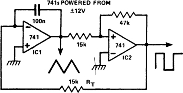
FUNCTION GENERATOR
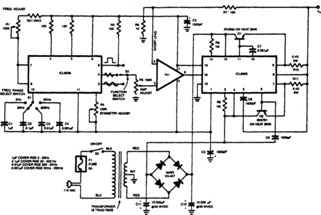
This generator will supply sine, triangular, and square waves from 2 Hz to 20 kHz. This complete test instrument can be plugged into a standard 110 Vac line for power. VOUT will be up to ± 25 V (50 V pk-pk across loads as small as 10 Ω (about 2.5 A maximum output current).
Capacitor working voltages should be greater than 50 Vdc and all resistors should be ½ W, unless otherwise indicated. The interconnecting leads from the 741 pins 2 and 3 to their respective resistors should be kept short, less than 2 inches if possible; longer leads might result in oscillation. Full output swing is possible to about 5 kHz; after that the output begins to taper off because of the slew rate of the 741, until at 20 kHz the output swing will be about 20 Vpp ± 10 V. This problem can be remedied by simply using an op amp with a higher slew rate, such as the LF356.
LOW-FREQUENCY MULTIVIBRATOR
This circuit uses half of the CA3290 BiMOS dual voltage comparator as a conventional multivibrator. The second half maintains frequency against effects of output loading. Large values of timing resistor, R1, ensure long time delays with low-leakage capacitors.
ASTABLE MULTIVIBRATOR
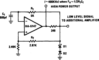
The power bandwidth of the HA-5147 extends the circuit’s frequency range to approximately 500 kHz. Rt can be made adjustable to vary the frequency if desired. Any timing errors because of V0S or Ibias have been minimized by the precision characteristics of the HA-5147. D1 and D2, if used, should be matched to prevent additional timing errors. These clamping diodes can be omitted by tying Rt, and positive feedback resistor Rf directly to the output.
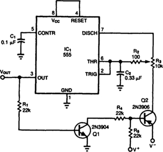
SINGLE-CONTROL FUNCTION GENERATOR
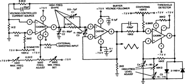
This function generator, with an adjustment range in excess of 1,000,000 to 1, uses a CA3160 BiMOS op amp as a voltage follower, a CA3080 OTA as a high-speed comparator, and a CA3080 as a programmable-current source. Three variable capacitors, C1, C2, and C3 shape the triangular signal between 500 kH and 1 MHz. Capacitors C4 and C5, and the trimmer potentiometer in series with C5, maintain essentially constant (± 10%) amplitude to 1 MHz.
TRIANGLE-/SQUARE-WAVE GENERATOR
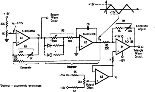
Fig. 3-31 Reprinted with permission from Raytheon Co., Semiconductor Division.
This circuit uses a positive-feedback loop closed around a combined comparator and integrator. When power is applied, the output of the comparator will switch to one of two states, to the maximum positive or maximum negative voltage. This applies a peak input signal to the integrator, and the integrator output will ramp either down or up, opposite of the input signal. When the integrator output, which is connected to the comparator input, reaches a threshold set by R1 and R2, the comparator will switch to the opposite polarity. This cycle will repeat endlessly, the integrator charging positive then negative, and the comparator switching in a square-wave fashion.
VARIABLE DUTY CYCLE TIMER
When configured as a free-running multivibrator, a 555 timer provides no more than a 50% duty cycle. By adding two transistors, however, you can obtain a variable 5 to 95% duty cycle without changing the sum of the on and off times. When VOUT decreases, Q1 is on and Q2 is off, disconnecting V + while timing capacitor C2 discharges into pin 7 of the timer. When VOUT increases, Q2 reconnects V + for recharging C2.
Adjusting linear trimming potentiometer R3 to increase the charging resistance increases the on time, but decreases the off time by the same amount by lowering the discharge resistance (the converse is also true). As a result, the sum of the on and off times remains constant. R2 protects Q2 and the timer against high-charge/discharge currents.
BASIC FUNCTION GENERATOR
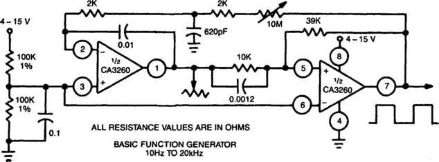
This function generator uses a CA3260 BiMOS op amp to perform both the integrator and switching functions. A 620-pF capacitor and 2-kΩ resistor shape feedback square wave to reduce spikes. Full audio spectrum, 10 Hz to 20 kHz, is covered with a single 10-Ω potentiometer. This circuit requires 9-V battery.
SAWTOOTH AND PULSE GENERATOR
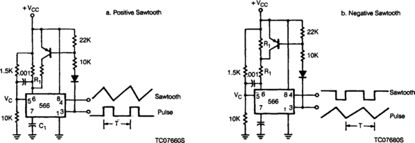
The pin 3 output of the 566 can be used to provide different charge and discharge currents for C1 so that a sawtooth output is available at pin 4 and a pulse at pin 3. The pnp transistor should be well saturated to preserve good temperature stability. The charge and discharge times can be estimated by using the formula:
where RT is the combined resistance between pin 6 and VCC for the interval considered.
SINE/COSINE GENERATOR (0.1 to 10 kHz)
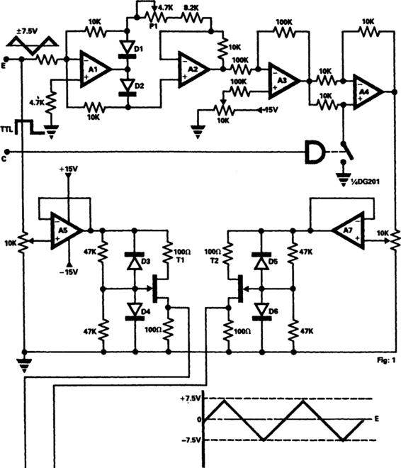
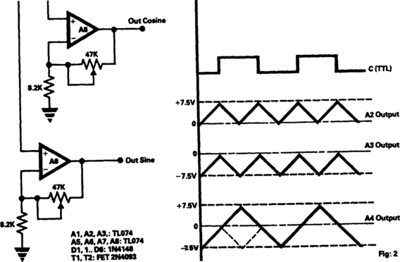
The scheme presented delivers waveforms from any function generator producing a triangular output and a synchronized TTL square wave. A1 and A2 act as a two-phase current rectifier by inverting the negative voltage appearing at the input of A1.
Positive input: Both A1 and A2 work as unity-gain followers, D1 and D2 being in the off-state.
Negative input: A1 has a −⅔ gain (D1 off and D2 on), A2 has a +3/2 gain and the total voltage transfer is −1 between output and input. P1 allows a fine trimming of the −1 gain for the negative input signals. A3 adds a continuous voltage to the rectified positive signal in order to attack A4 which acts as a ± multiplier commanded by the TTL input through the analog switch. The signal polarity is reconstructed and the output of A4 delivers a triangular waveform, shifted by 90°, with respect to the input signal (Fig. 2). The original and the shifted voltages are fed into the triangle-to-sine converters through A5 and A7, working as impedance converters. Over the frequency dynamic ranges, from 0.1 Hz to 10 kHz, the phase shift is constant and the distortion on the sine voltage is less than 1%.
QUAD OP AMP SYNCHRONIZED FUNCTION GENERATOR
A quad op amp can simultaneously generate four synchronized waveforms. The two comparators (A1 and A3) produce square and pulse waves, while the two integrators (A2 and A4) give triangular and sawtooth waves. Resistor R1 sets the duty cycle and the frequency, along with resistors R and capacitors C.
OSCILLATOR OR AMPLIFIER WITH WIDE FREQUENCY RANGE
An oscillator/amplifier is resistively tunable over a wide frequency range. Feedback circuits containing operational amplifiers, resistors, and capacitors synthesize the electrical effects of an inductance and capacitance in parallel between the input terminals. The synthetic inductance and capacitance, and, therefore, the resonant frequency of the input admittance, are adjusted by changing a potentiometer setting. The input signal is introduced in parallel to the noninverting input terminals of operational amplifiers A1 and A2 and to the potentiometer cursor. The voltages produced by the feedback circuits, in response to input voltage, V1 are indicated at the various circuit nodes.
LINEAR TRIANGLE-/SQUARE-WAVE VCO
The VCO has two buffered outputs; a triangle wave and a square wave. The frequency is dependent on the output voltage swing of the Schmitt trigger, IC2. Superior performance can be obtained by replacing Q1 with a switching FET. Fast FET op amps will improve high-frequency performance.
CIRCUIT FOR MULTIPLYING PULSE WIDTHS
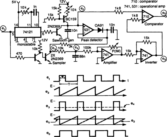
A circuit for multiplying the width of incoming pulses by a factor of greater or less than unity is simple to build. Also, the multiplying factor can be selected by adjusting one potentiometer only. The multiplying factor is determined by setting the potentiometer P in the feedback of a 741 amplifier. The input pulses e1 of width τ and repetition period T is used to trigger a sawtooth generator at its rising edges to produce the waveform e2 having a peak value of (E) volt. This peak value is then sampled by the input pulses to generate the pulse train e3 having an average value of e4(= E Eτ/T), which is proportional to τ and independent on T. The dc voltage e4 is amplified by a factor k and compared with sawtooth waveform e2 giving output pulses of duration k τ. The circuit is capable of operating over the frequency range 10 to 100 kHz.
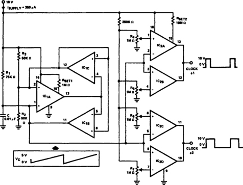
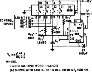
PROGRAMMABLE VOLTAGE-CONTROLLED FREQUENCY SYNTHESIZER
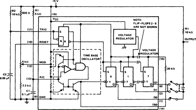
The μA2240 consists of four basic circuit elements: (1) a time-base oscillator, (2) an eight-bit counter, (3) a control flip-flop, and (4) a voltage regulator. The basic frequency of the time-base oscillator (TBO) is set by the external time constant, which is determined by the values of R1 and C1 (1?R1C1=2 kHz). The open-collector output of the TBO is connected to the regulator output via a 20-kΩ pull-up resistor, and drives the input to the eight-bit counter. At power-up, a positive trigger pulse is detected across C2 which starts the TBO and sets all counter outputs to a low state. Once the μA2240 is initially triggered, any further trigger inputs are ignored until it is reset. In this astable operation, the μA2240 will free-run from the time it is triggered until it receives an external reset signal. Up to 255 discrete frequencies can be synthesized by connecting different counter outputs.
EMITTER-COUPLED RC OSCILLATOR
The circuit covers 15 Hz to 30 kHz and is useful as a function generator. The 2N2926 or equivalent transistors can be used.
555 ASTABLE WITH LOW DUTY CYCLE
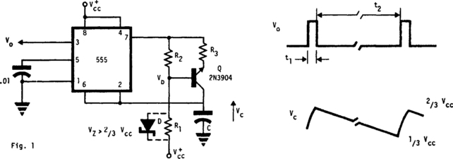
This free-running multivibrator uses an external current sink to discharge the timing capacitor, C. Therefore, interval t2 can easily be 1000 × the pulse duration, t1, which defines a positive output. Capacitor voltage, VC, a negative-going ramp with exponential rise during the pulse output periods.
MONOSTABLE USING VIDEO AMPLIFIER AND COMPARATOR
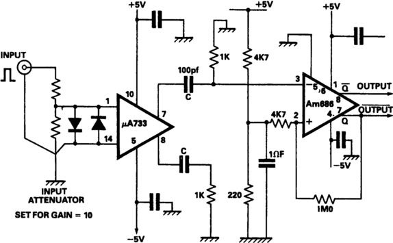
The output of a video amplifier is differentiated before being fed to a Schottky comparator. The propagation delay is reduced to typically 10 ns. The output pulse width is set by the value of C; 100 pf gives a pulse of about 90 ns duration.
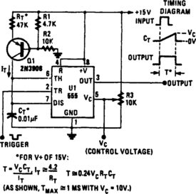
LINEAR RAMP GENERATOR
The linear charging ramp is most useful where linear control of voltage is required. Some possible applications are a long-period voltage-controlled timer, a voltage-to-pulse width converter, or a linear pulse width modulator. Q1 is the current source transistor, supplying constant current to the timing capacitor Ct. When the timer is triggered, the clamp on Ct is removed and Ct charges linearly toward VCC by virtue of the constant current supplied by Q1. The threshold at pin 6 is ⅔ VCC; here, it is termed VC. When the voltage across Ct reaches VC volts, the timing cycle ends. The timing expression for output pulse with T is:
In general, It, should be at 1-mA, compatible with the NE555.
WAVEFORM GENERATOR
The circuit is designed around the Intersil 8038CC. Frequency range is approximately 20 Hz to 20 kHz—a tuning range of 1000:1 with a single control. The output frequency depends on the value of C2 and on the setting of potentiometer R1. Other values of C2 change the frequency range. Increase the value of C2 to lower the frequency. The lowest possible frequency is around 0.001 Hz and the highest is around 300 kHz.
LAST-CYCLE COMPLETING GATED OSCILLATOR
Regenerative feedback at C enables the oscillator to complete its timing cycle, rather than immediately shutting it off. The IC used was a CD4011AE, although an equivalent will work.
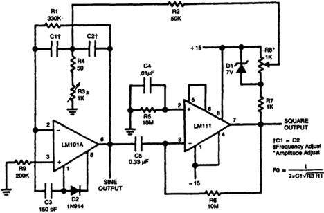
PRECISE TRIANGLE-/SQUARE-WAVE GENERATOR
Since the output range swings exactly from rail to rail, frequency and duty cycle are virtually independent of power supply variations.
WAVEFORM GENERATOR
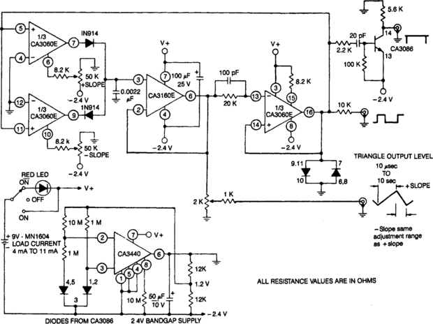
The circuit uses a CA3060 triple OTA (two units serve as switched current generators, controlled by a third amplifier). A CA3160 BiMOS op amp serves as a voltage follower to buffer the 0.0022-µF integrating capacitor. The circuit has an adjustment range of 1,000,000:1 and a timing range of 20 µs to 20 sec. The on-off switch actuates an LED that serves, as both a pilot light and a low-battery indicator. The LED extends battery life, because it drops battery voltage to the circuit by approximately 1.2 volts, thus reducing supply-current.
SINGLE-SUPPLY FUNCTION GENERATOR
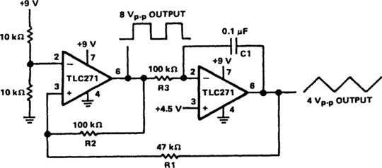
This circuit has both square-wave and triangle-wave outputs. The left section is similar in function to a comparator circuit that uses positive feedback for hysteresis. The inverting input is biased at one-half the VCC voltage by resistors R4 and R5. The output is fed back to the noninverting input of the first stage to control the frequency. The amplitude of the square wave is the output swing of the first stage, which is 8 V peak-to-peak. The second stage is basically an op-amp integrator. Resistor R3 is the input element and capacitor C1 is the feedback element. The ratio R1/R2 sets the amplitude of the triangle wave, as referenced to the square-wave output. For both waveforms, the frequency of oscillation can be determined by the equation:
The output frequency is approximately 50 Hz with the given components.
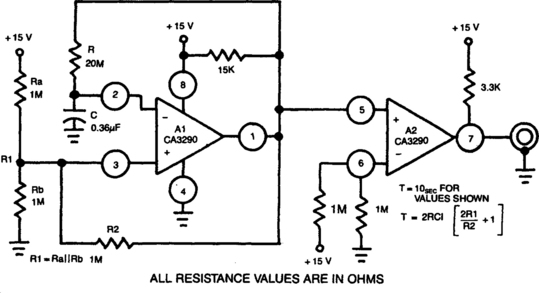
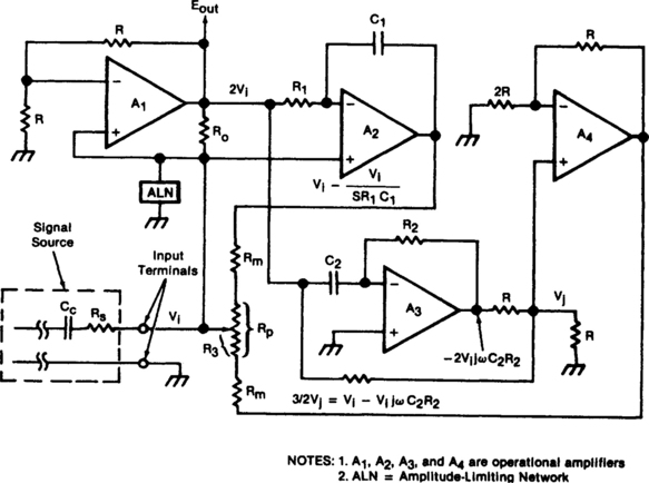
PRECISE WAVE GENERATOR
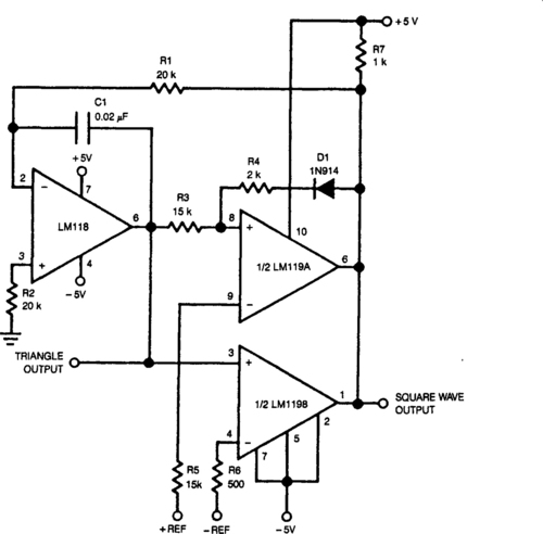
The positive and negative peak amplitude is controllable to an accuracy of about ± 0.01 V by a dc input. Also, the output frequency and symmetry are easily adjustable. The oscillator consists of an integrator and two comparators—one comparator sets the positive peak and the other sets the negative peak of the triangle wave. If R1 is replaced by a potentiometer, the frequency can be varied over at least a 10-to-1 range without affecting amplitude. Symmetry is also adjustable by connecting a 50-kΩ resistor from the inverting input of the LM118 to the arm of the 1-kΩ potentiometer. The ends of the potentiometer are connected across the supplies. Current for the resistor either adds or subtracts from the current through R1, which changes the ramp time.
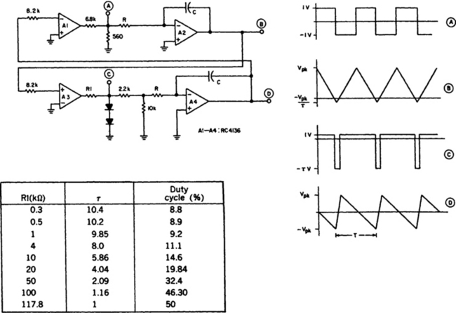
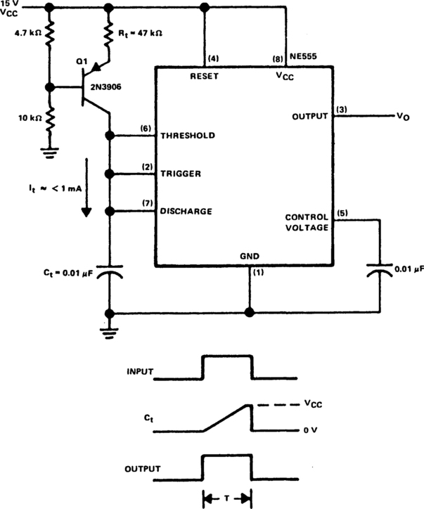
FIXED-FREQUENCY VARIABLE DUTY-CYCLE OSCILLATOR
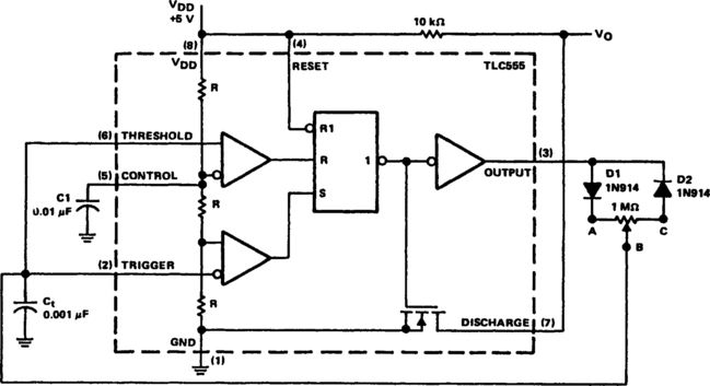
Fig. 3-58 Reprinted by permission of Texas Instruments.
In a basic astable timer, configuration timing periods t1 and t2 are not controlled independently. The lack of control makes it difficult to maintain a constant period, T, if either t1 or t2 is varied. In this circuit, charge RAB and discharge RBC resistances are determined by the position of common wiper arm B of the potentiometer. So, it is possible to adjust the duty-cycle by adjusting t1 and t2 proportionately, without changing period T.
At start-up, the voltage across Ct is less than the trigger level voltage (½ VDD), causing the timer to be triggered via pin 2. The output of the timer at pin 3 increases, turning off the discharge transistor at pin 7 and allowing Ct to charge through diode D1 and resistance Rab. When capacitor Ct charges to upper threshold voltage 2/3 VDD, the flip-flop is reset and the output at pin 3 decreases. Capacitor Ct then discharges through diode D2 and resistor RBC. When the voltage at pin 2 reaches ⅓ VDD, the lower threshold or trigger level, the timer triggers again and the cycle is repeated. In this circuit, the oscillator frequency remains fixed and the duty cycle is adjustable from less than 0.5% to greater than 99.5%.
SINGLE-CONTROL FOUR-DECADE VARIABLE OSCILLATOR
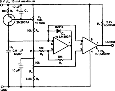
The circuit consists of a variable current source that charges a capacitor, which is rapidly discharged by a Schmitt-trigger comparator. The sawtooth waveform thus produced is fed to another comparator, one with a variable switching level. The output from the second comparator is a pulse train with an independently adjustable frequency and duty cycle. The variable-frequency ramp generator consists of capacitor C1, which is charged by a variable and nonlinear current source. The latter comprises a 2N2907A pnp transistor, plus resistor R1 and the potentiometer R2. Capacitor C2 eliminates any ripple or noise at the base of the transistor that might cause frequency jitter at the output.
SIMPLE TRIANGLE SQUARE-WAVE OSCILLATOR
This circuit generates simultaneously, a triangle and a square waveform. It is self-starting and has no latch-up problems. IC1 is an integrator with a slew rate which is determined by CT and RT, and IC2 is a Schmitt trigger. The output of IC1 ramps up and down between the hysteresis levels of the Schmitt, the output of which drives the integrator. By making RT variable, it is possible to alter the operating frequency over a 100-to-1 range. Three resistors, one capacitor, and a dual op amp is all that is needed to make a versatile triangle- and square-wave oscillator with a possible frequency range of 0.1 Hz to 100 kHz.