Multivibrators and Square-Wave Oscillators
The sources of the following circuits are contained in the Sources section, which begins on page 173. The figure number contained in the box of each circuit correlates to the source entry in the Sources section.
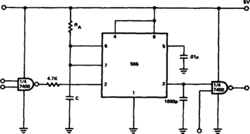
Free-Running Square-Wave Oscillator
Simple Triangle-/Square-Wave Oscillator
Adjustable TTL Clock (Maintains 50% Duty Cycle)
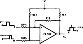
Monostable Multivibrator with Input Lock-Out
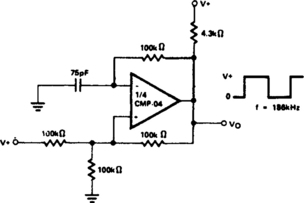
100-kHz Free-Running Multivibrator
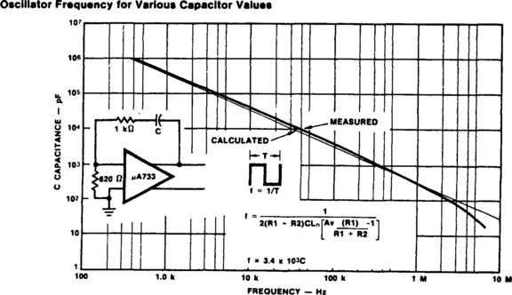
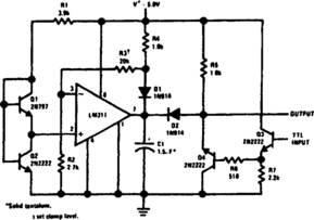
TTL OSCILLATOR
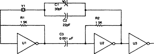
TTL inverter stages, U1 and U2, are cross-connected with a crystal Y1. A resistor in each stage biases the normally digital gates into a region where they operate as amplifiers. Inverter stage U3 is used as a buffer.
OSCILLATOR/CLOCK GENERATOR
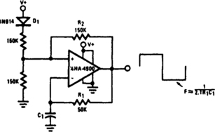
This self-starting fixed frequency oscillator circuit gives excellent frequency stability. R1 and C1 compose the frequency determining network while R2 provides the regenerative feedback. Diode D1 enhances the stability by compensating for the difference between VOH VSupply. In applications where a precision clock generator up to 100 kHz is required, such as in automatic test equipment, C1 can be replaced by a crystal.
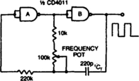
CMOS OSCILLATOR
Varying the 100-kΩ pot changes the discharge rate of CT and hence the frequency. A square-wave output is generated. The maximum frequency using CMOS is limited to 2 MHz.
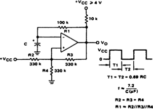
SIMPLE TRIANGLE-/SQUARE-WAVE OSCILLATOR
By making RT variable it is possible to alter the operating frequency over a 100-to-1 range. Versatile triangle-/square-wave oscillator has a possible frequency range of 0.1 Hz to 100 kHz.
ADJUSTABLE TTL CLOCK (MAINTAINS 50% DUTY CYCLE)
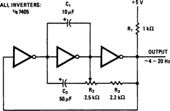
Symmetry of the square-wave output is maintained by connecting the right side of R2 through resistor R3 to the output of the third amplifier stage. This changes the charging current to the capacitors in proportion to the setting of frequency-adjusting potentiometer R2. Thus, a duty cycle of 50% is constant over the entire range of oscillation. The lower frequency limit is set by capacitor C2. With the components shown, the frequency of oscillation can be varied by R2 from about 4 to 20 Hz. Other frequency ranges can be obtained by changing the values of C1 and R3, which control the upper limit of oscillation, or C2, which limits the low-frequency end.
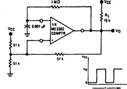
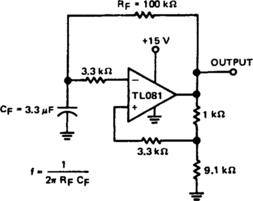
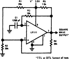
SQUARE-WAVE OSCILLATOR
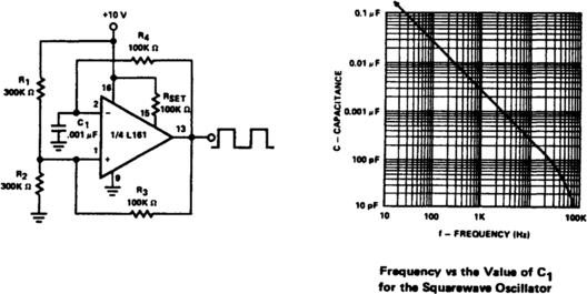
This generator is operable to over 100 kHz. The low frequency limit is determined by C1. Frequency is constant for supply voltages down to + 5 V.
DUAL ASTABLE MULTIVIBRATOR
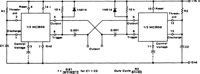
This dual astable multivibrator provides versatility not available with single-timer circuits. The duty cycle can be adjusted from 5% to 95%. The two outputs provide two phase clock signals often required in digital systems. It can also be inhibited by use of either reset terminal.
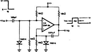
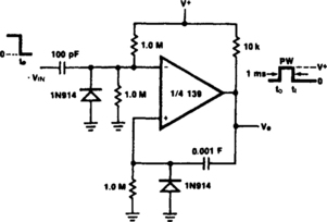
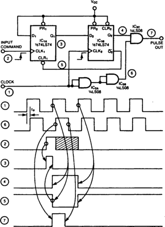
SQUARE-WAVE PULSE EXTRACTOR
This circuit traps a single positive pulse from a square-wave train. Following the rising edge of an input command, the pulse-out signal emits a replica of one positive pulse of the clock signal simultaneous with the clock signal’s next rising edge. The input command signal sets the Q1 output of flip-flop IC1A. Consequently, the next rising edge of the clock signal sets the Q2 output of IC1B, which allows AND gate IC2C to pass the clock signal’s next positive pulse. AND gates IC2A and IC2B prevent the generation of brief output glitches by delaying the clock signal by tD seconds (two propagation delays).
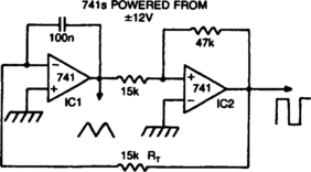
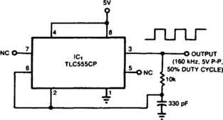
NEARLY 50% DUTY-CYCLE MULTIVIBRATOR
Three factors contribute to the output symmetry. The capacitor charges and discharges through the same external resistor. An internal resistive divider sets accurate switching thresholds within the chip, the bipolar types use dividers, as well. Most importantly, IC1’s CMOS output stage switches fully between ground and VCC, avoiding the errors from asymmetry that are often found in a TTL timer’s output. The IC’s internal switching threshold tolerances can cause a deviation of several percent from the desired 50% duty cycle. To meet a tighter specification, you might have to select from a group of ICs.
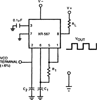
HIGH-CURRENT OSCILLATOR
The oscillator output of the XR-567 can be amplified using the output amplifier and high-current logic output available at pin 8. In this manner, the circuit can switch 100-mA load currents without sacrificing oscillator stability. The oscillator frequency can be modulated over ± 6% in frequency by applying a control voltage of pin 2.
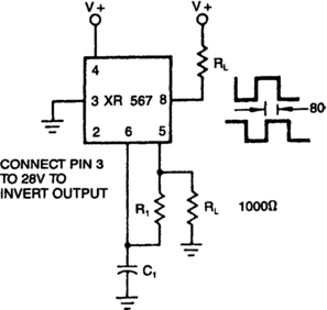
QUADRATURE-OUTPUTS OSCILLATOR
The XR-567 functions as a precision oscillator with two separate square-wave outputs at pins 5 and 8, that are at nearly quadrature phase with each other. Because of the internal biasing arrangement, the actual phase shift between the two outputs is typically 80%.
ASTABLE MULTIVIBRATOR
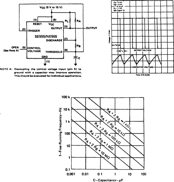
The capacitor C will charge through RA and RB, and then discharge through RB only. The duty cycle may be controlled by the values of RA and RB.
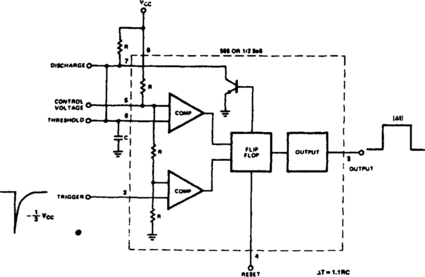
MONOSTABLE CIRCUIT
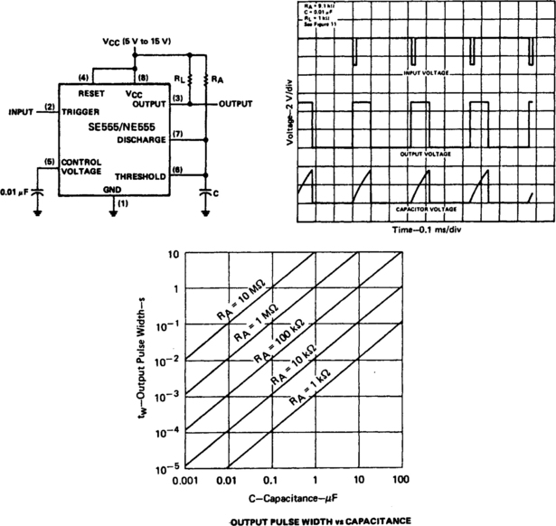
If the output is low, application of a negative-going pulse to the trigger input sets the flip-flop (Q goes low), drives the output high, and turns off 1. Capacitor C is then charged through RA until the voltage across the capacitor reaches the threshold voltage of the threshold input. If the trigger input has returned to a high level, the output of the threshold comparator will reset the flip-flop (Q goes high), drive the output low, and discharge C through Q1. Monostable operations is initiated when the trigger input voltage falls below the trigger threshold. Once initiated, the sequence will complete only if the trigger input is high at the end of the timing interval.
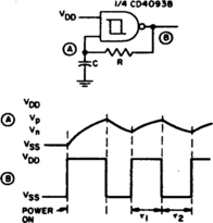
ASTABLE OSCILLATOR
Before power is applied, the input and output are at ground potential and capacitor C is discharged. On power-on, the output goes high (VDD) and C charges through R until V is reached; the output then goes low (VSS). C is now discharged through R until Vn is reached. The output then goes high and charges C toward Vp through R. Thus, input A alternately swings between Vp and Vn as the output goes high and low. This circuit is self-starting at power-on.