Crystal Oscillators
The sources of the following circuits are contained in the Sources section, which begins on page 173. The figure number contained in the box of each circuit correlates to the source entry in the Sources section.
Fundamental-Frequency Crystal Oscillator
Easy Start-Up Crystal Oscillator
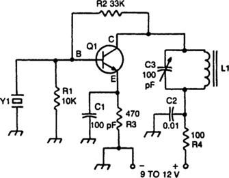
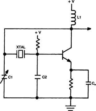
Crystal-Controlled Transistor Oscillator
Pierce Harmonic Oscillator (20 MHz)
Butler Emitter-Follower Oscillator (20 MHz)
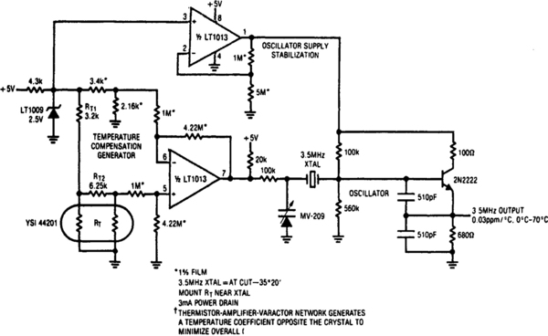
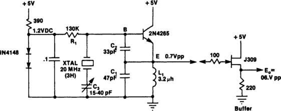
Low-Power, 5-V Driven Temperature-Compensated Crystal Oscillator (TXCO)
Crystal-Controlled Local Oscillator for SSB Transmitters
Temperature-Compensated Crystal Oscillator
100-MHz VHF Crystal Oscillator
Crystal-Controlled Reflection Oscillator
Temperature-Compensated Crystal Oscillator
High-Frequency Crystal Oscillator
Butler Emitter-Follower Oscillator (100 MHz)
Colpitts Harmonic Oscillator (Basic Circuit)
Colpitts Harmonic Oscillator (100 MHz)
International Crystal OF-1 Lo Oscillator
Parallel-Mode Aperiodic Crystal Oscillator
Voltage-Controlled Crystal Oscillator
High-Frequency Crystal Oscillator
Crystal-Controlled Oscillator Operates from One Mercury Cell
Low-Frequency Crystal Oscillator (10 to 150 kHz)
IC-Compatible Crystal Oscillator
Crystal Oscillator Provides Low Noise
Simple CMOS Crystal Oscillator
Low-Frequency Pierce Oscillator
Overtone Oscillator with Crystal Switching
Crystal-Controlled Butler Oscillator
Schmitt Trigger Crystal Oscillator
Overtone Oscillator (50 to 100 MHz)
Miller Oscillator (Crystal Controlled)
Butler Emitter-Follower Oscillator (Basic Circuit)
Butler Common-Base Oscillator (Basic Circuit)
Pierce Harmonic Oscillator (100 MHz)
International Crystal OF-1 Hi Oscillator
Standard Crystal Oscillator for 1 MHz
TTL-Compatible Crystal Oscillator
Third-Overtone Crystal Oscillator
Low-Frequency Crystal Oscillator
Varactor-Tuned 10-MHz Ceramic Resonator Oscillator
Pierce Harmonic Oscillator (Basic Circuit)
Crystal-Controlled Sine-Wave Oscillator
Stable Low-Frequency Crystal Oscillator
JFET Pierce Crystal Oscillator
Crystal-Controlled Signal Source
High-Frequency Signal Generator
Crystal-Stabilized IC Timer Can Provide Subharmonic Frequencies
FUNDAMENTAL-FREQUENCY CRYSTAL OSCILLATOR
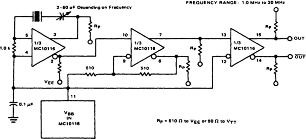
Fig. 2-1 Copyright of Motorola, Inc. Used by permission.
For frequencies below 20 MHz, a fundamental-frequency crystal can be used and the resonant tank is no longer required. Also, at this lower frequency range the typical MECL 10,000 propagation delay of 2 ns becomes small compared to the period of oscillation, and it becomes necessary to use a noninverting output. Thus, the MC10116 oscillator section functions simply as an amplifier. The 1.0 kΩ resistor biases the line receiver near VBB and the 0.1-µF, capacitor is a filter capacitor for the VBB supply. The capacitor, in series with the crystal, provides for minor frequency adjustments. The second section of the MC10116 is connected as a Schmitt-trigger circuit; this ensures good MECL edges from a rather slow, less than 20-MHz input signal. The third stage of the MC10116 is used as a buffer and to give complementary outputs from the crystal oscillator circuit. The circuit has a maximum operating frequency of approximately 20 MHz and a minimum of approximately 1 MHz; it is intended for use with a crystal which operates in the fundamental mode of oscillation.
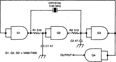
EASY START-UP CRYSTAL OSCILLATOR
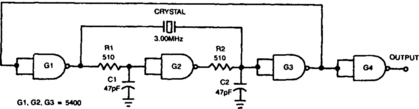
This low cost, crystal-controlled oscillator uses one TTL gate. Two factors ensure oscillator start-up: The connection of NAND gates G1, G2, and G3 into an unstable logic configuration and the high loop gain of the three inverters. Values of R1, R2, C1, and C2 aren’t critical; select them so the oscillator operates at a frequency 70 to 90% higher than the crystal frequency when the crystal is disconnected. For 1–2 MHz operation, a low-power 54L00 IC is recommended; for a 2–6 MHz, a standard 5400 type; and for 6–20 MHz, a 54H00 or 54S00.
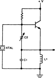
PIERCE HARMONIC OSCILLATOR (20 MHz)
This circuit has excellent short-term frequency stability because the external load tied across the crystal is mostly capacitive rather than resistive, giving the crystal a high in-circuit Q.
COLPITTS OSCILLATOR
This circuit will operate with fundamental-mode crystals in the range of 1 to 20 MHz. Feedback is controlled by capacitor voltage divider C2/C3. The rf voltage across the emitter resistor provides the basic feedback signal.
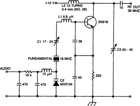
CRYSTAL-CONTROLLED LOCAL OSCILLATOR FOR SSB TRANSMITTERS
This oscillator can contain several switched crystals to provide channelized operation. A buffer amplifier can be added, if desired.
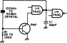
CRYSTAL-CONTROLLED OSCILLATOR
This circuit oscillates without the crystal. With the crystal in the circuit, the frequency will be that of the crystal. The circuit has good starting characteristics—even with the poorest crystals.
PIERCE OSCILLATOR
The oscillator transistor is Q1, and the crystal is placed between the collector and base. Feedback is improved by the use of the collector-emitter capacitor C2. Transistor Q2 is used as an output buffer.
CMOS CRYSTAL OSCILLATOR
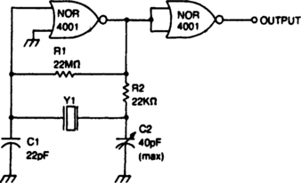
This circuit has a frequency range of 0.5 to 2.0 MHz. Frequency can be adjusted to a precise value with trimmer capacitor C2. The second NOR gate serves as an output buffer.
TEMPERATURE-COMPENSATED CRYSTAL OSCILLATOR
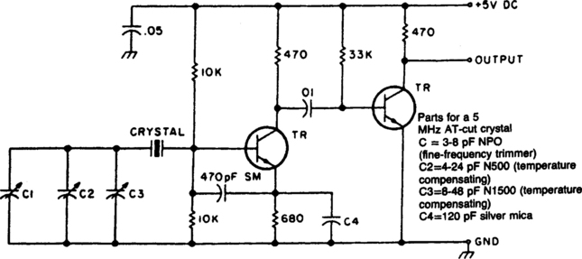
Two different negative-coefficient capacitors are blended to produce the desired change in capacitance to counteract or compensate for the decrease in frequency of the “normal” AT-cut characteristics.
CRYSTAL OSCILLATOR
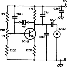
This circuit provides reliable oscillation and an output close to one volt peak-to-peak. Power consumption is around 1 mA from a 9-V supply.
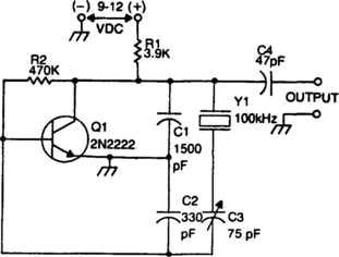
100-kHz CRYSTAL CALIBRATOR
This circuit is often used by amateur radio operations, shortwave listeners, and other operators of shortwave receivers to calibrate the dial pointer. The oscillator operates at a fundamental frequency of 100 kHz, and the harmonics are used to locate points on the shortwave dial, provided that the output of the calibrator is coupled to the antenna circuit of the receiver. The crystal shunts the feedback-voltage divider, and is in series with a variable capacitor (C3) that is used to set the actual operating frequency of the calibrator.
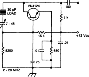
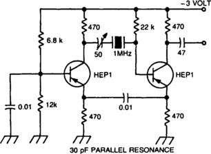
OVERTONE CRYSTAL OSCILLATOR
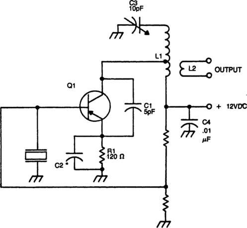
The crystal element in this circuit is connected directly between the base and ground. Capacitor C1 is used to improve the feedback due to the internal capacitances of the transistor. This capacitor should be mounted as close as possible to the case of the transistor. The LC tank circuit in the collector of the transistor is timed to the overtone frequency of the crystal. The emitter resistor capacitor must have a capacitive reactance of approximately 90-Ω at the frequency of operation. The tap on inductor L1 is used to match the impedance of the collector of the transistor. In most cases, the optimum placement of this tap is approximately one-third from the cold end of the coil. The placement of this tap is a trade-off between stability and maximum power output. The output signal is taken from a link coupling coil, L2, and operates by transformer action.
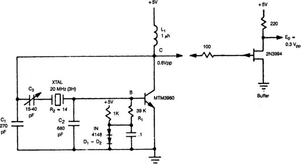
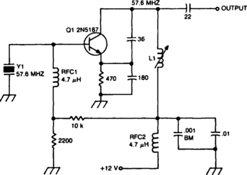
20-MHz VHF CRYSTAL OSCILLATOR
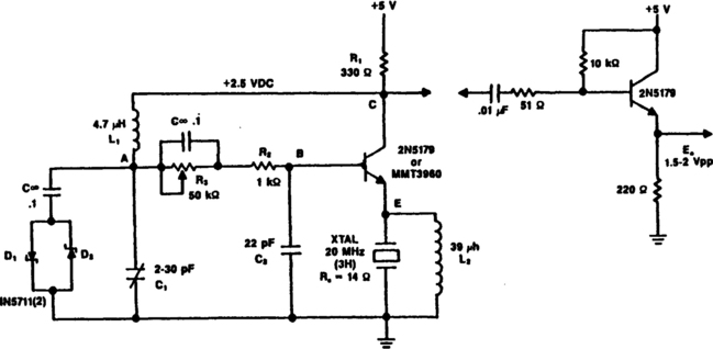
Fig. 2-16 R. Matthys, RF Design, March 1987, P 31.
A typical circuit at 20 MHz is shown. The crystal, which has an internal series resistance Rs of 14 Ω, oscillates at its third harmonic. The diode clamp D1 and D2 provides a constant amplitude control. The transistor operates continuously in a linear mode over a complete cycle of oscillation, and reflects a reasonably constant load across the crystal at all times.
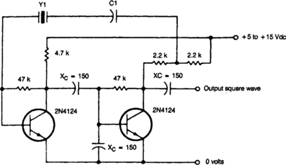
MARKER GENERATOR
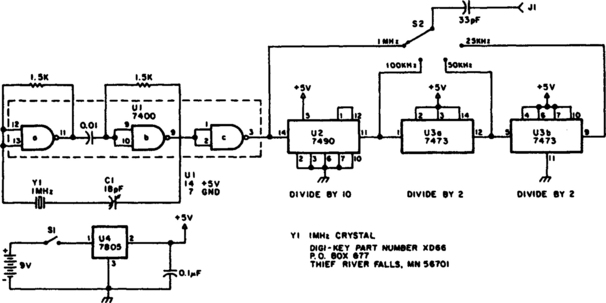
The oscillator section uses three sections of a 7400 quad NAND gate integrated circuit. The 1-MHz signal from the oscillator is fed into a 7490 decade counter configured to divide by ten, providing the 100kHz signal. To obtain the 50 and 25 kHz outputs, the 100-kHz signal is further divided by 7473 dual J-K flip-flop. The first half of the 7473 divides the 100-kHz signal by two, yielding the 50 kHz signal. The second half of the 7473 again divides by two, giving the 25 kHz signal. S2 selects the output, a square wave, rich in harmonics. The generator can be powered from any convenient 6 to 12 Vdc source. A 7805 fixed-voltage regulator supplies the regulated voltage for the oscillator and the divider chips. The generator described here is powered by a 9-V transistor radio battery.
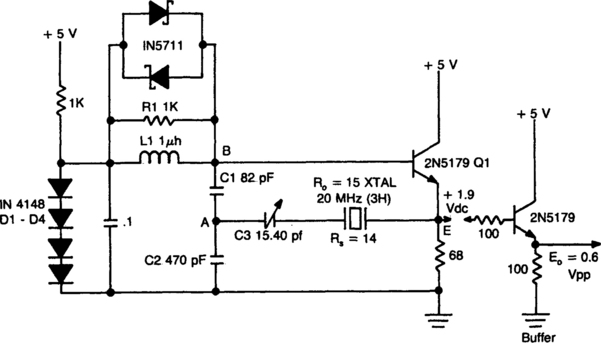
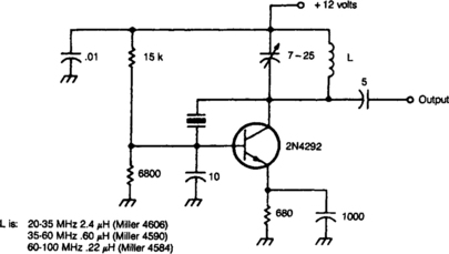
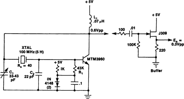
100-MHz VHF CRYSTAL OSCILLATOR
Figure 2-18 shows a 100-MHz oscillator operating on the fifth harmonic. Again to maintain the transistor’s gain, note the increase in the collector’s load resistance R1 because of the increase in the quartz crystal’s internal series resistance Rs. C3 is needed at frequencies above 50 MHz to tune out the shunting effect of L1 on R1, to maintain a high load resistance for the transistor and get enough gain for oscillation. The equivalent series RLCL, load across the crystal is 8.2 Ω (RL) and 200 pF (CL).
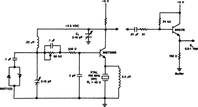
Fig. 2-18 R. Matthys, RF Design, March 1987, p. 31.
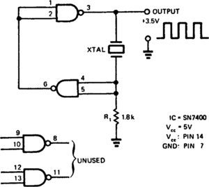
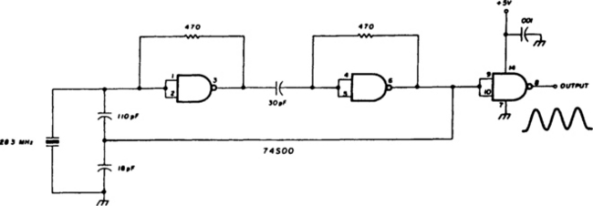
TWO-GATE QUARTZ OSCILLATOR
A SN7400 quartz crystal and a resistor provide a square-wave output of approximately 3.5 V. The circuit operates reliably at frequencies from 120 kHz to 4 MHz.
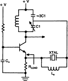
CRYSTAL-CONTROLLED REFLECTION OSCILLATOR
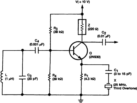
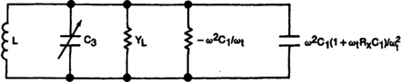
This unit is easily tunable and stable, consumes little power, and costs less than other types of oscillators that operate at the same frequencies. This unusual combination of features is made possible by a design concept that includes operation of the transistor well beyond the 3 dB frequency of its current-versus-frequency curve. The concept takes advantage of newly available crystals that resonate at frequencies up to about 1 GHz.
The emitter of transistor Q is connected with variable capacitor C1 and series-resonant crystal X. The emitter is also connected to ground through bias resistor R1. The base is connected to the parallel combination of inductor L and capacitor C3 through dc-blocking capacitor and C4 and is forward biased with respect to the emitter by resistors R3 and R4. Impedance Z could be the 220-Ω resistor shown or any small impedance that enables the extraction of the output signal through coupling capacitor C2. If Z is a tuned circuit, it is tuned to the frequency of the crystal.
TEMPERATURE-COMPENSATED CRYSTAL OSCILLATOR
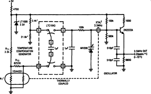
This circuit uses LTC1043 to differentiate between a temperature sensing network and a dc reference. The single-ended output biases a varactor-tuned crystal oscillator to compensate drift. The varactor crystal network has high dc impedance, eliminating the need for an LTC1043 output amplifier.
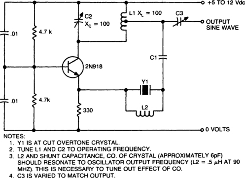
OVERTONE CRYSTAL OSCILLATOR
This circuit employs an adjustable resonant tank circuit that ensures operation at the desired crystal overtone. C1 and L1 form the resonant tank circuit, which with the values specified as a resonant frequency, are adjustable from approximately 50 to 100 MHz. Overtone operation is accomplished by adjusting the tank circuit frequency at or near the desired frequency. The tank circuit exhibits a low impedance shunt to off-frequency oscillations and a high impedance to the desired frequency, which allows feedback from the output. Operation in this manner guarantees that the oscillator will always start at the correct overtone.
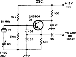
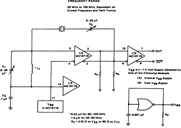
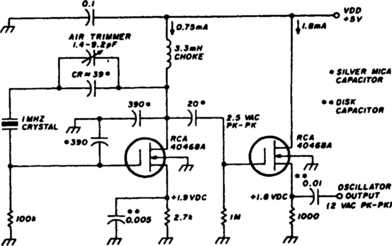
HIGH-FREQUENCY CRYSTAL OSCILLATOR
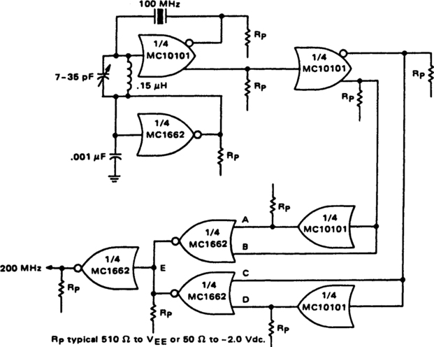
One section of the MC10101 is connected as a 100-MHz crystal oscillator with the crystal in series with the feedback loop. The LC tank circuit tunes the 100-MHz harmonic of the crystal and can be used to calibrate the circuit to the exact frequency. A second section of the MC10101 buffers the crystal oscillator and gives complementary 100-MHz signals. The frequency doubler consists of two MC10101 gates as phase shifters and two MC1662 NOR gates. For a 50% duty cycle at the output, the delay to the true and complement 100-MHz signals should be 90°. This can be built precisely with 2.5-ns delay lines for the 200-MHz output or approximated by the two MC10101 gates as shown.
96-MHz CRYSTAL OSCILLATOR
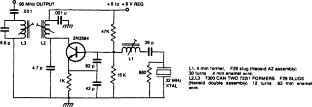
By using a crystal between 27.5 and 33 MHz, the 3rd harmonic will deliver between 82.5 and 99 MHz.
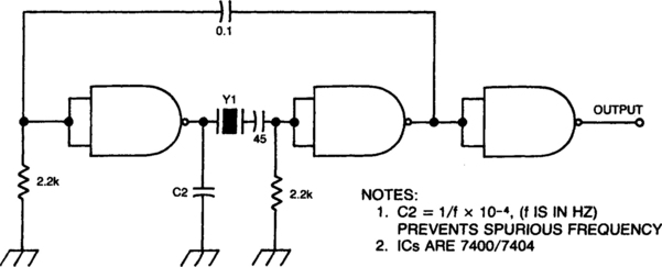
SIMPLE TTL CRYSTAL OSCILLATOR
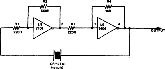
This simple and cheap crystal oscillator compasses one third of a 7404, four resistors and a crystal. The inverters are biased into their linear regions by R1 to R4, and the crystal provides the feedback. Oscillation can only occur at the crystal’s fundamental frequency.
BUTLER EMITTER-FOLLOWER OSCILLATOR (100 MHz)
This circuit has good performance without any parasitics because emitter-follower amplifier has a gain of only one with built-in negative feedback to stabilize its gain.
COLPITTS HARMONIC OSCILLATOR (BASIC CIRCUIT)
This circuit operates 30–200 ppm above series resonance. Physically simple, but analytically complex. It is inexpensive and has fair frequency stability.
COLPITTS HARMONIC OSCILLATOR (100 MHz)
L1C1 are selected to be resonant at a frequency below the desired crystal harmonic but above the crystal’s next lower odd harmonic. C2 should have a value of 30–70 pF, independent of the oscillation frequency. There is no requirement for any specific ratio of C1/C2, but practical harmonic circuits seem to work best when C1 is approximately 1 to 3 times the value of C2. Diodes D1, D2, D3 provide a simple regulated bias supply. The resistance of R1 should be as high as possible, because it affects the crystal’s in-circuit Q.
INTERNATIONAL CRYSTAL OF-1 LO OSCILLATOR
International Crystal OF-1 LO oscillator circuit for fundamental-node crystals.
CRYSTAL OSCILLATOR
This stable VXO using 6- or 8-MHz crystals uses a capacitor and an inductor to achieve frequency pulling on either side of series resonance.
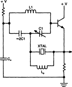
OVERTONE CRYSTAL OSCILLATOR
This design is for high reliability over a wide temperature range using fifth and seventh overtone crystals. The inductor in parallel with the crystal causes antiresonance of crystal C0 to minimize loading. This technique is commonly used with overtone crystals.
BUTLER APERIODIC OSCILLATOR
This circuit works well in the range of 50 to 500 kHz. Slight component modifications are needed for higher frequency operation. For operation over 3000 kHz, select a transistor that provides moderate gain (in the 60 to 150 range) at the frequency of operation and a gain-bandwidth product of at least 100 MHz.
PARALLEL-MODE APERIODIC CRYSTAL OSCILLATOR
The crystal is placed between the collector of the output stage and the base of the input stage. The frequency of oscillation can be set to a precise value with trimmer capacitor C1. The range of operation for this circuit is 500 kHz to 10 MHz. Extend the range downward (100 kHz) by increasing the value of C1 to 75 pF and by increasing the value of C2 to 22 pF.
VOLTAGE-CONTROLLED CRYSTAL OSCILLATOR
A voltage-variable capacitance tuning diode is placed in series with the crystal feedback path. Changing the voltage on VR varies the tuning diode capacitance and tunes the oscillator. The 510-kΩ resistor, R1, establishes a reference voltage for VR—ground is used in this example. A 100-kΩ resistor, R2, isolates the tuning voltage from the feedback loop and 0.1-µF capacitor C2 provides ac coupling to the tuning diode. The circuit operates over a tuning range of 0 to 25 V. It is possible to change the tuning range from 0 to 25 V by reversing the tuning diode D1. Center frequency is set with the 2–60 pF trimmer capacitor. Deviation on either side of center is a function of the crystal frequency. The table in Fig. 2-34 shows measured deviation in parts per million for several tested crystals.
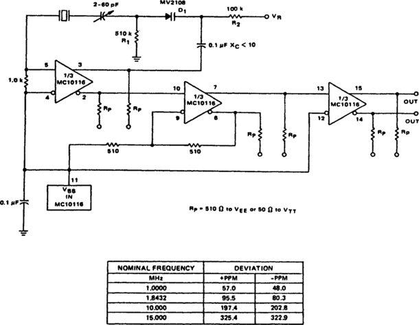
Fig. 2-34 Copyright of Motorola. Inc. Used by permission.
HIGH-FREQUENCY CRYSTAL OSCILLATOR
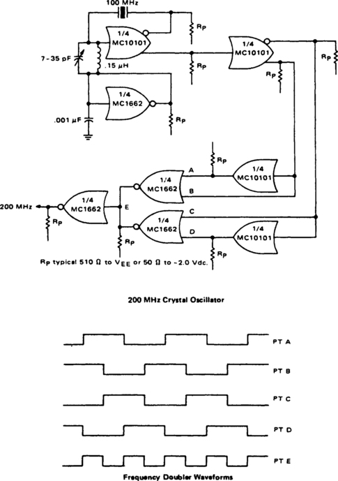
A high-speed oscillator is possible by combining an MECL 10-kΩ crystal oscillator with an MECL III frequency doubler, as shown. One section of the MC10101 is connected as a 100-MHz crystal oscillator with the crystal in series with the feedback loop. The LC tank circuit tunes the 100-MHz harmonic of the crystal and can be used to calibrate the circuit to the exact frequency. A second section of the MC10101 buffers the crystal oscillator and gives complementary 100-MHz signals. The frequency doubler consists of two MC10101 gates as phase shifters and two MC1662 NOR gates. For a 50% duty cycle at the output, the delay to the true and complement 100-MHz signals should be 90°. This can be built precisely with 2.5-ns delay lines for the 200-MHz output or it can be approximated by the two MC10101 gates. The gates are easier to incorporate and cause only a slight skew in output signal duty cycle. The MC1662 gates combine the 4-phase 100-MHz signals, as shown in Fig. B. The outputs of the MC1662’s are wire-OR connected to give the 200-MHz signal. MECL III gates are used because of the bandwidth required for 200-MHz signals. One of the remaining MC1662 gates is used as a VBB bias generator for the oscillator. By connecting the NOR output to the input, the circuit stays in the center of the logic swing or at VBB. A 0.001-µF capacitor ensures that the VBB circuit does not oscillate.
CRYSTAL-CONTROLLED OSCILLATOR OPERATES FROM ONE MERCURY CELL
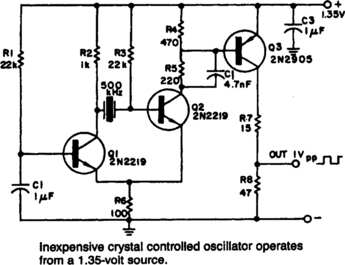
The circuit is powered by a single 1.35-V mercury cell and it provides a 1-V square-wave output. As shown, the crystal is a tuned circuit between transistors Q1 and Q2, which are connected in the common-emitter configuration. Positive feedback, provided by means of R, permits oscillation. The signal at the collector of Q2 is squared by Q3, which switches between cutoff and saturation. R7 permits short-circuit-proof operation.
COLPITTS OSCILLATOR
Bias for the pnp bipolar transistor is provided by resistor voltage-divider network R1/R2. The collector of the oscillator transistor is kept at ac ground by capacitor C5, placed close to the transistor. Feedback is provided by capacitor voltage divider C2/C3.
LOW-FREQUENCY CRYSTAL OSCILLATOR—10 to 150 kHz
C1 in series with the crystal, can be used to adjust the oscillator output frequency. The value can range between 20 pF and 0.01 µF, or it can be a trimmer capacitor and that will approximately equal the crystal load capacitance. X values are approximate and can vary for most circuits and frequencies; this is also true for resistance values. Adequate power supply decoupling is required; local decoupling capacitors near the oscillator are recommended. All leads should be extremely short in high-frequency circuits.
OVERTONE CRYSTAL OSCILLATOR
This oscillator is designed for overtone crystals in the 20–100 MHz range operating in the third and fifth mode. Operating frequency is determined by the tuned circuit.
IC-COMPATIBLE CRYSTAL OSCILLATOR
Resistors R1 and R2 temperature-stabilize the NAND gates; they also ensure that the gates are in a linear region for starting. Capacitor C1 is a dc block; it must have less than 1/10-Ω impedance at the operating frequency. The crystal runs in a series-resonant mode. Its series resistance must be low; AT-cut crystals for the 1- to 10-MHz range work well. The output waveshape has nearly a 50% duty cycle, with chip-limited rise times. The circuit starts well from 0° to 70°C.
CRYSTAL OSCILLATOR PROVIDES LOW NOISE
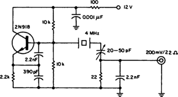
The oscillator delivers an output of high spectral purity without any substantial sacrifice of the usual stability of a crystal oscillator. The crystal in addition to determining the oscillator’s frequency, is used also as a low-pass filter for the unwanted harmonics and as a bandpass filter for the sideband noise. The noise bandwidth is limited to less than 100 Hz. All higher harmonics are substantially suppressed—60 dB down for the third harmonic of the 4-MHz fundamental oscillator frequency.
DISCRETE SEQUENCE OSCILLATOR
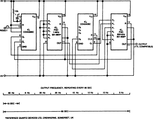
The swept-frequency oscillator offers an inexpensive source of discrete frequencies for use in testing digital circuits. In this configuration, the circuit generates an 80-second sequence of eight frequencies, dwelling for 10 seconds on each frequency. You can change the dwell time or the number of frequencies. Frequencies can range from 0.005 Hz to 1 MHz.
The programmable crystal oscillators, PXOs, IC2 and IC4 can each generate 57 frequencies in response to an 8-bit external code. IC2 contains a 1-MHz crystal and produces a 0.05-Hz output. IC4 contains a 600-kHz crystal; its output changes in response to the combined outputs of the 12-stage binary counter IC3 (Q1 and Q2) and the PXO IC2.
To generate more frequencies, you can use one or more of IC3’s outputs, (Q3, Q4, Q5) to drive one or more of IC4’s inputs (P4, P5, P6). Similarly, you can rewire IC2 or drive it with other logic to control the duration of each frequency. IC1, a monostable multivibrator, provides a system reset. It initiates the sequence shown, beginning at 60 Hz, in response to a positive pulse.
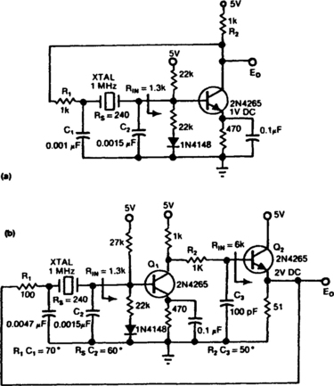
1-MHz PIERCE OSCILLATORS
Simple network design is a key feature of the Pierce circuit, as these 1-MHz oscillators illustrate. Operating the crystal slightly above resonance (Fig. 2-44a) requires only one high-gain transistor stage. Operating it exactly at series resonance (Fig. 2-44b) requires an extra RC phase lag and two transistors which can have lower gain.
SIMPLE CMOS CRYSTAL OSCILLATOR
The circuit is an inverter set up as a linear amplifier. Adding the crystal and capacitors to the feedback path, we turn the amplifier into an oscillator and force it to oscillate at, or least very near, the crystal’s resonant frequency. Trimmer capacitor C2 adjusts the actual operating frequency of the circuit. The crystal should be a parallel-resonant type; maximum frequency will depend partly on supply voltage, but it should be possible to go to at least 1 MHz.
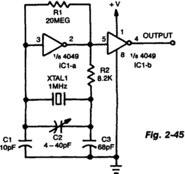
Fig. 2-45 Reprinted with permission from Radio-Electronics Magazine February 1987. Copyright Gernsback Publications, Inc., 1987.
CRYSTAL TIMEBASE
An on-board oscillator and a 17-stage divider compose IC1. By connecting a standard 3.58-MHz, television color-burst crystal as shown, an accurate source of 60-Hz squarewaves is generated at the IC’s output, pin 1. Those pulses are then fed to IC2, a 4024 seven-stage ripple counter. Its outputs are connected to different gates in IC3, which is a dual four-input NAND gate. Depending on which position pulse-select switch S2 is on, one of those gates will provide an output/reset pulse of the selected width.
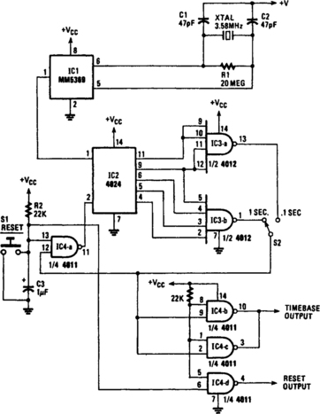
Fig. 2-46 Reprinted with permission from Radio-Electronics Magazine, February 1986. Copyright Gernsback Publications, Inc., 1986.
LOW-FREQUENCY PIERCE OSCILLATOR
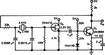
The Pierce circuit oscillates at 4 kHz. At low frequencies, the crystal’s internal series resistance Rs is quite high (45 K at 4 kHz). Therefore, an FET-based source follower is included to prevent Q1 from loading the crystal output.
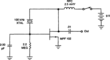
1-MHz FET CRYSTAL OSCILLATOR
This stable oscillator circuit exhibits less than 1-Hz frequency change over a VDD range of 3–9 volts. Stability is attributed to the use of MOSFET devices and the use of stable capacitors.
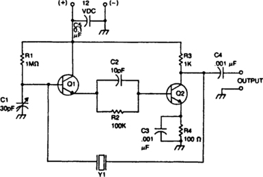
PIERCE CRYSTAL OSCILLATOR
The JFET Pierce oscillator is stable and simple. It can be the clock of a microprocessor, a digital timepiece, or a calculator. With a probe at the output, it can be used as a precise injection oscillator for troubleshooting. Attach a small length of wire at the output and this circuit becomes a micropower transmitter.
OVERTONE OSCILLATOR WITH CRYSTAL SWITCHING
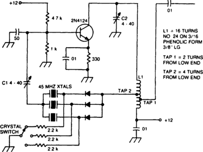
The large inductive phase shift of L1 is compensated for by C1. Overtone crystals have very narrow bandwidth; therefore, the trimmer has a smaller effect than for fundamental-mode operation.
CRYSTAL OSCILLATOR
The crystal is in a feedback circuit from collector to base. A trimmer capacitor in series shifts the point on the reactance curve where the crystal operates, thus providing a frequency trim. The capacitor has a negative reactance so that the crystal is shifted to operate in the positive reactance region.
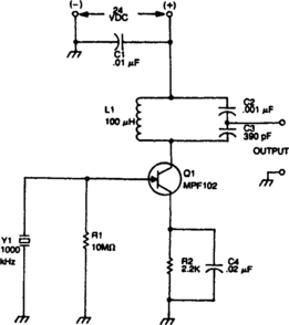
FIFTH-OVERTONE OSCILLATOR
This circuit isolates the crystal from the dc base supply with an rf choke for better starting characteristics.
CRYSTAL-CONTROLLED BUTLER OSCILLATOR
A typical Butler oscillator (20–100 MHz) uses an FET in the second stage; the circuit is not reliable with two bipolars. Sometimes two FETs are used. Frequency is determined by LC values.
SCHMITT TRIGGER CRYSTAL OSCILLATOR
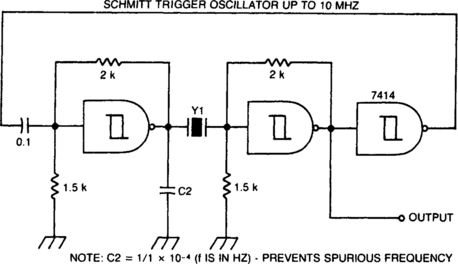
A Schmitt trigger provides good squaring of the output, and sometimes eliminates the need for an extra output stage.
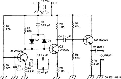
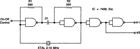
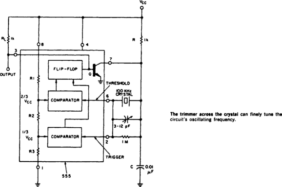
PRECISION CLOCK GENERATOR
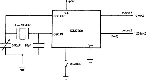
The CMOS IC directly drives 5 TTL loads from either of 2 buffered outputs. The device operates to 10 MHz and is bipolar, MOS, and CMOS compatible.
MILLER OSCILLATOR (CRYSTAL CONTROLLED)
The drain of the JFET Miller oscillator is tuned to the resonant frequency of the crystal by an LC tank circuit.
BUTLER EMITTER-FOLLOWER OSCILLATOR (BASIC CIRCUIT)
This circuit operates at or near series resonance. It is a good circuit design with no parasitics. It is easy to tune with good frequency stability.
BUTLER COMMON-BASE OSCILLATOR (BASIC CIRCUIT)
This circuit operates at or near series resonance. It has fair to poor circuit design with parasitics, touch to tune, and fair frequency stability.
PIERCE HARMONIC OSCILLATOR (100 MHz)
The output resistance of the transistor’s collector, together with the effective value of C1, provides an RC phase lag of 30–50°. The crystal normally oscillates slightly above series resonance, where it is both resistive and inductive. Above series resonance, the crystal’s internal impedance (resistive and inductive) together with C2 provides an RLC phase lag of 130–150°. The transistor inverts the signal, providing a total of 360° of phase shift around the loop. Inductor L1 is selected to resonate with C1 at a frequency between the crystal’s desired harmonic and its next lower odd harmonic. Inductor L1 offsets part of the negative reactance of C1 at the oscillation frequency.
INTERNATIONAL CRYSTAL OF-1 HI OSCILLATOR
International Crystal OF-1 HI oscillator circuit for third-overtone crystals. The circuit does not require inductors.
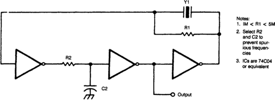
TTL-COMPATIBLE CRYSTAL OSCILLATOR
Adjust R1 for about 2 volts at the output of the first gate. Adjust C1 for best output.
THIRD-OVERTONE CRYSTAL OSCILLATOR
This circuit uses a 74S00 Schottky TTL gate; no inductors are required.
CRYSTAL CHECKER
This circuit is a simple Pierce oscillator with an LED go/no go display. The checker works best with crystals having fundamental frequencies in the 7 to 8 MHz range.
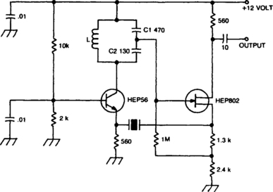
CRYSTAL OSCILLATOR/DOUBLER
The crystal operates into a complex load at series resonance. L1, C1, and C2 balance the crystal at zero reactance. Capacitor C1 fine-tunes the center frequency. Tank circuit L2/C3 doubles the output frequency. The circuit operates as an FM oscillator-doubler.
VARACTOR-TUNED 10-MHz CERAMIC RESONATOR OSCILLATOR
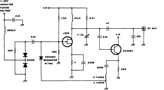
The FET input amplifier has fixed bias with source feedback. This provides a very high input impedance with very low capacitance. The FET amplifier drives an emitter follower, which, in spite of the fact that it has a low output impedance, feeds a transformer with a 3:1 turns ratio for a nine-fold impedance reduction. The result is an impedance at the ceramic resonator of a few ohms maximum. The varactor-tuned ceramic resonator oscillator has a significant frequency-temperature coefficient. The tuning range of the VCO is approximately 232 kHz, with a temperature coefficient of 350 Hz per degree centigrade. When using this circuit as a VCO, the entire 232-kHz range cannot be used because some of the tuning range must be sacrificed for the temperature dependence. If the required tuning range was 200 kHz (leaving 32 kHz for temperature variation), the resulting temperature variation would be more than 90°C.
10-MHz CRYSTAL OSCILLATOR
This crystal oscillator is a FET equivalent of a vacuum tube tuned to plate-tuned grid crystal oscillator. Feedback is via the drain to gate capacitance.
PIERCE HARMONIC OSCILLATOR (BASIC CIRCUIT)
This circuit operates 10–40 ppm above series resonance. It is a good circuit design with good to very good frequency stability.
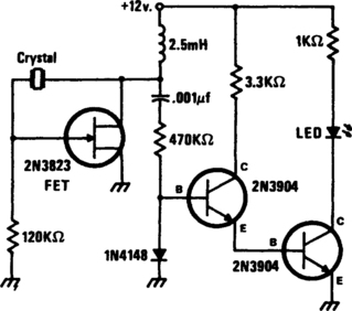
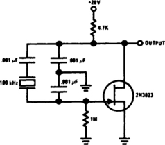
STABLE LOW-FREQUENCY CRYSTAL OSCILLATOR
This Colpitts-crystal oscillator is ideal for low-frequency crystal oscillator circuits. Excellent stability is assured because the 2N3823 JFET circuit loading does not vary with temperature.
JFET PIERCE CRYSTAL OSCILLATOR
The JFET Pierce crystal oscillator allows a wide frequency range of crystals to be used without circuit modification. Because the JFET gate does not load the crystal, good Q is maintained, thus ensuring good frequency stability.
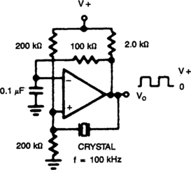
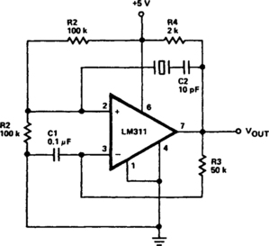
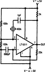
CRYSTAL OSCILLATOR
This circuit uses an LT1011 comparator biased in its linear mode and a crystal to establish its resonant frequency. This circuit can achieve a few hundred kHz, and it has temperature independent clock frequency with nearly 50% duty cycle.
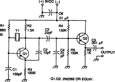
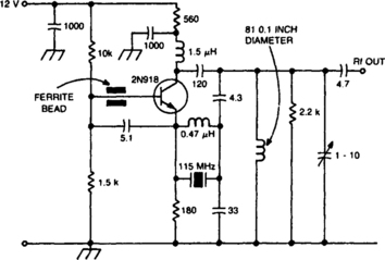
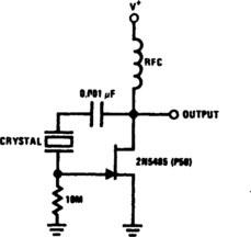
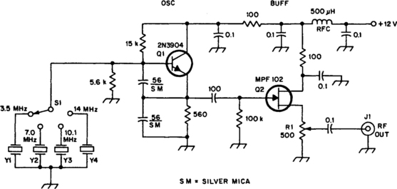
CRYSTAL-CONTROLLED SIGNAL SOURCE
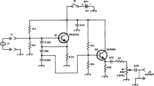
This general-purpose signal source serves very well in signal-tracing applications. The output level is variable to more than 1 Vrms into a 50-Ω load. Almost any crystal in the 1- to 15-MHz range can be used. Q1 forms a Colpitts oscillator with the output taken from the emitter. A capacitive voltage divider (across the 2.2-kΩ emitter resistor) reduces the voltage applied to the buffer amplifier, Q2. The buffer and emitter follower, provides the low-input impedance necessary to drive 50-Ω loads.
HIGH-FREQUENCY SIGNAL GENERATOR
A switched-crystal Colpitts oscillator is used at Q1 to provide four tuning ranges from 1.7 to 3.1 MHz, 3.0 to 5.6 MHz, 5.0 to 12 MHz and 11.5 to 31 MHz. A Zener diode (D2) is used at Q1 to lower the operating voltage of the oscillator. A small-value capacitor is used at C5 to ensure light coupling to the tuned circuit. Q2 is a source-follower buffer stage. It helps to isolate the oscillator from the generator-output load. The source of Q2 is broadly tuned by means of RFC1. Energy from Q2 is routed to a fed-back, broadband class-A amplifier. A 2-dB attenuator is used at the output of T1 to provide a 50-0 termination for Q3 and to set the generator-output impedance at 50 Ω. C16, C17 and RFC2 form a brute-force RF decoupling network to keep the generator energy from radiating outside the box on the 12-V supply.
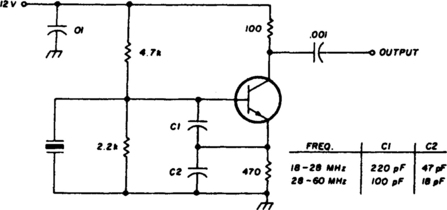
50-MHz VHF CRYSTAL OSCILLATOR
Figure 2-82 shows a 50-MHz oscillator operating on a third harmonic. The collector’s load resistor R1 has been increased because the quartz crystal’s internal series resistance Rs increases with frequency in the VHF range. The crystal’s internal series resistance, Rs, is 30 Ω, and the transistor’s minimum current gain HFE is 100. Using the same technique as for the 20-MHz oscillator, the external series RLCL equivalent load seen by the 50-MHz crystal is 5.6 Ω (RL) and 1000 pF (CL).
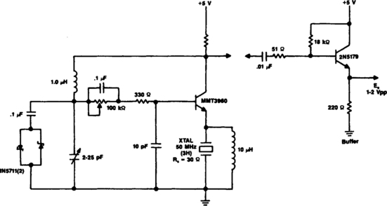
Fig. 2-82 R. Matthys. RF Dealgn, March 1987. p. 31.