
Photoelectrochemical cells for hydrogen generation
Abstract:
This chapter discusses the generation of hydrogen in photoelectrochemical cells. Initially, the fundamental aspects of photoelectrolysis (principles, energetics and kinetics) and efficiency considerations will be considered. The chapter then devotes attention to materials issues and challenges. The final section deals with emerging frontiers and future directions.
5.1 Introduction
It has long been accepted that world demand for energy will increase steadily for the foreseeable future. Nevertheless, the general view until the end of the last century was that intensive exploitation of conventional resources was capable of providing an adequate supply of energy. Today the situation has changed entirely, and everyone from law-makers to the general population understands the urgency of responding to the threat of depletion of fossil fuels. At the same time, we are experiencing the rapid rise of energy costs and witness the direct evidence of the environmental impact associated with the prolonged release of greenhouse gases generated by combustion of fossil fuels. Recent catastrophic events such as the Gulf of Mexico oil spill and the Fukushima nuclear accident seem to have significantly changed the thinking of influential policymakers around the world. This was evident from the recent decision to close down all nuclear reactors in Germany. Studies of known carbon-free renewable energy sources have been intensified, and their viability to provide alternative energy is being evaluated. Meanwhile, the search for new energy-harvesting methods has also taken a new lease of life. Due to the renewed interest and intensive research and development on its use as an alternative energy vector, hydrogen is poised to become the nuclear-free, clean and non-fossil fuel of tomorrow, provided that it can be generated at a low cost as well as stored and transported safely. It has the highest mass energy density (high heat value ~ 141.78 MJ/kg, low heat value ~ 120 MJ/kg at 25°C), almost 2.5 times the energy released during the combustion of conventional hydrocarbon fuels (Lide, 1994; Rand and Dell, 2007). Given this scenario, it is very surprising that at present merely a 0.05% of global primary energy supply is met by solar energy harvesting methods, and the enormous potential of solar energy remains largely untapped (Grätzel, 1989; Wijayantha and Auty, 2005; Solangi et al., 2011). Sunlight and water are the two widely abundant resources on Earth. Realizing a low-cost route to convert sunlight to hydrogen by splitting water is one of the most secure ways of guaranteeing a solution for the world energy demand for many generations to come. The concept of using photovoltaic (PV) energy for production of hydrogen has been considered since the discovery of silicon PVs, but the practical use of solar cells coupled to electrolyzers to gen- erate hydrogen on an industrial scale is currently held back by the cost of PVs and by other scientific and technological challenges associated with it (i.e., power mismatch between the PV cells and electrolyzer caused by deg- radation of PV cells) (Tributsch, 2008). The outcome of ambitious international collaborative projects such as HYSOLAR has shown the economic, scientific and technological concerns of that approach (Siegel and Schott, 1988; Steeb et al., 1988; Tributsch, 2008). Direct photoelectrochemical water splitting (or photoelectrolysis) is an alternative approach, and the devel- opment of this concept has continued since the seminal work of Fujishima and Honda (1972). Advances made in fuel cell technology and direct com- bustion engines have further increased the demand for the development of low-cost hydrogen generation technologies including photoelectrolysis. This chapter discusses fundamental aspects of photoelectrolysis (principles, energetics and kinetics), efficiency considerations, materials, issues and chal- lenges, emerging frontiers and future directions.
5.2 Photoelectrochemical cells: principles and energetics
Our understanding of semiconductor photoelectrochemistry today is based on the pioneering work conducted by Gerischer, Pleskov, Memming and others (Gerischer, 1977; Memming, 1978; Nozik, 1980; Albery, 1982; Lewis, 1984; Peter, 1990; Pleskov, 1990). Since this early work, the area has pro- gressed significantly. The term photoelectrochemical (PEC) generally refers to an electrochemical process that is caused by light. As the name implies, anodic or cathodic processes (or both) can be driven by light in a PEC cell. When the overall process taking place in a PEC cell is thermodynam- ically uphill (positive ΔG), it is called a photosynthetic cell. Conversely, if the process is thermodynamically downhill (negative ΔG), it is referred to as a photocatalytic cell. Photoelectrolysis and photo-induced metal reduction on semiconductor surface coupled to a complementary oxidation are typical examples of the former and latter (Tennakone and Wijayantha, 1998; Rajeshwar, 2007).
The potential for the conversion of solar energy to electricity or fuels at the semiconductor/electrolyte junction led to widespread interest in the 1970s which was initially sparked by the oil crisis (Peter, 1999). The 1980s witnessed a burgeoning interest in the development of regenerative PEC cells based on redox electrolytes, but stability and cost proved to be the main barriers that prevented industrial-scale investment. The development of regenerative dye-sensitized nanocrystalline TiO2 PEC cells (DSCs) with impressive power conversion efficiency in the early 1990s by Gratzel and co-workers was a major breakthrough (O'Regan and Grätzel, 1991). This led to a flurry of activities and investments from governments and industry around the world. This renewed interest in regenerative PEC cells revi- talized semiconductor photoelectrochemistry, including photoelectrolysis, which in recent years has benefited from advances made in DSCs as well as in nanotechnology (e.g., development of nanostructured semiconductor electrodes).
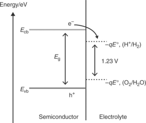
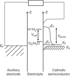
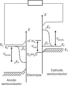
In order for hydrogen evolution reaction (HER) and oxygen evolu- tion reaction (OER) to occur at an illuminated semiconductor/electrolyte interface, the energies of the bottom of the conduction band and the top of the valence band are required to be appropriately aligned with respect to the electrochemical potentials of H+/H2and O2/H2O couples (Nozik and Memming, 1996). Figure 5.1 illustrates an ideal energy scheme, in which the photogenerated electrons and holes can take part in the HER and OER reactions if they survive recombination and arrive safely at the semicon- ductor/electrolyte interface. The minimum energy required to split one molecule of water (to one molecule of H2 and half a molecule of oxygen) under standard conditions is 2.46 eV, as implied in Fig. 5.1. However, HER and OER occurring at illuminated semiconductor/electrolyte interfaces are associated with overpotentials, and practical devices require about 1.6–2.4 eV to split water (Turner, 1999; Walter et al., 2010; Chou et al., 2011). The voltage required to drive a particular reaction relative to the redox potential of that reaction at an identical condition is referred to as the overpotential. If the HER and OER occur in nearby sites on the semiconductor surface, the overall energy conversion efficiency is likely to be very inefficient as the products may react with each other, dissipating heat (Gerischer, 1977).
Separation of photogenerated electron–hole pairs takes place within the space charge region, and minority carriers (holes for n-type semiconductors and electrons for p-type semiconductors) are driven to the electrolyte interface, where they react to form oxygen in the case of holes and hydrogen in the case of electrons. Majority carriers move to the counter electrode where they take part in the other half-cell reaction to complete the photoelectroly- sis process. The photoelectrolysis cell therefore offers a simple way to separate the photo-induced water oxidation and reduction reactions in separate compartments, allowing hydrogen to be harvested in the absence of oxygen.
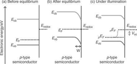
The bulk electronic properties of an extrinsic semiconductor are determined by doping density of the material. As shown in Figs 5.2a and 5.3a, respectively, the position of the Fermi level (before the electrode comes in to contact with an electrolyte) is related to the n-type or p-type characteristics of the semiconductor. For non-degenerate semiconductors, the electron and hole densities in the conduction and valence bands are related to the Fermi energy EF and to the effective densities of states in the conduction and valence bands as
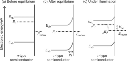
5.2 The band energetics at anodic semiconductor/electrolyte interface (a) before equilibrium, (b) after equilibrium and (c) under illumination.
5.3 The band energetics at cathodic semiconductor/electrolyte interface (a) before equilibrium, (b) after equilibrium and (c) under illumination.
where no and po are the electron and hole densities, respectively, and Nc and Nv are the corresponding effective densities of states in the conduction and valence bands. The Fermi level is the electrochemical potential is the electrochemical potential of electrons in a semiconductor. The product of the electron and hole densities can be described by the following relation, where Eg is the band gap energy:
The energetics of the semiconductor/electrolyte interface have been well documented (Morrison, 1980; Peter, 1999; Pierret, 2003; Sze and Ng, 2007; Archer and Nozik, 2008; Würfel, 2009; Walter et al., 2010). When a bulk semiconductor photoanode or photocathode is brought into contact with a liquid electrolyte containing donor and acceptor species, electrons will flow from the phase which has the highest electrochemical potential to the other phase, until electronic equilibrium is established (the electrochemical potential of the redox couple is equivalent to the redox Fermi level in the electrolyte). This charge transfer leads to the build up of an interfacial electric field. The corresponding 'contact potential' is equivalent to the initial difference in electrochemical potential between the two phases. Figure 5.2b shows this situation for an anodic semiconductor in contact with a liquid electrolyte containing donors A− and acceptors, A. As the electrochemical potential of the donor/acceptor couple is more negative than that of the semiconduc- tor, the electrode has an excess positive charge (i.e., ionized donor atoms) which will be balanced by excess negative charge in the liquid electrolyte. This situation results in a parabolic potential drop across the space charge region leading to the well-known band bending at the semiconductor/electrolyte interface. Under these depletion conditions, the potential drop occurs mostly in the space charge region unless the donor density is very high. The positive charge in the semiconductor is spread across the space charge width, whereas the negative charge is confined to a much narrow region called the Helmholtz layer in the electrolyte. The space charge layer width W is given by
Here, ΔϕSC is potential drop across the space charge region, ε is the rel- ative permittivity of semiconductor,ε0 is the permittivity of free space and Nd is the donor density. As indicated by Equation [5.4] r the width of this space charge region depends on the doping density of the semiconductor. For example, it can be as large as 1 μm for a semiconductor with a doping density of 1021 m-3. A p-type semiconductor in contact with an electrolyte behaves in an analogous manner, as illustrated in Fig. 5.3b. The nEF and pEF in Figs 5.2c and 5.3c represent the electron quasi-Fermi level and hole quasi- Fermi level (non-equilibrium electron and hole populations, respectively, under steady-state illumination).
When electron–hole pairs are generated by light absorption inside the space charge region, they are separated by the gradients of Fermi levels as shown in the earlier figures. The electron–hole pairs generated at the interior of the semiconductor electrode beyond the space charge layer may also be separated if the minority carrier diffusion length is sufficiently large. As a rule of thumb, if the electrochemical potential difference between the semiconductor and electrolyte before attaining the equilibrium is of the order of 1 eV, the depletion width for a moderately doped semiconductor can be a few hundred nanometres and the associated electric field can be as large as 105 V cm-1 on the surface (it varies with the distance in the interior of the semiconductor electrode). As the typical charge carrier mobility for crystalline semiconductors is of the order of 10–103 cm2 V−1 s−1, the electron- hole pair generated inside the space charge region may be easily separated. The minority carriers travel to the surface under the electric field and then undergo interfacial reactions whilst the majority carriers transport to the interior of the semiconductor electrode and then transfer to the auxiliary electrode via an external circuit. However, in reality the situation may be different as slow electron transfer rate at the semiconductor surface may lead to minority carrier build-up at the interface, altering the quasi-Fermi level profile and band bending.
As shown in Fig. 5.2c, when an anodic semiconductor/electrolyte interface is under illumination (non-equilibrium condition), the electron density can be described by the following relation:
Similarly, the hole density of a cathodic semiconductor/electrolyte interface under illumination is given by
Therefore, the electron and hole densities under illumination (non- equilibrium) can be related to the densities under dark equilibrium condition as
For example in the case of an n-type semiconductor photoanode, if the minority career holes undergo interfacial reactions with electron donors in the electrolyte, negative charge is accumulated in the semiconductor leading to a photovoltage under open-circuit conditions. This can be understood by considering the change of interfacial energetics that may take place at anodic semiconductor/electrolyte interface from dark-equilibrium to illuminated non-equilibrium condition (see the difference in interfacial energetics between Fig. 5.2b and 5.2c). The analogous situation for a p-type photocathode semiconductor/electrolyte interface can also be understood by comparing Fig. 5.3b and 5.3c. The Gibbs energy change driving interfacial electron transfer during water photo-oxidation (photocurrent) is determined by the energy difference between the quasi-Fermi level of holes (pEF) in the semiconductor and the redox energy level corresponding to the oxygen reduction potential.
Equation [5.7] shows that the free energy available at the semiconductor/electrolyte interface is given by the difference between electron and hole quasi-Fermi levels under illumination. However, in general, the magnitude of attainable photovoltage is determined by the energetic alignments at the interface whereas the magnitude of the photocurrent is determined by a number of kinetic loss mechanisms that may occur in a PEC cell in the pho- tostationary state. These include charge recombination at the interface, in the bulk and within the space charge region, tunnelling through the electric potential barrier near the surface, and thermally surmounting the interfacial potential barrier that may restrict attainable photovoltage and photocurrent. There are many parameters that determine the kinetics of each process (i.e., semiconductor material properties, the kinetics of electrolyte). Sometimes all loss mechanisms except the rate of fundamentally limiting one (typically, the bulk recombination) can be suppressed, so that such systems may oper- ate at their maximum attainable efficiency limit under the photostationary condition providing the optimum photovoltage and photocurrent (Lewis, 2005). Defect-rich semiconductors hardly show a photoeffect.
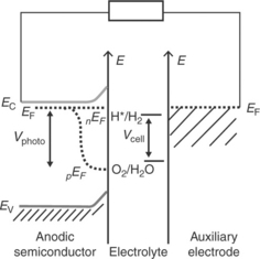
The energetics of a photoanodic semiconductor/electrolyte interface with respect to the water redox potentials H+/H2 and O2/H2O are illustrated in Fig. 5.4 assuming that there are no interfacial reactions. The anode is con- nected to an auxiliary cathode (which is dipped in the same electrolyte) via an external circuit. In this case, it is assumed that the band energetics of the semiconductor is favourable to drive the water oxidation and reduction reactions by photogenerated holes and electrons at the semiconductor/electrolyte interface and the auxiliary electrode/electrolyte interface, respectively. The energetics of analogous cathodic semiconductor/electrolyte interface with respect to the water redox potentials are shown in Fig. 5.5. As discussed in Section 5.4, semiconductor materials that provide desira- ble interfacial energetics for unassisted photoelectrolysis are not currently available. Efforts have been made to overcome this limitation by construct- ing dual band gap photoelectrodes by combining smaller band gap sem- iconductor materials that have complementary energetic, light harvesting and stability characteristics under device operation condition (Bolton et al, 1985; Nozik, 1996; Khaselev et al, 2001). However, a detailed discussion of such dual band gap photoelectrodes and photocatalysis cells associated with them is beyond the scope of this chapter.
5.3 Photoelectrochemical cell configurations and efficiency considerations
5.3.1 Theoretical considerations
Identifying the factors that determine the overall solar energy conversion efficiency is critically important in evaluating the overall cost benefit of the PEC water-splitting process. The key commercial decisions (i.e., longterm investment on research and development) are always associated with device efficiency, fabrication cost, material availability/scarcity and others. The conversion of solar energy into useful forms can be classified into thermal and photonic in general. Solar thermal processes are determined by the Carnot efficiency whereas solar photonic processes are limited by fundamental considerations of optical excitation at molecular level (for organic light harvesters) and/or bandgap excitation (for inorganic light harvesters).
Shockley and Queisser presented the concept of ideal photovoltaic cell (for a p-n junction) and showed that the maximum conversion efficiency is 31% under AM 0 illumination (Shockley and Queisser, 1961). Ross and Kelvin generalized the Shockley and Queisser treatment to all photochemical energy conversion systems (Ross and Calvin, 1967). Taking into account Ross and Calvin treatment further, Bolton and co-workers considered solar photonic converter configurations and limiting efficien- cies (Bolton, 1978, 1996; Bolton et al., 1985). A few recent papers have also discussed PEC cell configurations in terms of overall solar to hydro- gen conversion efficiency (Rajeshwar, 2007; Chen et al, 2010; Walter et al, 2010). The efficiency (η) of conversion of incident solar energy to chemical (Gibbs) energy is given by
where J is the absorbed photon flux (photons s−1 m−2,μex is the excess chemical potential generated by light absorption, ϕconv is the quantum yield for absorbed photons to chemical product generation, and S is the total incident solar irradiance in Wm−2. ϕconv is a function of light harvesting, charge transport, charge collection and interfacial charge transfer efficiencies.
Bolton's classification is based on the number of photosystems (i.e., S for a single photosystem and D for dual photosystems) employed in each device configuration by considering a different light absorption threshold for each photosystem. The scheme classification is generalized by taking into account the minimum number of photons required to generate solar production of any reduced fuel by taking the minimum number of photons required to generate reducing equivalent of one molecule of hydrogen. If the device is designed based on a single semiconductor material with a band gap of 1.6 eV (light absorption threshold ~ 775 nm), the maximum solar energy conversion efficiency under standard AM1.5 illumination (assuming that hydrogen evolution takes place under standard conditions) is 30.7% (Bolton et al., 1985). The calculation considers that the device only needs two photons to generate one molecule of hydrogen (S2). However, if the device requires four photons to produce one mole of hydrogen (S4), the ideal maximum solar energy conversion efficiency under standard AM1.5 illumination would be 30.6%. Similarly, the terms D2 and D4 are assigned for devices that utilize dual photosystems (Bolton et al, 1985).
5.3.2 Experimentally assessing the solar to hydrogen conversion efficiency
The energy conversion efficiency of practical devices is significantly lower than the theoretical maximum conversion efficiency due to a number of energy losses occurring in real devices under operational conditions. Hence, all energy losses need to be accounted for in order to estimate the practically attainable efficiency for a given device configuration that utilizes a particular material combination and a specific illumination profile. Nonradiative recombination and loss occurring due to overpotentials (that are required to drive the OER and HER) are some of the losses in real devices under operational conditions. The next section deals with the determination of solar energy conversion efficiency of practical photoelectrolysis cells.
In terms of solar energy conversion efficiency of practical PEC water- splitting systems, the published literature to date generally deals with (i) mainstream reporting (bench marking efficiency), (ii) specific material performance reporting (diagnostic efficiency), (iii) fundamental aspects report- ing (charge generation, transfer, collection, interfacial charge transfer and mechanistic aspects that limit the efficiency) and new device configurations reporting (introducing new device structures to maximize the overall efficiency) (Chen et al., 2010). A detailed discussion on different PEC water- splitting cell configurations/systems and the solar to hydrogen conversion efficiency will not be attempted here as it is beyond the scope of this chapter. Instead, a brief outline of methods of experimentally assessing the solar to hydrogen conversion efficiency is presented below. Recent reports have highlighted the necessity of the correct measurement conditions in order to determine the solar-to-hydrogen conversion efficiency accurately. Generally, there are two ways of determining the overall solar-to-hydrogen conversion efficiency of PEC water-splitting systems practically. In the first method, it is calculated by taking into account the rate of hydrogen generation (Equation [5.9]). In the second method, the efficiency is determined by taking into consideration the short-circuit photocurrent density (Equation [5.10]). In order to do that the device is illuminated with Air Mass 1.5 Global (AM 1.5 G) spectra. Often the device is in two-electrode configuration where OER and HER take place in each electrode only under illumination and no external voltage is applied. Two electrodes immersed in the aqueous elec- trolyte are required to be separated by a proton exchange membrane in order to facilitate the ionic transport across (i.e., no pH gradient between anodic and cathodic side) and to prevent the exothermic reaction between the overall reaction products, oxygen and hydrogen. Connection of the two electrodes externally makes it possible to record the photocurrent density. Knowing the rate of hydrogen generation, the solar-to-hydrogen conversion efficiency (η) can be determined by the relation
where the [rH2 ] is the rate of hydrogen generation in mol/s, ΔG is the Gibbs free energy change for the generation of one mole of H2 by splitting water under standard conditions (237.2 kJ/mol), P is the power density of illumi- nation intensity in W/m2 and A is the illuminated area of the electrode. It is generally expected that the rate of hydrogen generation at the cathode (or photocathode) is twice the rate of oxygen generation at the anodic (or photoanode) (i.e., the Faradaic efficiency of the overall process is 100%). This can be verified by conducting a quantitative analysis of gas generated at each electrode (i.e., by determining the gas type and rate of evolution). Recording the photocurrent in the external circuit allows determination of the solar-to-hydrogen conversion efficiency by using
where the Jsc is the photocurrent density in A/m2 and P is the power density of illumination intensity in W/m2. (In some reports, an extra term (ηF) is incorporated in Equation [5.9] in order to compensate the losses if HER and/or OER are not 100% Faradaic. However, the ηF may not be constant as the HER and OER progress when the cell operates, due to accumulation of undesirable products as reaction intermediates undergo side reactions in cathodic/anodic or both electrodes.) When using Equation [5.10], it is important to establish that the recorded photocurrent density corresponds to the generation of hydrogen and oxygen in cathode and anode, respec- tively (i.e., Faradaic efficiency of both HER and OER are 100%).
Stable semiconductor materials with desirable band energy positions are not currently available that would allow the design of PEC water-splitting devices that can operate without an external bias. Due to this situation, many device configurations reported to date use an externally applied voltage to assist the overall water-splitting process (Walter et al, 2010). In some cases, an internal chemical bias has been generated by employing electrolyte solutions with an appropriate pH gradient between the anode and cathode com- partments of the cell, in order to achieve the same objective (Fujishima and Honda, 1972; Aspnes and Heller, 1983). The overall efficiency of such systems needs to be evaluated with extra care as the HER and OER dynamics may alter the pH difference between the cathode and anode compartments when the device operates. As for devices that operate under an external applied voltage, the magnitude of the required voltage depends on the band energy positions in the electrolyte concerned. Equation [5.11] provides a convenient way of calculating the efficiency of PEC water-splitting devices under condi- tions of applied bias. It is clear from this equation that the externally applied voltage (Vapp) cannot exceed 1.23 V under standard operational conditions if the PEC water-splitting cell is to have a non-zero efficiency:
where J is the external photocurrent density in A/m2, P is the power density of illumination intensity in W/m2. In this case, it is assumed that the Faradaic efficiency for water splitting is 100%.
5.4 Semiconductor photoanodes: material challenges
5.4.1 Introduction to materials challenges
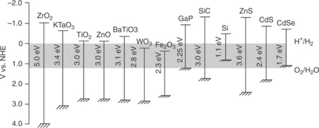
Photoelectrolysis cells require semiconductor materials that harvest sun- light efficiently and sustain the water-splitting reactions under illumination without external assistance (bias voltage) for prolonged periods at a fast enough rate without substantial kinetic losses. Hence, semiconductors play a central role from laboratory scale research to industrial scale device design, development and operation. Although the thermodynamic scheme given in Fig. 5.6 acts as a rough guide in the search for suitable semiconductor materials, work conducted over the last few decades shows that finding materials with efficient PEC performance is far from easy. This section considers pho- toanode and photocathode semiconductor materials and their key proper- ties such as light harvesting, energetics, interfacial kinetics and stability.
5.4.2 Light-harvesting properties
The band gap of a prospective semiconductor photoanode material must be small enough to harvest sufficient amount of sunlight, but large enough to generate sufficient photovoltage to drive HER and OER under illumination. Hence, as discussed earlier, a trade-off between the light absorption thresh- old and optical band gap needs to be considered when identifying potential semiconductors. As the light penetration depth is inversely proportional to the optical absorption coefficient, semiconductors with poor light-harvest- ing properties must have good charge transport and low recombination characteristics to be able to collect minority carriers at the semiconductor/electrolyte interface (Equation [5.12]). For example, the light absorption coefficient of α-Fe2O3 at 450 nm is 2.3 × 105 cm−1 (Glasscock et al, 2008; Saremi-Yarahmadi et al., 2009a) (i.e., light penetration depth ~ 43.5 nm). However, due the short hole diffusion length of α-Fe2O3 (~ 2~4 nm) associated with low mobility and short lifetime of holes (Equation [5.12]), only a fraction of photogenerated holes reach the interface (Prakasam et al, 2006) and the implication is that the compact α-Fe2O3 electrodes are very ineffective in charge separation despite the material being a reasonably good light absorber. Thus, the collection of holes is almost entirely restricted to the space charge region created at the oxide electrolyte interface in α-Fe2O3. These problems have been addressed by nanostructuring the α-Fe2O3 to increase the chances of holes reaching the oxide/electrolyte interface (Kay et al, 2006; Tahir et al., 2009; Le Formal et al, 2010). The nanostructuring strategy has been adapted to many other semiconductors in order to enhance the minority carrier collection efficiency at the semiconductor/elec- trolyte interface (Wang et al., 2008; Tahir and Wijayantha, 2010; Boettcher et al., 2011).
where L is the minority carrier diffusion length, D is diffusion coefficient and τ is lifetime of minority careers. Although photoelectrolysis cells have been successfully made by using single-crystal semiconductors to prove the concept, photoelectrolysis will not be competitive with other hydrogen gen- eration technologies in cost terms unless advances are made in constructing devices with affordable semiconductors. As shown in Fig. 5.1, if photoelectrolysis cells are designed to employ only a single semiconductor, the con- duction and valence band edge positions must straddle the electrochemical potentials of H+/H2 and O2/H2O if photoelectrolysis is to be achieved without an external voltage. In some cases, alternative hybrid multi-junction water-splitting systems have also been proposed (Miller et al, 2005). Then, the band edge positions of each material should be appropriately aligned to meet the criteria of such hybrid multi-junction water-splitting systems. Figure 5.6 illustrates the conduction and valence band edge positions of some common semiconductors in contact with aqueous electrolyte (pH = 0). The band energies of only a very few semiconductors (CdS, ZnS, SiC, GaN, SrTiO. and KTaO.) are favourable for unassisted PEC water splitting (Memming, 1978; Kudo and Miseki, 2009). Due to the poor stability of chalcogenide-, carbide- and nitride-based semiconductors in aqueous electrolytes (i.e., photocorrosion), metal oxide anodic semiconductors are generally favoured to drive the OER. In fact, anodic oxide semiconductor surfaces are known to be reasonably stable to drive water oxidation reac- tion (Schiller et al., 2009; Walter et al., 2010). The OER is associated with multiple charge transfer processes at the interface, such that four holes are needed to oxidize four OH- ions to dioxygen and water in alkaline solution. Therefore, other redox-active transition metal oxides such as CeO2, ZrO2, TiO2, NbO2 and Ta2O5 can be considered as potential photoanodic materials (Walter et al, 2010).TiO2 has been extensively investigated as a model mate- rial for photoelectrolysis since the concept was first demonstrated in 1972 (Fujishima and Honda, 1972). WO3 and α-Fe2O3 are other commonly studied metal oxide photoanode materials (Santato et al, 2001; Solarska et al, 2004; Duret and Grätzel, 2005; Kay et al, 2006; Tahir et al, 2009; Macdonald et al., 2010).The valence band of metal oxides generally consists of O 2p orbitals. An unwelcome consequence is that the potential of the Evb edge of many metal oxide semiconductors stays highly positive at 3.0 ± 0.5 V vs NHE. As the conduction band is generally formed by the valence orbitals of metal(s), the Ecb edge normally stays close to the H+/H2 energy level (Scaife, 1980). The fact that the OER potential is at 1.23 V vs NHE means approximately 1.5 eV of absorbed photon energy by many oxide semiconductors is wasted by thermal relaxation (Cheng et al, 2010). The implication of this situation is that many metal oxide semiconductors known to operate as photoanodes in photoelectrolysis cells are very inefficient due to (i) their wide band gap and (ii) the need of a bias voltage to drive the HER on the cathode.
5.4.3 Interfacial energetics
Most photoanode materials (and multiple band gap photoelectrodes) can- not be operated in photoelectrolysis cells without applying a bias internally or externally (Kennedy and Frese, 1978; Sartoretti et al, 2003; Miller et al, 2004; Duret and Grätzel, 2005; Cesar et al, 2006; Kay et al, 2006; Glasscock et al, 2007; van de Krol et al, 2008; Saremi-Yarahmadi et al, 2009b; Hisatomi et al, 2010; Kleiman-Shwarsctein et al, 2010). This situation has led to studies of methods that are capable of controlling the band positions at semicon- ductor/electrolyte interfaces in order to realign them in favour of unassisted photoelectrolysis. Addressing the energetic disparity between the band edges of known semiconductor materials and the HER and OER redox energy levels by engineering the semiconductor/electrolyte interface is a demand- ing task. In principle, the band edges of oxide semiconductors can be con- trolled by using their Nernstian pH dependence. However, any pH changes in the electrolyte will not alter the overall energetics at the metal oxide semiconductor/electrolyte interface as the H+/H2 and O2/H2O energy levels generally show the same dependence on pH. Attempts have therefore been made to alter band alignments by other methods. Surface derivatization is a well-known method for a long time to control band energetics (Wrighton, 1983). For example, Vilan et al. were able to modify the band alignment at the interface by adsorbing tailor-made small molecules on the surface (Vilan et al., 2000). Covalent chemical modification of the surface is an alter- native approach which has been used to control the band energies at the semiconductor/electrolyte interface and eliminate the pH dependence of the band edges, allowing independent pH control of the electrolyte redox energies (Bookbinder et al, 1980; Kocha and Turner, 1995; Hamann and Lewis, 2006).
Recently we have adapted an alternative approach to band edge align- ment which involves manipulating the preferential crystallographic ori- entation of the semiconductor electrode. In energetic terms, the flat-band potential (VFB) of a semiconductor is an indication of the position of the conduction and valence band energies relative to a reference energy scale or to a redox energy level in the electrolyte. VFB can be changed by altering the surface dipole potential, for example as a consequence of acid/base equilibria or ionic adsorption (Santhanm and Sharon, 1988; Peter et al., 2003). The interaction between a semiconductor and an electrolyte depends on the chemical nature of the semiconductor surface, which depends in part on crystallographic termination (Gerischer, 1983; Zhong et al, 2009). In order to test that, we have chosen α-Fe2O3 as the photoanodic electrode material of interest. We have found that the preferential orientation of α-Fe2O3 can be controlled in order to optimize the interfacial band alignment.
The energetics of water splitting in a α-Fe2O3 PEC cell with and without external bias are illustrated in Fig. 5.7. The Gibbs energy change driving interfacial electron transfer during water photo-oxidation is determined by the energy difference between the quasi-Fermi level of holes (pEF) in the semiconductor and the redox energy level corresponding to the oxygen reduction potential. At sufficiently high illumination intensities, pEF approaches the valence band energy (Nozik, 1978; Fajardo and Lewis, 1996). In the absence of external bias voltage, the Gibbs energy change for the reduction of protons corresponds to the difference between nEF, the Fermi level of electrons in the anodic semiconductor (and hence Fermi level in the cathode), and the proton reduction potential. On the electrochemical energy scale, nEF corresponds to the flatband potential VFB of the anodic semiconductor in contact with the electrolyte. Since the flatband potential of α-Fe2O3 is typically 0.4 V positive than the hydrogen redox potential, an external bias voltage is required for photoelectrolysis. This bias voltage can be reduced if VFB is made more negative, which corresponds to mov- ing the conduction band energy towards the vacuum level. We have discovered that VFB of α-Fe2O3 films can be varied systematically by varying their preferential crystallographic orientation by controlling the deposition conditions. Hence, the required external bias voltage for α-Fe2O3 was sub- stantially reduced (by 0.32 V), favouring the water splitting in a photoelectrolysis cell.
5.7 The energetics of water splitting in an α-Fe2O3 PEC cell (a) without and (b) with external bias.
α-Fe2O3 crystallizes in the rhombohedral crystal system with space group R-3c. The crystal structure of α-Fe2O3 features distorted hexagonal close packing (a = 5.043 Å and c = 13.748 Å) of oxygen atoms, with 2/3 octahedral interstices occupied by Fe. Each Fe and oxygen atom has six oxygen and four Fe neighbours, respectively. Polycrystalline α-Fe2O3 layers are generally randomly oriented in directions such as [110], [104], [300], [012] and [024]. The surface that is preferentially oriented in the [110] direction is dominated by Fe(III) stoichiometric termination, whereas it is predominantly composed of O2− groups when the preferential orientation is in the [104] direction. Figure 5.8 shows the crystal structure of α-Fe2O3 showing the [110] direction and [104] direction.
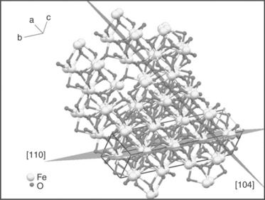
Figure 5.9 shows a family of XRD patterns obtained for a series of α-Fe2O3 photoelectrodes prepared by aerosol-assisted chemical vapour deposition at different deposition temperatures. All peaks not assigned to the SnO2 substrate such as [110], [104], [300], [012] and [024] were identified as hae- matite (JCPDS 33–0664). The [110], [104] and [300] are more pronounced than the other peaks. On the whole, the α-Fe2O3 XRD patterns are strong compared to the SnO2 patterns, indicating a high degree of crystallinity in the haematite films. The [104] peak is dominant for electrodes deposited at low temperatures suggesting that the α-Fe2O3 crystalline structure is pref- erentially oriented along the [104] direction. As the deposition temperature was gradually raised above 350°C while keeping all other parameter unchanged, the [104] peak diminished, and simultaneously the [110] peak became pronounced. This indicates that the preferential orientation of α-Fe2O3 in the [110] direction is favoured at high deposition temperatures. Figure 5.10 shows how the relative intensity ratio of [110]/([110]+[104]) of normalized XRD patterns varies with deposition temperature. Analysis of XRD patterns suggests that (i) electrodes deposited at low temperatures are oriented in such a way that the basal plane is preferentially aligned parallel to the FTO substrate, (ii) electrodes deposited at high temperatures are preferentially oriented, so that the c- axis is vertical to the substrate, (iii) there is a critical deposition temperature around 490°C where the relative ratio of [110]/([110]+[104]) reaches its maximum.
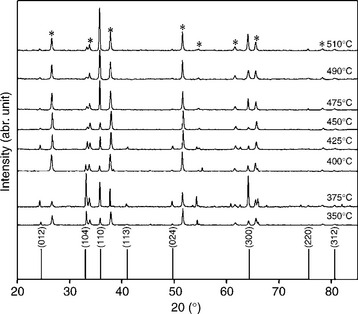
5.9 A family of XRD patterns obtained for a series of α-Fe2O3 photo- electrodes prepared by aerosol-assisted chemical vapour deposition at different deposition temperatures.
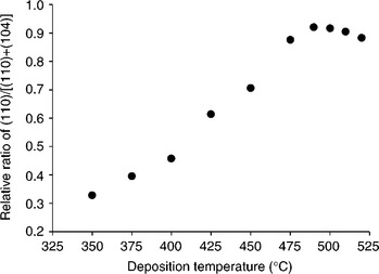
5.10 The relative intensity ratio of [110]/([110]+[104]) of normalized XRD patterns against the deposition temperature.
Figure 5.11 shows how VFB of α-Fe2O3 in 1 M NaOH varies as the relative intensity ratio of [110]/([110]+[104]) is changed by altering the α-Fe2O3 deposition temperature. At low deposition temperatures (~ 350°C), the rel- atively small [110]/([110]+[104]) intensity ratio suggests that the α-Fe2O3 surface is dominated by oxygen termination. As the deposition temperature is increased above 350°C, the [110]/([110]+[104]) intensity ratio gradually rises towards a maximum at 490°C, suggesting that the surface termination becomes dominated by Fe(III) groups. The observation of the most negative VFB when the [110]/([110]+[104]) intensity ratio is at its maximum is consistent with higher affinity of the Fe(III) surface for OH−. Figure 5.11 mirrors Fig. 5.10 suggesting that the negative shift of VFB is a direct result of the increased preferential orientation of α-Fe2O3 in the [110] direction. The magnitude of the negative shift is estimated to be about 0.32 V. Such a large negative shift in VFB. which corresponds to an upward movement of the conduction band relative to the hydrogen redox level, should reduce the external bias required to overcome the energetic mismatch at the α-Fe2O3/electrolyte interface. Indeed, this is the case, as revealed by PEC studies of these α-Fe2O3 electrodes.
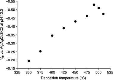
5.11 The change of VFB of α-Fe2O3 in 1 M NaOH as the relative intensity ratio of [110]/([110]+[104]) is changed by altering the α-Fe2O3 deposition temperature.
Plate III (see colour section between pages 238 and 239) compares the steady-state current–voltage characteristics of the series of α-Fe2O3 electrodes, and the inset shows their incident photon to electron conversion efficiency (IPCE%) spectra recorded at 0.23 V vs Ag/AgCl/3M KCl (− 1.23 V vs RHE). The J-V plot with the most negative photocurrent onset (Vonset) corresponds to the electrode that had the highest relative [110]/([110]+[104]) intensity ratio. Conversely, the J-V plot with the most positive Vonset is recorded for the electrode with lowest [110]/([110]+[104]) intensity ratio. When the α-Fe2O3 surface is preferentially oriented in this direction (i.e., the [110]/([110]+[104] ratio is lowest), the photocurrent transients for chopped illumination exhibited negative and positive spike characteristics for strong surface recombination. The photocurrent transients for electrodes preferen- tially oriented in the [110] direction did not show such spikes, suggesting the suppression of recombination. The absence of characteristic spikes in photocurrent transients and the negative shift of Vonset as the [110]/([110]+[104]) ratio is increased once again highlight the importance of the energetics of the semiconductor/electrolyte interface for photo-induced charge transfer kinetics. The negative shift of Vonset (approx. –0.32 V) closely follows the negative shift of VFB and is accompanied by an improved fill factor in the J-V plots suggesting low surface recombination. The other noticeable feature in Fig. 5.11 is the shift of dark-current onset potential of the α-Fe2O3 electrodes in the opposite direction to that of Vonset. The most negative dark-current onset corresponds to the α-Fe2O3 electrode that had the lowest [110]/([110]+[104]) ratio, whereas the most positive dark-current onset was observed for the electrode with the highest [110]/([110]+[104]) ratio. This may reflect the density of surface or defect states that can promote water oxidation under inversion conditions where electron transfer involves tunnelling across the space charge region in the a-Fe2O3. Water photo-oxidation and oxidation reactions have been studied on different surface terminations of rutile TiO2, and a significant variation of overpotential was predicted as the chemical environment of rutile surface is changed (Valdés et al., 2008). The incident photon-to-electron conversion efficiency (IPCE) at 0.23 V vs RHE also provides a useful insight into the competing processes at the a-Fe2O3 surface. As shown in the inset of Plate III, the IPCE increases as the photocurrent onset shifts in the negative direction accompanied by increased fill factor. The maximum IPCE was recorded for the electrode that had the highest [110]/([110]+[104]) ratio and hence the most negative VFB. The IPCE maximum recorded in this work (− 40%) is the highest value reported for an unmodified a-Fe2O3Fe2O3 electrode and indicates the potential of this approach. In principle, the same strategy can be used to manipulate energetics of other semiconductor/electrolyte interfaces to optimize the HER and OER under illumination in order to split water without an external bias.
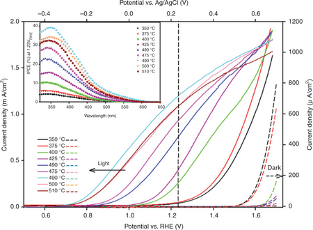
Plate III Comparison of the steady-state current voltage characteristics of α-Fe2O3 electrodes as the relative intensity ratio of [110]/([110]+[104]) is changed. The inset shows the corresponding incident photon to current conversion efficiency spectra recorded at 0.23 V vs Ag/AgCl/3M KCl (~ 1.23 V vs RHE).
5.5 Semiconductor photocathodes: material challenges
A photocathode/electrolyte interface can be incorporated into a photoelectrol- ysis cell either as the primary light-harvesting junction (in combination with an appropriate electrochemical anode) or as an optically complimentary photoac- tive half-cell in a dual photoelectrode tandem photoelectrolysis cell (Hamnett, 1982; Kocha et al, 1994). In the case of the former, the electrode should ideally harvest photon energy over most of the solar spectrum in order to yield the highest attainable energy conversion efficiency. However, in the latter case the photocathode may be only active in a particular bandwidth of the solar spectrum in order to generate a cathodic photocurrent that is sufficient to match the current generated in the photoanodic half-cell (Fig. 5.12). The energetics of a photocathode/electrolyte interface required for water splitting is shown in Fig. 5.5. As illustrated in both Figs 5.5 and 5.12, the Ecb of the cathodic semiconduc- tor material should be higher than the HER level to drive the reaction without external bias. Since the generation of one molecule of hydrogen involves only two photogenerated electrons, the mechanism of HER may be relatively less complicated than that of the OER. Typically, the HER mechanism is pH depen- dent such that it takes place via the reduction of protons at low pH whereas the reduction of water is the preferred route at high pH.
In terms of light-harvesting properties, p-Si is a suitable photocathode material due to its relatively small band gap of 1.12 eV. It has been used in a dual photoelectrode tandem photoelectrolysis cell (in conjunction with a suitable photoanode) to drive the HER. However, the main drawback of p-Si is the relatively low photovoltage (Dominey et al., 1982; Nakato et al, 1987; Hamann and Lewis, 2006). The Lewis and Atwater group has recently reported that PEC properties can be enhanced by using p-Si and n+ p-Si nanowire- based cathodes and by incorporating surface catalysts (Boettcher et al, 2010). p-GaInP2 has been extensively studied by Turner and co-workers (Khaselev and Turner, 1998). Their widely cited work reported a highly efficient mono- lithic water-splitting device incorporating a GaAs PV cell at the back of a p-GaInP2 electrode. The downside of p-GaInP2 is the mismatch between Evb and OER energy levels such that it is unable to split water without exter- nal assistance. This can be circumvented either by combining with a suitable anode and then applying a bias (the strategy adopted by Turner and co-workers) or by combining with a suitable photoanode that provides appropriate photovoltage. p-Cu2O has also been studied extensively as a possible photo- cathode for photoelectrolysis. Energetically, the p-Cu2O/electrolyte interface is similar to that of the p-GaInP2/electrolyte interface such that water oxida- tion is not possible on its own (Trasatti, 1992; de Jongh et al., 2000; Siripala et al., 2003). It is also notorious for rapid photocorrosion. Recent work on nanostructuring n-Cu2O has shown an enhanced photocurrent, a process that could be adapted for p-Cu2O to increase the PEC properties (McShane and Choi, 2009). Tennakone and co-workers have shown that Cu2O becomes rel- atively stable when it is incorporated onto TiO2 due to rapid charge transfer at the heterojunction (Senevirathna et al, 2005). In very recent work, Gratzel and co-workers have shown that p-Cu2O can be protected against photoca- thodic decomposition in water by coating the surface with thin conformal layers of Al-doped zinc oxide and titanium oxide by atomic layer deposition (Paracchino et al, 2011).p-GaP is another widely studied material, and HER under illumination has been demonstrated at its interface many years ago (emming and Schwandt, 1968; Aspnes and Studna, 1983). Like many other photocathodic materials, p-GaP has a very short minority carrier diffusion length which restricts the charge collection at the interface. Preparation of electrodes in textured form may be one way of circumventing that issue. p-InP is known for its near-IR region light absorption threshold (− 920 nm). The work con- ducted by Heller et al. in the early 1980s has shown promising solar conversion efficiencies in the order of 12–13% for water splitting using p-InP-based cells (Aharon-Shalom and Heller, 1982; Aspnes and Studna, 1983). Bockris et al. suggested that attaining solar conversion efficiency up to 18% for splitting water to hydrogen with p-InP (Pt-electrocatalyst)/n-Si (electrocatalyst) and up to 17% with p-Si (Pt)/n-InP(c) configuration is possible, if appropri- ate electrocatalysts are incorporated on the surface of n-Si and n-InP (Khan et al., 1988). Catalyst-coated p-InP has also been used along with n-MoSe2 and n-WSe2 electrodes to drive HER by decomposing HBr (Heller, 1983; Fornarini et al., 1984). However, the scarcity of indium has recently led to concerns of developing any technology that require indium-associated semi- conductors. The severe shortage of indium today could dramatically increase the cost and question the sustainability of photoelectrolysis, if the device configuration requires indium-based semiconductors (USGS, 2010; Kheraj et al., 2011).
p-SiC has also been considered as a cathodic semiconductor material for water-splitting device configurations (Sebastian et al., 2001; Akikusa and Khan, 2002; Dennis et al, 2009). Due to its wide optical band gap exceeding 3 eV, p-SiC is more suitable to be employed in a photosensitized device con- figuration (see Section 5.98). II-VI semiconductor photocathodes such as p-WSe2 and p-WS2 have been extensively studied to drive the HER in PEC cells (Fan et al., 1980; Baglio et al, 1983a, 1983b). The most recent exam- ples of use of II-VI materials for photoelectrolysis are studies of copper chalcopyrite photocathodes (p-Cu(In,Ga)Se2). Sebastian and co-workers reported PVD-deposited p-Cu(In,Ga)Se2 electrodes for photoelectrolysis (Valderrama et al, 2005). Miller et al. have been able to alter the band edges of p-Cu(In,Ga)Se 2 by changing the composition ratio of In:Ga (Marsen et al, 2008; Miller et al, 2010). Later, Tributsch and co-workers have reported the use of a protected photoelectrochemical tandem Cu(In,Ga)Se2 thin- film membrane for light-induced water splitting and HER (Neumann et al, 2009).
5.6 Advances in photochemical cell materials and design
5.6.1 New photoelectrode materials
Until the last decade, the studies of photoelectrolysis had been confined to a very few semiconductor material classes including metal oxides and III-V materials. For example, modifying wide band gap semiconductor oxides by doping has been traditionally a very popular route to extend the light absorption threshold to the visible part of the solar spectra (Jordan et al, 1972; D'Amico et al, 1984). The failure to develop efficient and sustainable photoelectrolysis cells from such semiconductors led to the extension of studies to new semiconductor material classes including binary, ternary and quaternary metal oxide compounds as well as non-oxide semiconductors. The energetics of many metal oxide semiconductors are poorly aligned with respect to the HER and OER potentials such that Ecb is generally below the H +/H2 energy level. Binary metal oxides such as metal titanates (i.e., SrTiO3, BaTiO3) deviate from that trend as the incorporation of second metal cat- ions (i.e., Sr.+, Ba2 +) results in a perovskite structure. This shifts the Ecb upwards and realigns the interfacial energetics in favour of photoelectrolysis (Walter et al., 2010). Modification of the perovskite materials such as titan- ates, niobates and tantalates has been conducted to incorporate O2- layers, and La2Ti2O7, K2La2Ti3O10, Ba5Nb4O15, Sr2Ta2O7 and Ba5Ta4O15 come under that category. It has been reported that such materials promote the OER through formation of catalytic centres (Kim, 2005). Another strategy was the incorporation of suitable elements with N2p and S3p orbitals into the crystal structure. The objective is to form a new energy level negative to Evb and extend the optical absorption threshold into the red region. BaTaO2N is an example for such semiconductors (Maeda, 2007). The commonly prac- ticed analogous approach is doping metal oxides with nitrogen, sulphur or carbon (Asahi, 2001). Metal oxides with d. 0 electronic configuration have also been looked at as another class of semiconductors suitable for photo- electrolysis due to their higher electronegativity (Sato, 2001, 2003, 2004). Metal ferrites are another class of semiconductor photoelectrode materials and studies have been conducted to investigate their optical and ener- getic properties with the focus of employing them in photoelectrolysis cells. Recent studies have identified ZnFe2O4 and CaFe2O4 as potential photo- anode and photocathode materials (Ida et al., 2010; Tahir and Wijayantha, 2010). Tungstates are another class of semiconductors recently investigated for photoelectrolysis (Chang et al., 2011). Woodhouse and Parkinson have developed a high-throughput combinatorial search strategy for the identification of multicomponent metal oxide materials with suitable bandgaps and band positions for water photoelectrolysis operating as either a photoanode or a photocathode (Woodhouse et al., 2005). Therefore, both synthesis of specifically designed new materials and combinatorial material discovery have opened up a completely new dimension to ongoing work on finding desirable semiconductors for photoelectrolysis in recent years (Woodhouse et al, 2005; Osterloh, 2008; Osterloh and Parkinson, 2011).
5.6.2 Tandem cells for photoelectrolysis
Cascade electrodes and tandem cells have been actively pursued to over- come light-harvesting limitations in photoelectrodes and energetic disparity between the band edges of known semiconductor materials and the HER and OER redox energy levels, respectively, in photoelectrolysis (Gratzel, 1989, 2001; Nozik, 1996; Khaselev and Turner, 1998; Wijayantha and Auty, 2005). Generally, photoelectrolysis tandem cells employ more than one photosystem that complement one another optically and energetically. For example, dual-photoelectrode tandem photoelectrolysis cell configuration (photoanode/electrolyte/photocathode) has been widely investigated since the 1980s to drive OER and HER on separate photoelectrodes (Hamnett, 1982). The energetics of a desirable dual photoelectrode tandem photo- electrolysis cell constructed by combining photoanodic and photocathodic junctions are given in Fig. 5.12. In this case, the photoanodic and photoca- thodic materials are chosen on the basis that their optical band gaps complement each other (to maximize the light-harvesting properties) and that the photocurrent density under operational condition in each electrode match the other.
An alternative tandem photoelectrolysis cell configuration is the combination of a photoanode/electrolyte interface with an optically comple- mentary solar cell. An analogous tandem cell can also be constructed by combining a photocathode/electrolyte interface with an optically comple- mentary solar cell (Nozik, 1996). The selection of appropriate semiconduc- tor photoelectrode and photovoltaic cell is primarily done on the basis of the optical absorption threshold of the photoelectrode in the photoelectrol- ysis cell and PV cell such that they complement each other (i.e., estimated attainable photocurrent density in each photosystem under operational condition matches as well as the bias voltage provided by PV cell is suffi- cient for alignment of the energetics of the semiconductor/electrolyte interface with HER and OER redox energy levels to drive photoelectrolysis). The energetics of such a tandem cell based on a photoanode are illustrated in Fig. 5.13 considering the energetics of n-WO3/electrolyte interface and a PV cell (Grätzel, 1989, 2001; Wijayantha and Auty, 2005). The illumination profile of this tandem cell in optically series and optically parallel configu- rations is shown in Figs 5.14 and 5.15, respectively. In the optically series configuration (Fig. 5.14), the bias voltage is provided by the solar cell which is illuminated by the spectral region unused by the photoelectrolysis cell (i.e., filtered light), hence no external bias is required. In contrast, each photosystem is illuminated by the entire solar spectra in the optically parallel configuration. The downside is the requirement of a large illuminated area to drive the same current density in the tandem cell. This needs to be taken into account in device efficiency calculation of the optically parallel configuration. Khaselev and Turner incorporated a GaAs PV cell at the back of a cathodic GaInP2/electrolyte junction in order to provide the necessary bias voltage to boost the free energy of photogenerated electrons to drive the HER at the interface (Khaselev and Turner, 1998). Similar approaches were also taken by others (Licht et al, 2000; Mauk et al, 2001).
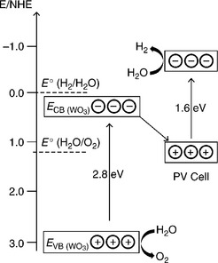
5.13 The energetics of a tandem photoelectrolysis cell based on n-WO3/electrolyte interface and a PV cell.
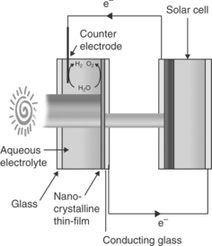
5.14 The illumination profile of a tandem photoelectrolysis cell in optically series configuration. Here, the photoelectrolysis cell absorbs the blue end photons of the sunlight whereas the remaining photons (red end photons) transmit through the electrolysis cell to the solar cell.
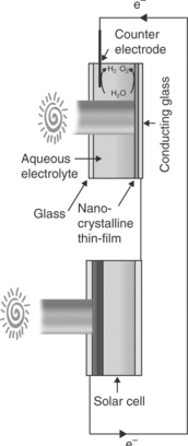
5.15 The illumination profile of a tandem photoelectrolysis cell in optically parallel configuration.
In principle, the reactions occurring in natural photosynthesis are analogues to the processes in tandem photoelectrolysis cells. However, the work conducted to date to construct photoelectrolysis prototype devices shows that the situation is not as simple as have been portrayed. The key components in photosynthesis are membranes, enzymes, etc., whereas the elements in tandem photoelectrolysis cell are semiconductors, liquid electrolytes and catalysts, etc. The energy conversion efficiency of photosynthesis is relatively low (~< 1% under natural light conditions) whereas it has to be significantly high in tandem cells. The photosynthetic reaction occurs at membranes of mono- or bi-layer (thickness of a few nanometres), allowing separation of oxidative and reductive products to prevent reverse reaction (Gerischer, 1977; Scheuring and Sturgis, 2006). The direct consequence of this is the weak light absorption, an issue that nature has been addressed by employing lamellar membrane stacks. A similar approach has been adopted in the DSC PEC cell to increase the light-harvesting efficiency (O'Regan and Grätzel, 1991). Further, one might say that nature understood the fact that all organic molecules undergo photodecomposition reactions sooner or later following the light absorption, and hence facilitated continuous regeneration of the photosynthetic system. Mimicking such a regeneration mechanism in a photoelectrolysis tandem cell to replenish photodecomposed materials is a very challenging and complex process. Another key conceptual differ- ence between natural photosynthesis and tandem photoelectrolysis cell is the absence of charge transport over a long distance in the photosynthesis. Unlike in photosynthesis, tandem photoelectrolysis cells operate on the basis that photogenerated electron–hole pairs are separated by transport through the semiconductor(s) in opposite directions before undergoing HER and OER reaction at the interfaces.
5.7 Interfacial reaction kinetics
The Gibbs free energy change for the generation of one mole of H2 by splitting one mole of water under standard conditions is 237.2 kJ. This accounts for 2.46 eV (i.e., 1.23 eV per electron transfer). If the photo- electrolysis cell is based on a photocathode, the photo-induced process should generate and separate two electron–hole pairs, and then facilitate electron transfer at the semiconductor/electrolyte interface to drive HER. Similarly, the light absorption should generate and separate four electron- hole pairs and then facilitate the hole transfer at the semiconductor/elec- trolyte interface to drive the OER in a photoanode-based electrolysis cell. Hence, the semiconductor electrode materials employed in photoelec- trolysis cells should be capable of facilitating rapid charge transfer at the interface. Unless the charge transfer kinetics under photostationary condi- tion is rapid enough to circumvent interfacial recombination losses, a significant part of available free energy at the illuminated interface will not be recovered. Lewis explained this dynamic situation with the aid of the LeChatelier's principle such that the photovoltage at an interface is zero at equilibrium (i.e., dark). The charge carriers created under illumination will tend to recombine at the interface so as to oppose the perturbation of the system due to the light absorption. Illumination of the interface with high light intensities will thus create a stronger tendency for the system to return to its equilibrium condition (Lewis, 2005). The externally measured photocurrent in a PEC cell is the net result of competition between the surface recombination and interfacial charge transfer across the semicon- ductor/electrolyte interface.
The charge transfer kinetics at illuminated semiconductor/electrolyte interface has been reported in a number of previous studies (Hamnett, 1987; Peter, 1990, 1999; Memming, 1994; Salvador, 2001; Lewis, 2005). We have recently considered the photo-induced OER kinetics of the α-Fe2O3/NaOH interface (Cummings et al, 2012a, 2012b; Peter et al, 2011; Wijayantha et al, 2011). Losses due to surface recombination of photogenerated electronhole pairs play a key role in determining the efficiency of α-Fe2O3 photoanodes (Albery and Bartlett, 1981; Lemasson et al, 1982; Landsberg, 1991). The low mobility and short lifetime of holes combined with the high doping levels in α-Fe2O3 electrodes lead to poor collection of holes from the bulk of the material to the surface. The problem of the short hole diffusion length L in α-Fe2O3 has been addressed by fabricating nanostructured films in which the characteristic dimensions are comparable with L, so that holes have an increased chance of reaching the surface. However, even in the case where holes are collected efficiently in the space charge region and transferred to the semiconductor surface, the interfacial hole transfer leading to the oxida- tion of water has to compete with surface recombination. Little is known about the kinetics of these competing processes in the case of α-Fe2O3. The mechanism of PEC oxygen evolution on α-Fe2O3 must involve the transfer of four electrons per molecule of O2 formed, but almost nothing is known about the individual elementary steps in the reaction. It is reasonable to suppose that the reaction steps in the OER involve higher valent states of iron formed at the surface by hole capture. In fact, the recent work conducted by Sarma et al (2012) suggests that water oxidation is mediated by the Fe(IV) species. Figure 5.16a illustrates the complications arising from the fact that the oxidation of water is a four-electron process, so that holes need to be 'stored' in intermediate states. The Fe(IV) and Fe(V) intermediates in Fig. 5.16a can also act as electron acceptors, so that surface recombination reac- tions of the kind shown in Fig. 5.16b are likely to take place.
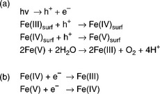
5.16 (a) This scheme illustrates the complications arising from the fact that the oxidation of water is a 4-electron process, so that holes need to be 'stored' in intermediate states. (b) This scheme shows the Fe(IV) and Fe(V) intermediates that also act as electron acceptors in the process.
The Fe(IV) and Fe(V) states can also be thought of as 'surface-trapped holes', which may have sufficient surface mobility to allow second-order reactions of the type illustrated by the last step shown in Fig. 5.16a. The rate expressions derived from these kinetic schemes are generally rather cumbersome, since they include rate constants and surface concentrations for all of the intermediates and reaction steps. It is therefore more con- venient to adopt a simpler phenomenological approach for the analysis of experimental data. The rate constants obtained from such an analysis can then be related to the expressions derived for different multistep reaction mechanisms (Peter et al, 1997). This approach can be used to analyse data obtained by photoelectrochemical impedance spectroscopy (PEIS). The results provide useful information about the rate constants for the competing processes that determine the performance of α-Fe2O3 photoanodes.
The simplest phenomenological scheme to describe the competition between charge transfer and recombination at an illuminated n-type semiconductor is illustrated in Fig. 5.17. It has been assumed that electron transfer and recombi- nation involve surface states (in principle, these can be the intermediates in the reaction schemes described previously). Competition between the overall rates of hole transfer and recombination determines the fraction of the hole current jh that is measured in the external circuit. This fraction corresponds to the internal quantum efficiency of the process. The scheme shown in Fig. 5.17 is a simplified model used by Peter et al. previously to discuss the phenomenological approach and its application to PEIS since it excludes direct hole transfer from the valence band to solution redox species (Ponomarev and Peter, 1995; Schlichthörl et al., 1995; Peter et al., 1997). This simplification is clearly appropriate in the absence of a one-electron redox couple in the electrolyte. The phenomenological first- order rate constants kt and kr (s−1) appearing in Fig. 5.17 and in the equations for the PEIS response are used to express the rates of hole transfer and recombina- tion (cm−2 s−1) in terms of the surface concentration of 'trapped holes' (cm−2).
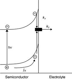
If Fig. 5.16a and 5.16b is considered as an example of a possible mechanism, the surface trapped holes correspond to Fe(IV) and Fe(V) species. 'Hole transfer' in this formalism therefore corresponds to the overall four- electron oxidation process leading to the formation of oxygen. Similarly, the recombination process corresponds to electron capture by Fe(IV) and Fe(V) species, which can be thought of as photogenerated surface recombi- nation centres. The rate of the recombination process depends on the electron capture cross-sections and surface concentrations of Fe(IV) and Fe(V) species ('trapped holes') as well as on the concentration of free electrons available at the surface. It follows that kr should depend on band bending qΔϕSC, since the electron concentration at the surface is given by
where nbulk is determined by the doping density. For highly doped semiconductors like Fe2O3, recombination may also involve electron tunnelling through the space charge region. For the case where the Helmholtz capacitance is larger than the space charge capacitance, it has been shown that the impedance of the illuminated electrode is given by Equation [5.14] (Ponomarev and Peter, 1995).
where Rser is the series resistance, Csc is the space charge capacitance, jh is the current density corresponding to the flux of holes reaching the interface, and kt and kr are the first-order rate constants for interfacial transfer and recombination, respectively (Fig. 5.17). The impedance described by Equation [5.15] corresponds to two semicircles in the complex plane. The low-frequency semi- circle (LF) tends towards a zero-frequency intercept on the real axis given by
The radial frequency ωmax(LF) corresponding to the maximum imagi- nary component of the low-frequency semicircle is equal to kt. The high- frequency limit of the low-frequency semicircle is
Relations [5.15] and [5.16] follow:
The radial frequency ωmax (HF) corresponding to the maximum imaginary component of the high-frequency semicircle is given by 1/[Csc(Z2 – Rser)]. For polycrystalline highly doped semiconductors like α-Fe2O3, the jh is expected to be smaller than qI0, since electron–hole pairs generated outside the space charge region are mostly lost by recombination. In addition, electron–hole recombination in the space charge region may also reduce jh. It can be seen from the earlier equations that kt, kr, Csc and jh can be determined experimen- tally from the PEIS response shown schematically in Fig. 5.18. Leng et al. have reported a comprehensive work which presents more general expressions for the PEIS response considering the case where the space charge capacitance is not smaller than the Helmholtz capacitance. They also included the effects of surface state capacitance as well as the possibility that kt is influenced by the potential drop in the Helmholtz layer (Leng et al, 2005).
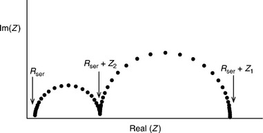
5.18 Typical PEIS response predicted by Equation [5.15].
Normalized photocurrent voltage plots for α-Fe2O3 electrodes recorded at three different light intensities are shown in Fig. 5.19. The peak IPCE at 350 nm is 13% at 0.23 V vs Ag|AgCl, which is lower than the values for thinner nanostructured electrodes. The PEIS measurements were carried out at longer wavelengths (455 nm), where the IPCE is around 2%. Such low IPCE values confirm the estimation that the majority of electron–hole pairs are generated outside the space charge region and recombine in α-Fe2O3.
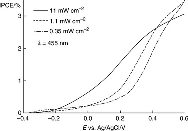
5.19 Normalized photocurrent (IPCE) voltage curves recorded at three light intensities (455 nm LED illumination).
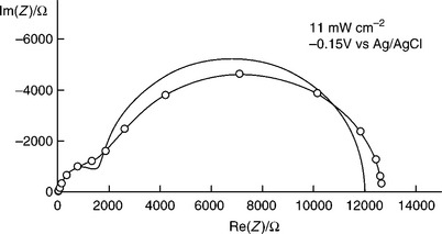
It can be seen from Fig. 5.19 that the normalized photocurrent in the range − 0.4 to 0.4 V increases with illumination intensity so that the photocurrent onset shifts towards more negative potentials. There are several possible reasons for this behaviour, including space charge and surface recombination as well as the kinetics of the multi-electron transfer pro- cess (Abrantes and Peter, 1983; Peter et al., 1984, 1997; Li et al, 1984; Li and Peter, 1986; Vanmaekelbergh and Cardon, 1988; Fermin et al, 1999). The presence of surface recombination in this potential region is evident from the spikes and overshoots in the photocurrent response to chopped illumination. Therefore, PEIS measurements were carried out in the onset region to obtain information about the competition between hole transfer and recombination whilst maintaining the dc illumination intensities at the same levels as shown in Fig. 5.19. The measured PEIS responses generally showed the two semicircles predicted by Equation [5.15]. An example with the fitting is shown in Fig. 5.20. The flattening of the PEIS response that is evident in the Nyquist plot may arise from a dispersion of kinetic parameters or from dispersion in the dielectric constant of α-Fe2O3 (Papaioannou et al., 2005).
PEIS spectra were fitted and analysed to obtain kt, kr, Csc and jh as a function of potential at three light intensities. Figure 5.21 illustrates a set of data obtained at 1.1 mW cm-2.
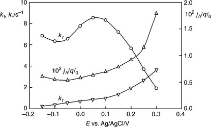
5.21 The kt and kr and jh are derived from the analysis of PEIS spectra recorded at 1.1 mW cm-2 dc illumination intensity. The right-hand scale corresponds to the IPCE that would be measured in the absence of surface recombination.
The variation of the recombination rate constant kr with potential indi- cates that the semiconductor/electrolyte junction is not behaving ideally. kr depends linearly on the surface electron concentration nsurf, which for an ideal semiconductor/electrolyte junction decreases by a factor of 10 per 59 meV of increased band bending. The plot of kr vs potential passes through a maximum before falling as expected for increasing band bending. This indicates that the band bending varies little over the initial potential range, a behaviour that is typical for Fermi level pinning associated with a high density of surface states as reported by Dare-Edwards et al. (1983). As shown below, it appears as if the surface states are photoinduced in the present case, and the most likely explanation is that they are associated with higher valent iron species formed by hole capture. The increase with potential of kt, the rate constant for electron transfer, differs from the behaviour observed in more ideal systems, where kt is found to be independent of potential. Since the increase in kt with potential is observed in the potential range where Fermi level pinning occurs and the majority of the change in potential appears as a voltage across the Helmholtz layer, we assume that it indicates that the phenomenological rate constant for oxygen evolution is influenced by the potential drop across the Helmholtz layer.
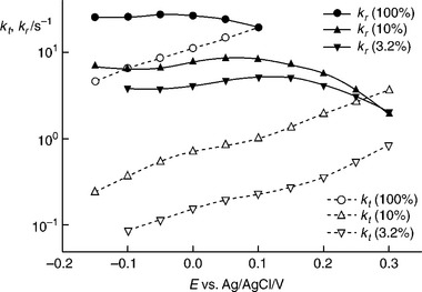
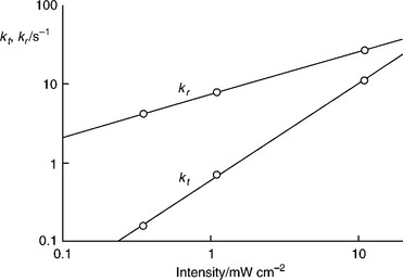
Figure 5.22 contrasts the kt and kr values obtained from the analysis of PEIS spectra measured for three different illumination intensities. A loga- rithmic y-scale has been chosen to show that the variation of kt with potential corresponds to a Tafel slope of circa 350 mVmV/decade for all three intensities. Tafel slopes for oxygen evolution of thin passivating α-Fe2O3 films on iron in the dark have been reported by Lyons and Brandon to lie in the range 40–50 mV (Lyons and Brandon, 2009). The weaker potential dependence in the present case may be related to the lower fraction of the overall potential drop that appears across the Helmholtz layer. Both kt and kr depend on light intensity, with kt varying more strongly with intensity than kr. The variation of kt and kr with intensity is illustrated in the double logarithmic plots shown in Fig. 5.23. The values of the rate constants were taken from Fig.5.22 at a potential of 0 V vs Ag|AgCl. It can be seen from Fig.5.23 that kr varies with I00–54, which is close to a square root dependence. By contrast, kt varies with I01.2, which is close to a linear dependence. In principle, these intensity dependenties could be related to possible mechanisms of the oxygen evolution. The different intensity dependencies explain why the photocurrent onset moves towards more negative potentials with increasing light intensity.
The fraction of the hole flux that is consumed in the OER as opposed to recombination is determined by the ratio kt(kt + kr), which has been plotted as a function of potential in Fig. 5.24. The validity of the analysis is demonstrated by the fact that the plots in Fig. 5.24 mirror the photocurrent voltage plots in Fig. 5.19. It is therefore clear that the delayed photocurrent onset at relatively low light intensities can be attributed to surface recombina- tion and Fermi level pinning. In order to overcome this problem, it will be necessary to remove the kinetic bottleneck that leads to the build up of intermediates that 'metallize' the surface and promote recombination by capturing electrons.
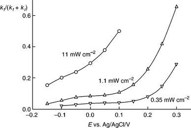
PEIS can provide information about the phenomenological rate constants describing the competition between charge transfer and recombination during OER at illuminated electrode/electrolyte interface. The complex potential dependence of the rate constants for these two processes highlights the non-ideal nature of the α-Fe2O3/electrolyte interface arising from photogenerated surface species. Efficient water splitting in a tandem photoelectrochemical cell using α-Fe2O3 as a photoanode requires that the photocurrent onset should be as close to the flatband potential as possible (i.e., ideally near − 0. 6 V vs Ag|AgCl in 1.0 M NaOH ≈ 0.8 V negative of the reversible oxygen electrode potential). A positive displacement of the photocurrent onset represents a loss of available free energy and hence low efficiency. Clearly this means that accumulation of positive surface charge associated with Fermi level pinning and changes in surface composition must be avoided as far as possible. Since the accumulation of electronic and ionic surface charge appears to be associated with sluggish hole transfer kinetics, it should be possible to overcome the effects by using a suitable surface catalyst for the OER.
5.8 Future trends
5.8.1 Hydrogen evolution reaction and oxygen evolution reaction catalysts
The previous section suggested that even if semiconductor materials with desirable energetics are used in PEC reactions, the slow interfacial kinetics may still limit the overall efficiency. The overpotentials required to overcome the kinetic limitations in OER and HER are significantly responsible for the low efficiency in photoelectrolysis. The previous section also highlighted the non-ideal nature of illuminated semiconductor/electrolyte interface in general and showed the need of incorporating catalysts on semiconductor surface to reduce the overpotential (Wijayantha et al, 2011). In order to act as a successful catalyst, it requires satisfying at least two basic requirements (it must be highly active toward the reaction(s) of interest and robust enough to maintain catalytic activity over sufficiently long period of time). As OER is a four-electron transfer process, it is thought to be the main contributor to the loss associated with kinetic overpotentials in photoelectrolysis. Heller showed that the recombination velocity of photogenerated electrons at the semiconductor-catalyst interface must be low (Heller, 1983). For electrocat- alytic water oxidation, the typical overpotential on Co3O4 incorporated Co electrodes in basic electrolytes are reported to be between 350 and 400 mV at 10 mAcm-2 current density. On the other hand, the desired target overpo- tential for OER at illuminated anodic semiconductor/electrolyte interface is in the order of 100–200 mV for the same magnitude of photocurrent density (Chou et al, 2011). This highlights the challenge in developing efficient photoanodic half-cells to drive OER RuO2, MnOx, IrO2, Co3O4, NiCO2O4, Pt, Pd, Ru–Co, Ru–Ir, Ru–Cu are some well-known metal oxide, metallic and bi-metallic electrocatalysts that already used for this purpose at moderate overpotential and relatively high current densities (Trasatti and Lodi, 1981; Forgie et al, 2010). Lewerenz et al. recently reported that solar-to-hydrogen conversion efficiency reach 12.1% for homoepitaxial InP thin-films covered with Rh nanoislands (Lewerenz et al, 2010). Despite the extensive work on binary and ternary electrocatalysts, Pt has been the popular choice of OER catalyst on the surface of many semiconductor photoanodes (Harris and Kamat, 2010; Rosseler et al., 2010). Nocera and co-workers have recently reported a new class of electrocatalysts based on cobalt phosphate and borate to drive OER, and the current density as high as 100 mA/cm2 has been achieved at 350 mV overpotential by employing them (Esswein et al, 2011). The potential of such catalysts has been demonstrated by incorpo- rating them on n-Si surface to drive OER at a significantly low overpotential (Young et al, 2011). As for the HER catalysts, there are two main types used to date: namely metal composites/alloys and non-metallic compounds. Among catalysts investigated, nickel and Ni-containing binary and ternary metallic catalysts have shown the performance to be as good as that of Pt (Conway et al, 1983; Wendt and Plzak, 1983; Endoh et al, 1987; Raj and Vasu, 1990; Raj, 1993; Hu et al, 1995; Walter et al, 2010). Such catalysts have been incorporated to reduce the HER overpotential at illuminated p-Si junction to achieve cathodic photocurrent densities as high as 12 mAcm−2 in pH 4.5 by Lewis and Gray group in Caltech (McKone et al, 2011).
5.8.2 Stability of photoelectrodes
One of the serious challenges in development of practical PEC cells based on the semiconductor/electrolyte interface (i.e., regenerate PEC cells and photoelectrolysis cells) is, retaining the electrode stability over a prolonged operation. Anodic oxidation and cathodic reduction are well- known routes of electrode material deterioration and may occur under illumination or external bias in the dark (Gerischer, 1977). The driving force for these electrochemical processes is the free energies of holes and electrons, respectively. As illustrated in Fig. 5.2, these free energies are represented by pEF and nEp under illumination. If pEp is positive to the anodic decomposition (oxidation) potential of a particular material, it oxidizes under illumination. Similarly, if nEF is negative to the cathodic decomposition (reduction) potential it under- goes reduction. Semiconductor materials degradation/dissolution influenced by illumination are commonly referred to as photocorrosion. CdS, ZnO, Cu2O, Si and GaAs are well-known semiconductor photoelectrode materials that undergo photocorrosion (Morrison, 1980; Meissner et al, 1987; Zhang et al, 2009). Studies have been conducted to circumvent both photo-oxidation and photoreduction by surface modifications, protective coatings and cata- lytic incorporation (Hodes et al, 1983; Pijpersa et al, 2011).
5.8.3 New frontiers for photoelectrolysis cells
It has been 40 years since photoelectrolysis was first demonstrated (Fujishima and Honda, 1972). Since then, numerous efforts have been made not only by chemists, physicists, engineers and materials scientists in technology development, but also by economists, investors, policy makers, entrepreneurs, environmental lobbyists and enthusiasts in promoting the concept. Despite that, we are still waiting to see a photoelectrolysis device that is efficient, affordable, stable for a prolonged operation, scalable and hence, commercially attractive for long-term and large industrial scale invest- ments. Nevertheless, tremendous progress has been made in many areas directly or indirectly related to photoelectrolysis. In terms of the science and technology of semiconductor photoelectrolysis, the work conducted up to now suggests that the key challenges are associated with finding desira- ble semiconductor materials, understanding the fundamental processes in photoelectrolysis that matters in device operation and addressing the com- patibility issues of key components in device construction. Besides, a significant increase of the demand for hydrogen is essential to trigger large-scale investments for semiconductor photoelectrolysis. This final section provides an overview of the future research directions and emerging new frontiers in semiconductor photoelectrolysis.
As already highlighted, finding desirable semiconductor photoelectrode materials that meet the stringent criteria for photoelectrolysis has always been a key challenge. Generally, a few routes are available to pursue and meet this challenge (i.e., continue current efforts to design and discover new materials, attempt to alter the interfacial energetics and charge transfer properties of known semiconductors). A brief summary was given in Section 5.4 with a few notable examples of recent advances in finding new materials with appreciable PEC properties. Such efforts need to be continued with the focus not only on light-harvesting properties but also on interfacial energetics and charge transfer properties of targeted new materials. Many complex oxides are known for their low charge mobility and short minority carrier lifetime. Therefore, as already discussed, construction of electrodes with such materials in textured form (i.e., nanostructuring) may circumvent the charge recombination in bulk as well as within the space charge region (Tahir and Wijayantha, 2010). However, the use of very fine nanoscale features containing photoelectrodes can also be introduced some unwanted complications for the photoelectrolysis device operation. For example, driv- ing HER or OER with a decent photocurrent density (i.e., 10 mAcm−2) on a nanostructured electrode may build a steep local pH gradient within the high porous matrix due to mass transport limitations in the liquid phase which could eventually cause corrosion/dissolution of semiconductor elec- trode material as well as alter the energetics at the interface with respect to redox potentials in bulk electrolyte. Therefore, the average feature size (of porous electrodes) should be carefully controlled during electrode prepa- ration by considering such effects. Construction of textured semiconductor electrodes has been mainly achieved to date by following well-documented bottom-up protocols (Hodes et al, 1992; Rothenberger et al, 1992; Barbé et al. 1997; Goh et al, 2005; van de Krol et al, 2008; Sivula et al, 2010). Surprisingly, very little attention has been paid to date for texturing semiconductor electrodes for PEC applications by top-down approaches (Keis et al, 1999; Pacholski et al, 2002; Peng et al, 2007). Electrodes prepared by top- down methods have shown novel properties and found applications in many devices (Sun et al., 2006; Kislyuk and Dimitriev, 2008). In fact, top-down methods offer unique advantages over bottom-up methods particularly in semiconductor photoelectrode preparation with desired PEC properties (i.e., ability to etch off specific surface facets selectively that promote inter- facial recombination, flexibility of starting with flat films of crystalline materials which may have better charge mobility) (Hollan et al, 1979). Therefore, more attention should be devoted to the preparation of textured electrodes for photoelectrolysis by top-down techniques.
The work conducted by us and others show that engineering energetics of known semiconductor materials in favour of photoelectrolysis by manipu- lating preferential orientation is a promising method (Section 5.4.3). Such efforts may be continued and extended to unravel the true potential of known semiconductors which have left out due to the polycrystalline nature of photoelectrodes tested to date. Along with such efforts, other parallel strategies such as construction of smaller band gap heterojunction photo- electrodes needs to be continued to align interfacial energetics in favour of unassisted photoelectrolysis, provided that key semiconductor properties such as energetics, light absorption and stability complement each other. Surface derivatization by covalent chemical modification to control the band energies at the semiconductor/electrolyte interface, and then eliminate the pH dependence of the band edges, is an area that requires further work. Also, the protection of the surface of electrode materials known for corro- sion by incorporating ultra-thin-films of stable oxides is another emerging area of interest following the recent work conducted on Cu2O and α-Fe2O3 to increase PEC properties and stability (Le Formal et al, 2011; Paracchino et al, 2011). The work conducted to study materials such as α-Fe2O3 shows that slow interfacial kinetics and accumulation of surface charge is associated with Fermi level pinning and changes in surface composition that must be avoided to improve the PEC properties at the semiconductor/electro- lyte interface (Section 5.7). As discussed in Section 5.8, this can be achieved by incorporating HER and OER catalysts on the semiconductor surface. Although Pt has been the widely used OER catalyst on many semiconduc- tor photoanodes, a significant overpotential is still required even after Pt incorporation (Bockris and Huq, 1956; Rosseler et al, 2010). Further work is required to find new electrocatalysts that are stable (resistive to corro- sion and poisoning and retain the catalyst properties without undergoing compositional or morphological changes) and that can be incorporated on the semiconductor surface. In order to achieve this, an understanding of reaction mechanisms is required (i.e., awareness of the rate determining step(s), intermediates and suitable catalysts to overcome the kinetics). This requires further work and the recent efforts made by us and others need to be continued (Cowan et al, 2011; Cummings et al, 2012a, 2012b; Pendlebury et al, 2011; Peter et al. 2011; Wijayantha et al, 2011).
As already discussed, metal oxides such as α-Fe2O3 and WO3 have been extensively studied as photoanodic electrode materials for water splitting. In order to use them in water splitting cells an external bias voltage is required. Tandem water splitting cell configuration offers a solution for this as such an optically parallel or series mounted PV cell provides the necessary bias voltage. Section 5.6 provided a brief overview of photo- electrolysis tandem cell configurations. It is an attractive way of splitting water using the visible light. In fact, photoelectrolysis by visible light has been a challenge for many decades (Wrighton, 1979; Bard and Fox, 1995). Some work has already been done in order to construct and test industrial-scale tandem cells for photoelectrolysis. For example, a UK-based company Hydrogensolar Ltd successfully constructed prototype photoelectroly- sis devices based on the tandem concept (see Fig. 5.25). Further work is required to understand the fundamental limitation of these devices in order to make them robust, stable and the individual device components are chemically compatible. Dye sensitization is an alternative way of using visible light for photoelectrolysis and the concept has been already proven (Youngblood et al, 2009; Sun et al, 2010). Although the performance reported to date for the photoelectrolysis cells based on dye-sensitization is still poor, the advances made in understanding photoinduced electron transfer reactions in molecular donor-acceptor dyads and in sensitizer- semiconductor dyads could be very useful to make further advances in that area. The low efficiency reported for such systems is mainly due to the degradation of the oxidized dye molecules as the kinetic pathways of water oxidation are very slow. The band energies of wide band gap semi- conductors such as SiC, SrTiO3 and KTaO3 are favourable for unassisted PEC water splitting, they could be useful materials for sensitization with appropriate dye molecules.
Organic molecules and semiconductors undergo photodecomposition reactions sooner or later following the light absorption. In order to over- come this, nature facilitates continuous regeneration of the photosynthetic system. Mimicking such regeneration mechanism in photoelectrolysis to replenish photodecomposed materials is a very challenging and complex problem to solve. Inspired by the photosynthesis performed by plants, Nocera and his team at the Massachusetts Institute of Technology have combined a catalyst with photovoltaic cells to achieve nearly 100% elec- trolysis (Esswein and Nocera, 2007; Surendranath et al, 2010; Esswein et al, 2011). This is a major breakthrough in the recent history towards mimicking photosynthesis efficiently to generate hydrogen. A detailed account of his work is beyond the scope of this chapter. However, the efforts by Nocera and co-workers could be a catalyst for further advancements for the generation of hydrogen from sunlight at an affordable cost in the near future.
5.9 Acknowledgements
The work reported in Section 5.7 was conducted in collaboration with Professor Laurie Peter, Department of Chemistry, University of Bath, UK. We are grateful to him for kindly taking time to read the first draft of this chapter and providing valuable suggestions and comments. The work reported in Section 5.4.3 was conducted in collaboration with Dr Asif Ali Tahir when he was a postdoctoral research fellow at Renewable Energy Research Group in the Department of Chemistry, Loughborough University, UK. We would like to acknowledge the untiring assistance given by Nirmal Peiris to prepare this chapter. Stored Solar Ltd is acknowl- edged for providing the photographs of prototype photoelectrolysis cells (Fig. 5.25).
5.10 References
Abrantes, L.M., Peter, L.M. Transient photocurrents at passive iron electrodes. J Electroanal Chem. 1983; 150:593–601.
Aharon-Shalom, E., Heller, A. Efficient p-lnP(Rh-H alloy) and p-lnP(Re-H alloy) hydrogen evolving photocathodes. J Electrochem Soc. 1982; 129:2865–2866.
Akikusa, J., Khan, S.U.M. Photoelectrolysis of water to hydrogen in p-SiC/Pt and p-SiC/n-TiO2 cells. Int J Hydrogen Energ. 2002; 27:863–870.
Albery, W.J. Development of photogalvanic cells for solar energy conversion. Acc Chem Res. 1982; 15:142–148.
Albery, W.J., Bartlett, P.N. The transport and kinetics of minority carriers in illuminated semiconductor electrodes. J Electrochem Soc. 1981; 128:1492–1501.
Archer, M.D., Nozik, A.J. Nanostructured and photoelectrochemical systems for solar photon conversion. London: Imperial College Press; 2008.
Aspnes, D.E., Heller, A. Photoelectrochemical hydrogen evolution and water-photolyzing semiconductor suspensions: Properties of platinum group metal catalyst-semiconductor contacts in air and in hydrogen. J Phys Chem. 1983; 87:4919–4929.
Aspnes, D.E., Studna, A.A. Dielectric functions and optical parameters of Si, Ge, GaP, GaAs, GaSb, InP, InAs, and InSb from 1.5 to 6.0 eV. Phys Rev B. 1983; 27:985–1009.
Bard, A.J., Fox, M.A. Artificial photosynthesis: Solar splitting of water to hydrogen and oxygen. Acc Chem Res. 1995; 28:141–145.
Baglio, J.A., Calabrese, G.S., Harrison, D.J., Kamieniecki, E., Ricco, A.J., Wrighton, M.S., Zoski, G.D. Electrochemical characterization of p-type semi- conducting tungsten disulfide photocathodes: Efficient photoreduction pro- cesses at semiconductor/liquid electrolyte interfaces. J Am Chem Soc. 1983; 105:2246–2256.
Baglio, J., Kamieniecki, E., Decola, N., Struck, C., Marzik, J., Dwight, K., Wold, A. Growth and characterization of n-WS2 and niobium-doped p-WS2 single crystals. J Solid State Chem. 1983; 49:166–179.
Barbé, C.J., Arendse, F., Comte, P., Jirousek, M., Lenzmann, F., Shklover, V., Grätzel, M. Nanocrystalline titanium oxide electrodes for photovoltaic applications. J Am Ceram Soc. 1997; 80:3157–3171.
Bockris, J.O.M., Huq, A.K.M.S. The mechanism of the electrolytic evolution of oxygen on platinum. Proc R Soc Lond A. 1956; 237:277–296.
Boettcher, S.W., Warren, E.L., Putnam, M.C., Santori, E.A., Turner-Evans, D., Kelzenberg, M.D., Walter, M.G., McKone, J.R., Brunschwig, B.S., Atwater, H.A., Lewis, N.S. Photoelectrochemical hydrogen evolution using Si microwire arrays. JAm Chem Soc. 2010; 133:1216–1219.
Bolton, J.R. Solar fuels. Science. 1978; 202:705–711.
Bolton, J.R. Solar photoproduction of hydrogen: A review. Solar Energy. 1996; 57:37–50.
Bolton, J.R., Strickler, S.J., Connolly, J.S. Limiting and realizable efficiencies of solar photolysis of water. Nature. 1985; 316:495–500.
Bookbinder, D.C., Bruce, J.A., Dominey, R.N., Lewis, N.S., Wrighton, M.S. Synthesis and characterization of a photosensitive interface for hydrogen gen- eration: Chemically modified p-type semiconducting silicon photocathodes. Proc Natl Acad Sci. 1980; 77:6280–6284.
Cesar, I., Kay, A., Martinez, J.A.G., Grätzel, M. Translucent thin film Fe2O3 photoanodes for efficient water splitting by sunlight: Nanostructure directing effect of Si-doping. JAm Chem Soc. 2006; 128:4582–4583.
Chang, Y., Braun, A., Deangelis, A., Kaneshiro, J., Gaillard, N. Effect of ther- mal treatment on the crystallographic, surface energetics, and photoelectro- chemical properties of reactively cosputtered copper tungstate for water splitting. J Phys Chem C. 2011; 115:25490–25495.
Cheng, J., Zhanga, H., Ma, H., Zhong, H., Zou, Y. Study of carbon-supported IrO2 and RuO2 for use in the hydrogen evolution reaction in a solid polymer electrolyte electrolyzer. Electrochim Acta. 2010; 55:1855–1861.
Chen, Z., Jaramillo, T.F., Deutsch, T.G., Kleiman-Shwarsctein, A., Forman, A.J., Gaillard, N., Garland, R., Takanabe, K., Heske, C., Sunkara, M., McFarland, E.W., Domen, K., Miller, E.L., Turner, J.A., Dinh, H.N. Accelerating materials development for photoelectrochemical hydrogen production: Standards for methods, definitions, and reporting protocols. J Mater Res. 2010; 25:3–16.
Chou, N.H., Ross, P.N., Bell, A.T., Tilley, T.D. Comparison of cobalt – based nanoparticles as electrocatalysts for water oxidation. Chem Sus Chem. 2011; 4:1566–1569.
Conway, B.E., Angerstein-kozlowska, H., Sattar, M.A., Tilak, B.V. Study of a decomposing hydride phase at nickel cathodes by measurement of open-circuit potential decay. J Electrochem Soc. 1983; 130:1825–1836.
Cowan, A.J., Barnett, C.J., Pendlebury, S.R., Barroso, M., Sivula, K., Grätzel, M., Durrant, J.R., Klug, D.R. Activation energies for the rate-limiting step in water photooxidation by nanostructured α-Fe2O3 and TiO2. J Am Chem Soc. 2011; 133:10134–10140.
Cummings, C.Y., Marken, F., Peter, L.M., Tahir, A.A., Wijayantha, K.G.U. Kinetics and mechanism of light-driven oxygen evolution at thin film α-Fe2O3 electrodes. Chem Comm. 2012; 48:2027–2029.
Cummings, C.Y., Marken, F., Peter, L.M., Wijayantha, K.G.U., Tahir, A.A. New insights into water splitting at mesoporous α-Fe2O3 films: A study by modulated transmittance and impedance spectroscopies. J Am Chem Soc. 2012; 134:1228–1234.
D'Amico, A., Grilli, A., Paoletti, A., Paroli, P., Tucciarone, A. Doped yttrium iron garnet for thermistor-bolometers. Mat Res Bull. 1984; 19:347–354.
Dare-Edwards, M.P., Goodenough, J.B., Hamnett, A., Trevellick, P.R. Electrochemistry and photoelectrochemistry of iron (III) oxide. J Chem Soc Faraday Trans. 1983; 1(79):2027–2041.
de Jongh, P.E., Vanmaekelbergh, D., Kelly, J.J. Photoelectrochemistry of electrodeposited Cu2O. J Electrochem Soc. 2000; 147:486–489.
van Dorp, Dennis H., Hijnen, Niek, Di Vece, Marcel, Kelly, John J. SiC: A photocathode for water splitting and hydrogen storage. Angew Chem Int Ed. 2009; 48:6085–6088.
Dominey, R.N., Lewis, N.S., Bruce, J.A., Bookbinder, D.C., Wrighton, M.S. Improvement of photoelectrochemical hydrogen generation by surface modification of p-type silicon semiconductor photocathodes. J Am Chem Soc. 1982; 104:467–482.
Duret, A., Grätzel, M. Visible light-induced water oxidation on meso- scopic α-Fe2O3 films made by ultrasonic spray pyrolysis. J Phys Chem B. 2005; 109:17184–17191.
Endoh, E., Otouma, H., Morimoto, T., Oda, Y. New raney nickel composite- coated electrode for hydrogen evolution. Int J Hydrogen Energy. 1987; 12:473–479.
Esswein, A.J., Nocera, D.G. Hydrogen production by molecular photoca- talysis. Chem Rev. 2007; 107:4022–4047.
Esswein, A.J., Surendranath, Y., Reecea, S.Y., Nocera, D.G. Highly active cobalt phosphate and borate based oxygen evolving catalysts operating in neutral and natural waters. Energy Environ Sci. 2011; 4:499–504.
Fajardo, A.M., Lewis, N.S. Rate constants for charge transfer across semi- conductor-electrolyte interface. Science. 1996; 274:969–972.
Fan, F.F.-R., White, H.S., Wheeler, B.L., Bard, A.J. Semiconductor electrodes. 31 Photoelectrochemistry and photovoltaic systems with n- and p-type WSe2 in aqueous solution. J Am Chem Soc. 1980; 102:5142–5148.
Fermin, D.J., Ponomarev, E.A., Peter, L.M. A kinetic study of CdS pho- tocorrosion by intensity modulated photocurrent and photoelectrochemical impedance spectroscopy. J Electroanal Chem. 1999; 473:192–203.
Forgie, R., Bugosh, G., Neyerlin, K.C., Liu, Z., Strasser, P. Bimetallic Ru electrocatalysts for the OER and electrolytic water splitting in acidic media. Electrochem Solid-state Lett. 2010; 13(4):B36–B39.
Fornarini, L., Nozik, A.J., Parkinson, B.A. The energetics of p/n photoelectrolysis cells. J Phys Chem. 1984; 88:3238–3243.
Fujishima, A., Honda, K. Electrochemical photolysis of water at a semi- conductor electrode. Nature. 1972; 238:37–38.
Gerischer, H. The photoelectrochemical cell: Principles, energetics and electrode stability. In: Heller A., ed. Semiconductor Liquid-Junction Solar Cells. Princeton: The Electrochemical Society; 1977:1–19.
Gerischer, H. The role of semiconductor structure and surface properties in photoelectrochemical properties. J Electroanal Chem. 1983; 150:553–569.
Glasscock, J.A., Barnes, P.R.F., Plumb, I.C., Savvides, N. Enhancement of photoelectrochemical hydrogen production from hematite thin films by the introduction of Ti and Si. J Phys Chem C. 2007; 111:16477–16488.
Glasscock, J.A., Barnes, P.R.F., Plumb, I.C., Bendavid, A., Martin, P.J. Structural, optical and electrical properties of undoped polycrystalline hema- tite thin films produced using filtered arc deposition. Thin Solid Films. 2008; 516:1716–1724.
Goh, C., Coakley, K.M., McGehee, M.D. Nanostructuring titania by emboss- ing with polymer molds made from anodic alumina templates. Nano Lett. 2005; 5:1545–1549.
Grätzel, M. Heterogeneous Photochemical Electron Transfer. Florida: CRC Press; 1989.
Grätzel, M. Photoelectrochemical cells. Nature. 2001; 414:338–344.
Hamann, T.W., Lewis, N.S. Control of the stability, electron-transfer kinetics, and pH-dependent energetics of Si/H2O interfaces through methyl termina- tion of Si(111) surface. J Phys Chem B. 2006; 110:22291–22294.
Hamnett, A. Photoelectrochemistry of semiconductors. In: Harriman A., West M.A., eds. Photochemistry of Semiconductors in Photogeneration of Hydrogen. New York: Academic Press; 1982:147–179.
Hamnett, A. Comprehensive chemical kinetics. In: Compton R.G., ed. Electrode Kinetics: Reactions. Amsterdam: Elsevier, 1987.
Harris, C., Kamat, P.V. Photocatalytic events of CdSe quantum dots in confined media. Electrodic behavior of coupled platinum nanoparticles. ACS Nano. 2010; 4(12):7321–7330.
Heller, A. Hydrogen generating solar cells based on platinum-group metal activated photocathodes. In: Graetzel M., ed. Energy Resources though Photochemistry and Catalysis. New York: Academic Press; 1983:385–420.
Hisatomi, T., Otani, M., Nakajima, K., Teramura, K., Kako, Y., Lu, D., Takata, T., Kondo, J.N., Domen, K. Preparation of crystallized mesoporous Ta3N5 assisted by chemical vapor deposition of tetramethyl orthosilicate. Chem Mater. 2010; 22:3854–3861.
Hodes, G., Howell, I.D.J., Peter, L.M. Nanocrystalline photoelectro- chemical cells – A new concept in photovoltaic cells. J Electrochem Soc. 1992; 139:3136–3140.
Hodes, G., Thompson, L., DuBow, J., Rajeshwar, K. Heterojunction silicon/indium tin oxide photoelectrodes: Development of stable systems in aqueous electrolytes and their applicability to solar energy conversion and storage. J Am Chem Soc. 1983; 105:324–330.
Hollan, L., Tranchart, J.C., Memming, R. Interpretation of selective etch- ing of III-V compounds on the basis of semiconductor electrochemistry. J Electrochem Soc. 1979; 126:855–859.
Hu, W.K., Zhang, Y.S., Song, D.Y., Zhou, Z.X., Wang, Y. Electrode properties of amorphous nickel-iron-molybdenum alloy as a hydrogen electrocatalyst in alkaline solution. Mater Chem Phys. 1995; 41:141–145.
Ida, S., Yamada, K., Matsunaga, T., Hagiwara, H., Matsumoto, Y., Ishihara, T. Preparation of p-type CaFe2O4 photocathodes for producing hydrogen from water. JAm Chem Soc. 2010; 132:17343–17345.
Jordan, A.S., Derick, L., Caruso, R., Kowalchik, M. Zn(PO3)2 glass as a doping source for GaP(Zn, O). J Electrochem Soc. 1972; 119(11):1585–1588.
Kay, A., Cesar, I., Grätzel, M. New benchmark for water photooxidation by nanostructured α-Fe2O3 films. J Am Chem Soc. 2006; 128:15714–15721.
Keis, K., Vayssieres, L., Lindquist, S.-E., Hagfeldt, A. Nanostructured ZnO electrodes for photovoltaic applications. Nanostruct Mater. 1999; 12:487–490.
Kennedy, J.H., Frese, K.W. Photooxidation of water at α-Fe2O3 electrodes. J Electrochem Soc. 1978; 125:709–714.
Khan, S.U.M., Kainthla, R.C., Bocrris, J.O.M. A model of photon-induced self-driven electrochemical cell for water splitting to hydrogen. Int J Hydrogen Energy. 1988; 13:225–230.
Khaselev, O., Turner, J.A. A monolithic photovoltaic photoelectrochemi- cal device for hydrogen production via water splitting. Science. 1998; 280:425–427.
Khaselev, O., Bansal, A., Turner, J.A. High-efficiency integrated multijunc- tion photovoltaic/electrolysis systems for hydrogen production. Int J Hydrogen Energ. 2001; 26:127–132.
Kheraj, V., Patel, K.K., Patel, S.J., Shah, D.V. Synthesis and characterisation of copper zinc tin sulphide (CZTS) compound for absorber material in solar- cells. J Cryst Growth. 2011; 101:87–94.
Kislyuk, V.V., Dimitriev, O.P. Nanorods and nanotubes for solar cells. J Nanosci Nanotech. 2008; 8:131–148.
Kleiman-Shwarsctein, A., Huda, M.N., Walsh, A., Yan, Y.F., Stucky, G.D., Hu, Y.S., Al-Jassim, M.M., McFarland, E.W. Electrodeposited aluminum-doped alpha- Fe2O3 photoelectrodes: Experiment and theory. Chem Mater. 2010; 22(2):510–517.
Kocha, S.S., Turner, J.A. Displacement of the bandedges of GaInP, in aqueous electrolytes induced by surface modification. J Electrochem Soc. 1995; 142:2625–2630.
Kocha, S.S., Turner, J.A., Nozik, A. Study of the Schottky barrier and deter- mination of the energetic positions of band edges at the n- and p-type gallium indium phosphide electrode | electrolyte interface. J Electroanal Chem. 1994; 367:27–30.
Kudo, A., Miseki, Y. Heterogeneous photocatalyst materials for water splitting. Chem Soc Rev. 2009; 38:253–278.
Landsberg, P.T. Recombination in Semiconductors. Cambridge: Cambridge University Press; 1991.
Le Formal, F., Grätzel, M., Sivula, K. Controlling photoactivity in ultrathin hematite films for solar water-splitting. Advfunct Mater. 2010; 20:1099–1107.
Le Formal, F., Tétreault, N., Cornuz, M., Moehl, T., Grätzel, M., Sivula, K. Passivating surface states on water splitting hematite photoanodes with alu- mina overlayers. Chem Sci. 2011; 2:737–743.
Lemasson, P., Gautron, J., Albery, W.J., Bartlett, P.N., Dareedwards, M.P., Hamnett, A. Closure to discussion of the transport and kinetics of minority carriers in illuminated semiconductor electrodes. J Electrochem Soc. 1982; 129:1269–1270.
Leng, W.H., Zhang, Z., Zhang, J.Q., Cao, C.N. Investigation of the kinetics of a TiO2 photoelectrocatalytic reaction involving charge transfer and recombination through surface states by electrochemical impedance spectroscopy. J Phys Chem B. 2005; 109:15008–15023.
Lewerenz, H.J., Heine, C., Skorupska, K., Szabo, N., Hannappel, T., Vo-Dinh, T., Campbell, S.A., Klemm, H.W., Munoz, A.G. Photoelectrocatalysis: Principles, nanoemitter applications and routes to bio-inspired systems. Energy Environ Sci. 2010; 3:748–760.
Lewis, N.S. A quantitative investigation of the open-circuit photovoltage at the semiconductor/liquid interface. J Electrochem Soc. 1984; 131:2496–2503.
Lewis, N.S. Chemical control of charge transfer and recombination at semiconductor photoelectrode surfaces. Inorg Chem. 2005; 44:6900–6911.
Li, J., Peter, L.M. Surface recombination at semiconductor electrodes: Part iv. Steady-state and intensity modulated photocurrents at n-GaAs electrodes. J Electroanal Chem. 1986; 199:1–26.
Li, J., Peat, R., Peter, L.M. Surface recombination at semiconductor electrodes: Part II. Photoinduced "near-surface" recombination centres in p-GaP. J Electroanal Chem. 1984; 165:41–59.
Licht, S., Wang, B., Mukerji, S., Soga, T., Umeno, M., Tributsch, H. Efficient solar water splitting, exemplified by RuO2-catalyzed AlGaAs/Si photoelectrolysis. J Phys Chem B. 2000; 104:8920–8924.
Lide, D.R., Handbook of Chemistry and Physics. 75th ed. CRC Press, Boca Raton, USA, 1994:9–51.
Lyons, M.E.G., Brandon, M.P. Redox switching and oxygen evolution electrocatalysis in polymeric iron oxyhydroxide films. Phys Chem Chem Phys. 2009; 11:2203–2217.
Macdonald, I.R., Howe, R.F., Saremi-Yarahmadi, S., Wijayantha, K.G.U. Photoinduced superparamagnetism in nanostructured α-Fe2O3. J Phys Chem Lett. 2010; 1:2488–2492.
Marsen, B., Cole, B., Miller, E.L. Photoelectrolysis of water using thin copper gallium diselenide electrodes. Sol Energ Mat Sol C. 2008; 92:1054–1058.
Mauk, M.G., Tata, A.N., Feyock, B.W. Selectively-grown InGaP/GaAs on silicon heterostructures for application to photovoltaic-photoelectrolysis cells. J Cryst Growth. 2001; 225:359–365.
McKone, J.R., Warren, E.L., Bierman, M.J., Boettcher, S.W., Brunschwig, B.S., Lewis, N.S., Gray, H.B. Evaluation of Pt, Ni, and Ni-Mo electrocatalysts for hydrogen evolution on crystalline Si electrodes. Energy Environ Sci. 2011; 4:3573–3583.
McShane, C.M., Choi, K.-S. Photocurrent enhancement of n-type Cu2O electrodes achieved by controlling dendritic branching growth. J Am Chem Soc. 2009; 131:2561–2569.
Meissner, D., Benndorf, C., Memming, R. Photocorrosion of cadmium sulfide: Analysis by photoelectron spectroscopy. Appl Surf Sci. 1987; 27:423–436.
Memming, R.Stickham E., Stickham E., eds. Topics in Current Chemistry. Springer- Verlag: New York, 1978:79.
Memming, R. Photoinduced charge transfer processes at semiconductor electrodes and particles. Top Curr Chem. 1994; 169:105–181.
Memming, R., Schwandt, G. Electrochemical properties of gallium phos- phide in aqueous solutions. Electrochim Acta. 1968; 13:1299–1310.
Miller, E.L., Gaillard, N., Kaneshiro, J., DeAngelis, A., Garland, R. Progress in new semiconductor materials classes for solar photoelectrolysis. Int J Energy Res. 2010; 34:1215–1222.
Miller, E.L., Marsen, B., Paluselli, D., Rocheleau, R. Optimization of hybrid photoelectrodes for solar water-splitting. Electrochem Solid-State Lett. 2005; 8:A247–A249.
Miller, E.L., Paluselli, D., Marsen, B., Rocheleau, R.E. Low-temperature reactively sputtered iron oxide for thin film devices. Thin Solid Films. 2004; 466:307–313.
Morrison, S.R. Electrochemistry at Semiconductor and Oxidized Metal Electrodes. New York: Plenum Press; 1980.
Nakato, Y., Yano, H., Nishiura, S., Ueda, T., Tsubomura, H. Hydrogen photo- evolution at p-type silicon electrodes coated with discontinuous metal layer. J Electroanal Chem. 1987; 228:97–108.
Neumann, B., Bogdanoff, P., Tributsch, H. TiO.-protected photoelectrochemical tandem Cu(In, Ga)Se, thin film membrane for light-induced water splitting and hydrogen evolution. J Phys Chem C. 2009; 113:20980–20989.
Nozik, A.J. Photoelectrochemistry: Applications to solar energy conversion. Annu Rev Phys Chem. 1978; 29:189–222.
Nozik, A.J. 'Introductory lecture: Photoelectrochemistry. Faraday Discuss. Chem Soc. 1980; 70:7–17.
Nozik, A.J., Memming, R. Physical chemistry of semiconductor-liquid interfaces. J Phys Chem. 1996; 100:13061–13078.
O'Regan, B., Grätzel, M. A low-cost, high-efficiency solar cell based on dye-sensitized colloidal TiO2 films. Nature. 1991; 353:737–740.
Osterloh, F.E. Inorganic materials as catalysts for photochemical splitting of water. Chem Mater. 2008; 20:35–54.
Osterloh, F.E., Parkinson, B.A. Recent developments in solar water-splitting photocatalysis. MRS Bulletin. 2011; 36:17–22.
Pacholski, C., Kornowski, A., Weller, H. Self-assembly of ZnO: From nano- dots to nanorods. Angew Chem Int Ed. 2002; 41:1188–1191.
Papaioannou, J.C., Patermarakis, G.S., Karayianni, H.S. Electron hopping mechanism in hematite (α-Fe2O3). J Phys Chem Solids. 2005; 66:839–844.
Paracchino, A., Laporte, V., Sivula, K., Grätzel, M., Thimsen, E. Highly active oxide photocathode for photoelectrochemical water reduction. Nature Mater. 2011; 10:456–461.
Pendlebury, S.R., Barroso, M., Cowan, A.J., Sivula, K., Tang, J., Grätzel, M., Klug, D., Durrant, J.R. Dynamics of photogenerated holes in nanocrystalline α-Fe2O3 electrodes for water oxidation probed by transient absorption spec- troscopy. Chem Commun. 2011; 47:716–718.
Peng, H., Schoen, D.T., Meister, S., Zhang, X.F., Cui, Y. Synthesis and phase transformation of In2Se3 and CuInSe2 nanowires. J Am Chem Soc. 2007; 2007(129):34–35.
Peter, L.M. Dynamic aspects of semiconductor photoelectrochemistry. Chem Rev. 1990; 90:753–769.
Peter, L.M. Photoelectrochemical kinetics at semiconductor electrodes. In: Hancock G., ed. Comprehensive Chemical Kinetics. Amsterdam: Elsevier; 1999:223–280.
Peter, L.M., Li, J., Peat, R. Surface recombination at semiconductor elec- trodes: Part I. Transient and steady-state photocurrents. J Electroanal Chem. 1984; 165:29–40.
Peter, L.M., Ponomarev, E.A., Fermin, D.J. Intensity-modulated photocur- rent spectroscopy: Reconciliation of phenomenological analysis with multistep electron transfer mechanisms. J Electroanal Chem. 1997; 427:79–96.
Peter, L.M., Wijayantha, K.G.U., Riley, D.J., Waggett, J.P. Band-edge tuning in self-assembled layers of Bi2S3 nanoparticles used to photosensitize nanocrys- talline TiO2. J Phys Chem B. 2003; 107:8378–8381.
Peter, L.M., Wijayantha, K.G.U., Tahir, A.A. Kinetics of light-driven oxygen evolution at α-Fe2O3 electrodes. Faraday Discuss. 2011; 105:309–322.
Ponomarev, E.A., Peter, L.M. A comparison of intensity modulated pho- tocurrent spectroscopy and photoelectrochemical impedance spectroscopy in a study of photoelectrochemical hydrogen evolution at p-InP. J Electroanal Chem. 1995; 397:45–52.
Pierret, R.F. Advanced Semiconductor Fundamentals. Prentice Hall; 2003.
Pijpersa, J.J.H., Winklerc, M.T., Surendranatha, Y., Buonassisic, T., Noceraa, D.G. Light-induced water oxidation at silicon electrodes functionalized with a cobalt oxygen-evolving catalyst. Proc Natl Acad Sci. 2011; 108:10056–10061.
Pleskov, Y.V. Solar Energy Conversion – A Photoelectrochemical Approach. Berlin: Springer; 1990.
Prakasam, H.E., Varghese, O.K., Paulose, M., Mor, G.K., Grimes, C.A. Synthesis and photoelectrochemical properties of nanoporous iron (III) oxide by potentiostatic anodization. Nanotechnology. 2006; 17:4285–4291.
Raj, I.A. Nickel-based, binary-composite electrocatalysts for the cathodes in the energy-efficient industrial production of hydrogen from alkaline-water electrolytic cells. J Mater Sci. 1993; 28:4375–4382.
Raj, I.A., Vasu, K.I. Transition metal-based hydrogen electrodes in alkaline solution – electrocatalysis on nickel based binary alloy coatings. J Appl Electrochem. 1990; 20:32–38.
Rajeshwar, K. Hydrogen generation at irradiated oxide semiconductor-solu- tion interfaces. J Appl Electrochem. 2007; 37:765–787.
Rand, D.A.J., Dell, R.M., 'Hydrogen Energy: Challenges and Prospects', Why Hydrogen Energy?. The Royal Society of Chemistry, Cambridge, 2007:1–33.
Ross, R.T., Calvin, M. Thermodynamics of light emission and free energy storage in photosynthesis. Biophys J. 1967; 7:595–614.
Rosseler, O., Shankar, M.V., Du, M.K.-L., Schmidlin, L., Keller, N., Keller, V. Solar light photocatalytic hydrogen production from water over Pt and Au/TiO2 (ana- tase/rutile) photocatalysts: Influence of noble metal and porogenPromotion. J Catal. 2010; 269:1179. [190].
Rothenberger, G., Fitzmaurice, D., Grätzel, M. Spectroscopy of conduction band electrons in transparent metal oxide semiconductor films: Optical deter- mination of the flatband potential of colloidal titanium dioxide films. J Phys Chem. 1992; 96:5983–5986.
Salvador, P. ‘"Semiconductors" photoelectrochemistry: A kinetic and ther- modynamic analysis in the light of equilibrium and nonequilibrium models'. J Phys Chem B. 2001; 105:6128–6141.
Santato, C., Odziemkowski, M., Ulmann, M., Augustynski, J. Crystallographically oriented mesoporous WO3 films: Synthesis, characterization, and applications. JAm Chem Soc. 2001; 123:10639–10649.
Santhanm, K.S.V., Sharon, M., Photoelectrochemical Solar Cells. Elsevier, Amsterdam, 1988:162–163.
Saremi-Yarahmadi, S., Tahir, A.A., Vaidhyanathan, B., Wijayantha, K.G.U. Fabrication of nanostructured α-Fe2O3 electrodes using ferrocene for solar hydrogen generation. Mater Lett. 2009; 63:523–526.
Saremi-Yarahmadi, S., Wijayantha, K.G.U., Tahir, A.A., Vaidhyanathan, B. Nanostructured α-Fe2O3 electrodes for solar driven water splitting: Effect of doping agents on preparation and performance. J Phys Chem C. 2009; 113:4768–4778.
Sarma, R., Angeles-Boza, A.M., Ashley, D.C., Brinkley, D.W., Roth, J.P., Studies of the Di-Iron(VI) intermediate in Ferrate-dependent oxygen evolution from water. J Am Chem Soc 2012; 134:15371–15386, doi: 10.1021/ja304786s.
Sartoretti, C.J., Ulmann, M., Alexander, B.D., Augustynski, J., Weidenkaff, A. Photoelectrochemical oxidation of water at transparent ferric oxide film electrodes. Chem Phys Lett. 2003; 376:194–200.
Scaife, D.E. Oxide semiconductors in photoelectrochemical conversion of solar. Sol Energy. 1980; 25:41–54.
Scheuring, S., Sturgis, J.N. Dynamics and diffusion in photosyn- thetic membranes from rhodospirillum photometricum. Biophys J. 2006; 91:3707–3717.
Schiller, G., Ansar, A., Lang, M., Patz, O. High temperature water elec- trolysis using metal supported solid oxide electrolyser cells (SOEC). J Appl Electrochem. 2009; 39:293–301.
Schlichthörl, G., Ponomarev, E.A., Peter, L.M. An investigation of hydrogen evolution at p-Si by intensity modulated photocurrent spectros- copy and photomodulated microwave reflectivity. J Electrochem Soc. 1995; 142:3062–3067.
Sebastian, P.J., Mathews, N.R., Mathewa, X., Pattabi, M., Turner, J. Photoelectrochemical characterization of SiC. Int J Hydrogen Energ. 2001; 26:123–125.
Senevirathna, M.K.I., Pitigala, P.K.D.D.P., Tennakone, K. Water photore- duction with Cu2 O quantum dots on TiO2 nano-particles. J Photoch Photobio A. 2005; 171:257–259.
Shockley, W., Queisser, H.J. Detailed balance limit of efficiency of pn junction solar cells. J Appl Phys. 1961; 32:510–519.
Siegel, A., Schott, T. Optimization of photovoltaic hydrogen production. Int JHydrogen Energ. 1988; 13:659–675.
Siripala, W., Ivanovskaya, A., Jaramillo, T.F., Baeck, S.H., McFarland, E.W. A Cu2O/TiO2 heterojunction thin film cathode for photoelectrocatalysis. Sol Energy Mater Sol Cells. 2003; 77:229–237.
Sivula, K., Zboril, R., Le Formal, F., Robert, R., Weidenkaff, A., Tucek, J., Frydrych, J., Grätzel, M. Photoelectrochemical water splitting with mesoporous hematite prepared by a solution-based colloidal approach. J Am Chem Soc. 2010; 132:7436–7444.
Solangi, K.H., Islam, M.R., Saidur, R., Rahim, N.A., Fayaz, H. A review on global solar energy policy. Renew Sustenerg Rev. 2011; 15(4):2149–2163.
Solarska, R., Alexander, B.D., Augustynski, J. Electrochromic and struc- tural characteristics of mesoporous WO3 films prepared by a sol–gel method. J Solid State Electrochem. 2004; 8:748–756.
Steeb, H., Aba-Oud, H., Brinner, A., Grasse, W., Hansen, J., Solar hydrogen production facilities HYSOLAR 350 Riyadh, Hysolar 10 Stuttgart. Proceedings of 8th European Photovoltaic Solar Energy Conference, Florence, 1988.
Sun, J., Zhong, D.K., Gamelin, D.R. Composite photoanodes for photoelectrochemical solar water splitting. Energy Environ Sci. 2010; 3:1252–1261.
Sun, Y., Kim, H.-S., Menard, E., Kim, S., Adesida, I., Rogers, J.A. Printed arrays of aligned GaAs wires for flexible transistors, diodes, and circuits on plastic substrates. Small. 2006; 2:1330–1334.
Surendranath, Y., Kanan, M.W., Nocera, D.G. Mechanistic studies of the oxygen evolution reaction by a cobalt-phosphate catalyst at neutral pH. J Am Chem Soc. 2010; 132:16501–16509.
Sze, S.M., Ng, K.K. Physics of Semiconductor Devices. Hoboken New Jersey: John Wiley & Sons; 2007.
Tahir, A.A., Wijayantha, K.G.U. Photoelectrochemical water splitting at nanostructured ZnFe2O4 electrodes. J Photoch Photobio A. 2010; 216:119–125.
Tahir, A.A., Wijayantha, K.G.U., Saremi-Yarahmadi, S., Mazhar, M., McKee, V. Nanostructured α-Fe2O3 thin films for photoelectrochemical hydrogen generation. Chem Mater. 2009; 21:3763–3772.
Tennakone, K., Wijayantha, K.G.U. Heavy metal extraction from aqueous media with an immobilized TiO2 photocatalyst and a solid sacrificial agent. J Photoch Photobio A. 1998; 113:89–92.
Trasatti, S. Electrocatalysis of hydrogen evolution: Progress in cathode acti- vation. Adv Electrochem Sci Eng. 1992; 2:1–85.
Trasatti, S., Lodi, G.Trasatti S., ed. Electrodes of Conductive Metallic Oxides. Amsterdam: Elsevier, 1981.
Tributsch, H. Photovoltaic hydrogen generation. Int J Hydrogen Energ. 2008; 33:5911–5930.
Turner, J.A. A realizable renewable energy future. Science. 1999; 285:1493.
USGS, Mineral Commodity Summaries 2010. http://minerals.usgs.gov/minerals/pubs/mcs/2010/mcs2010.pdf (Accessed 26 January 2010).
Valderrama, R.C., Sebastian, P.J., Enriquez, J.P., Gamboa, S.A. Photoelectrochemical characterization of CIGS thin films for hydrogen production. Sol Energ Mat Sol C. 2005; 88:145–155.
Valdés, A., Qu, Z.-W., Kroes, G.-J., Rossmeisl, J., Norskov, J.K. Oxidation and photo-oxidation of water on TiO2 surface. J Phys Chem C. 2008; 112:9872–9879.
van de Krol, R., Liang, Y., Schoonman, J. Solar hydrogen production with nanostructured metal oxides. J Mater Chem. 2008; 18:2311–2320.
Vanmaekelbergh, D., Cardon, F. On the impedance associate with elec- tron-hole recombination in the space charge layer of an illuminated semicon- ductor/electrolyte interface. Semicond Sci Technol. 1988; 3:124–133.
Vilan, A., Shanzer, A., Cahen, D. Molecular control over Au/GaAs diodes. Nature. 2000; 404:166.
Walter, M.G., Warren, E.L., McKone, J.R., Boettcher, S.W., Mi, Q., Santori, E.A., Lewis, N.S. Solar water splitting cells. Chem Rev. 2010; 110:6446–6473.
Wang, H., Deutsch, T., Turner, J.A. Direct water splitting under visible light with nanostructured hematite and WO3 photoanodes and a GaInP2 photocath- ode. J Electrochem Soc. 2008; 155(5):F91–F96.
Wendt, H., Plzak, V. Electrocatalytic and thermal activation of anodic oxygen and cathodic hydrogen evolution in alkaline water electrolysis. Electrochim Acta. 1983; 28:27–34.
Wijayantha, K.G.U., Auty, D.H. Twin cell technology for hydrogen generation. In: Encyclopaedia of Materials: Science and Technology Updates. Oxford: Elsevier; 2008:1–5.
Wijayantha, K.G.U., Saremi-Yarahmadia, S., Peter, L.M. Kinetics of oxygen evolution at α-Fe2O3 photoanodes: A study by photoelectrochemical imped- ance spectroscopy. Phys Chem Chem Phys. 2011; 13:5264–5270.
Woodhouse, M., Herman, G.S., Parkinson, B.A. Combinatorial approach to identification of catalysts for the photoelectrolysis of water. Chem Mater. 2005; 17:4318–4324.
Wrighton, M.S. Photoelectrochemical conversion of optical energy to electricity and fuels. Acc Chem Res. 1979; 12:303–310.
Wrighton, M.S. Chemically derivatized semiconductor photoelectrodes. J Chem Edu. 1983; 60(4):335–337.
Würfel, P. Physics of Solar Cells: From Basic Principles to Advanced Concepts, 2nd ed. Weinheim: WILEY-VCH Verlag GmbH & Co KGaA; 2009.
Young, E.R., Costi, R., Paydavosi, S., Nocera, D.G., Bulovic, V. Photo-assisted water oxidation with cobalt-based catalyst formed from thin-film cobalt metal on silicon photoanodes. Energy Environ Sci. 2011; 4:2058–2061.
Youngblood, W.J., Lee, S.-H.A., Maeda, K., Mallouk, T.E. Visible light water splitting using dye-sensitized oxide semiconductors. Acc Chem Res. 2009; 42:1966–1973.
Zhang, L., Cheng, H., Zong, R., Zhu, Y. Photocorrosion suppression of ZnO nanoparticles via hybridization with graphite-like carbon and enhanced photo- catalytic activity. J Phys Chem C. 2009; 113:2368–2374.
Zhong, D.K., Sun, J., Inumaru, H., Gamelin, D.R. Solar water oxida- tion by composite catalyst/α-Fe2O3 photoanodes. J Am Chem Soc. 2009; 131:6086–6087.
5.11 Appendix: abbreviations
| A | illuminated area of electrode |
| AM | air mass standardized solar irradiance |
| Csc | space charge capacitance |
| D | dual photosystems |
| D | diffusion coefficient |
| e− | electron |
| Ecb | conduction band energy |
| Eo | electrochemical potential |
| Ec | conduction band edge energy |
| EF | Fermi level energy |
| Eg | band gap energy |
| Eredox | redox potential |
| Evb | valence band energy |
| Ev | valence band edge energy |
| HER | hydrogen evolution reaction |
| h+ | hole |
| IPCE | incident photon to electron conversion efficiency |
| J | current density |
| J | absorbed photon flux |
| jh | hole current |
| Jo | a constant |
| Jph | photocurrent density |
| Js | saturation current density |
| Jsc | short-circuit photocurrent density |
| k | Boltzmann constant |
| kr | recombination rate |
| kt | hole transfer rate |
| L | hole diffusion length |
| L | minority carrier diffusion length |
| n | electron density under illumination conditions |
| no | diode quality factor |
| no | electron density of a non-degenerative semiconductor |
| Nc | effective density of state in the conduction band |
| Nd | donor density |
| nsurf | surface electron concentration |
| nEF | quasi Fermi level of electrons |
| NHE | normal hydrogen electrode |
| Nv | effective density of state in the valence band |
| OER | oxygen evolution reaction |
| PEC | photoelectrochemical |
| PEIS | photoelectrochemical impedance spectroscopy |
| p | hole density under illumination conditions |
| P | power density of illumination intensity |
| po | hole density of a non-degenerative semiconductor |
| pEF | quasi-Fermi level of holes |
| q | electronic charge |
| Rser | series resistance |
| [rH2] | rate of hydrogen generation |
| S | single photosystem |
| S | total incident solar irradiance |
| T | absolute temperature |
| V | voltage |
| Vapp | applied voltage |
| Voc | open-circuit voltage |
| VFB | flat-band potential |
| Vonset | photocurrent onset |
| W | space charge layer width |
| Z | impedance of the illuminated electrode |
| ΔG | Gibbs free energy change |
| Δϕsc | potential drop across the space charge region |
| ε | dielectric constant |
| ε0 | permittivity of free space |
| ωmax | radial frequency |
| η | solar-to-hydrogen conversion efficiency |
| μex | excess chemical potential |
| ηCS | charge separation efficiency |
| ηCT | charge transport efficiency |
| ηF | an extra efficiency term |
| ηLH | light harvesting efficiency |
| ηT | interfacial charge transfer efficiency |
| τ | life time of minority careers |
| ϕconv | quantum yield for absorbed photons |