
Silicon-based photovoltaic solar cells
Abstract:
An overview is given of materials and manufacturing issues throughout the supply chain of the solar silicon photovoltaic industry. The historical evolution of the industry and future projections are discussed. A brief review is then given of each step of the industry supply chain: polysilicon production, crystallisation and wafering, and the design and manufacturing of crystalline silicon solar cells. The chapter concludes with a discussion of emerging and future advances that will enable scaling of the industry to the terawatt level.
1.1 Introduction
Photovoltaics (PV) technology is currently the leading provider of solar electric power, substantially ahead of technologies such as solar thermal power stations, Stirling engines and thermoelectrics. PV has enjoyed extraordinarily rapid growth over the last 30 years. Starting as a niche technology providing power for portable electronics and satellites, electrical output from PV has since grown at an average rate of about 35% a year. At present – a snapshot in a continuing growth process – it is widely used for on- and off-grid domestic solar electricity, in remote or mobile applications in farming (e.g. water pumps), rural communities (e.g. lamps, mobile phone chargers, computers), journalism and prospecting (e.g. data transmission, electrical equipment), and, most significantly, it is now increasingly used as a source of utility power in regions with high insolation. Daytime battery charging for electric cars is a significant emerging application.
The demands of the international community for rapid growth in renewable energies to mitigate rapid climate change, and of nation states to increase their energy security, has encouraged crucial governmental support for PV technology development in recent years, notably in Europe, the USA, China, India, Japan and several other countries. This has encouraged development of an increasingly mature PV industry, which in the current period of intense competition is approaching a point of sustainability with several tens of GW of generation capacity manufactured per year. This development has enabled continuous cost reduction, allowing ‘grid parity’ to be reached in certain geographical regions (Branker et al., 2011), which will continually expand as further cost reductions occur, thereby feeding back a sustained, strongly coupled driving force for growth. Such a situation is comparable to that in the electronics industry since the 1960s, when ‘Moore’s Law’ correctly predicted that several parameters of silicon integrated circuits would scale exponentially over the following decades (Moore, 1965).
Figure 1.1 shows the growth of PV energy generating capacity over the last 30 years, together with predictions of future capacity from various sources. Apart from fluctuations related to global economic activity, oil supply variations, supply of raw materials, and changes in governmental support policy for renewable energy, long-term growth has been close to exponential and this trend is predicted to continue. Indeed, the expansion of regions where grid parity has been reached, mounting evidence that greenhouse gas emissions may lead to climate tipping points, and the aggressive drive for cost reduction in the PV industry are stronger driving forces for growth than ever before. It is interesting to note from Fig. 1.1 that the expansion of PV has been significantly faster than that of wind energy. If this continues, then within the next few years (around 2020) PV will become the world’s largest renewable energy source, providing enough energy to halt and then reverse the historic growth in fossil-fuel consumption.
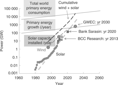
1.1 Growth in solar and wind energy installations per year, and the cumulative sum of wind and solar capacity (black curve), compared to global primary energy consumption and primary energy growth per year (thin solid grey lines at top of figure). Solar installations: historical and projected (small symbols) and long-term average trend (thick dashed line). Wind installations: historical and projected (large symbols and connecting curve), data from the Global Wind Energy Council. By 2030 solar will be the leading renewable energy source, providing a substantial fraction of global primary energy.
The dominant contributor to PV energy generation capacity, at present and for the foreseeable future, is silicon-based technology; in particular, crystalline (c-Si) and multicrystalline (mc-Si) silicon wafers that are integrated into solar panels. At present, silicon is the only semiconducting material that can clearly sustain the growth of PV into the range of terawatts per year, as needed to make a substantial contribution to global energy use. Although current technologies for fabricating self-supporting silicon wafers, and perhaps even the wafers themselves, may be obsolete by that time, new methods of producing highly efficient yet cheap silicon PV can be foreseen. These will avoid the material-related limitations of other technologies (e.g. the scarcity of In for CIGS solar cells and Te for CdTe cells, or the high costs of recycling toxic metals (e.g. Cd from CdTe-based solar cells).
This chapter reviews the current status of wafer-based silicon PV and explores likely future developments, including technologies enabling combined cost reduction and efficiency enhancement. The sections are organised along the lines of the industry supply chain shown in Fig. 1.2: starting with polysilicon production, then crystallisation, wafering and solar cell fabrication.
1.2 Polysilicon production
The first step in producing silicon suitable for solar cells is the conversion of high-purity silica sand to silicon via the reaction SiO2 + 2 C → Si + 2 CO, which takes place in a furnace at temperatures above 1900°C, the carbon being supplied usually in the form of coke and the mixture kept rich in SiO2 to help suppress formation of SiC. Further chemistry is undertaken to fully eliminate SiC from the product. Most of the resultant ‘metallurgical grade’ (MG) silicon is used for aluminium casting or in the chemical industry. The remainder (currently only a few per cent, but rising rapidly) is further refined in order to manufacture solar cells. An almost negligible proportion (despite the importance of the final product) goes to fabrication of wafers for the electronics industry. In the medium to long term, the rapid and sustained expansion of the PV industry may make it the largest consumer of metallurgical grade silicon. The trends outlined earlier are quantified in Fig. 1.3.
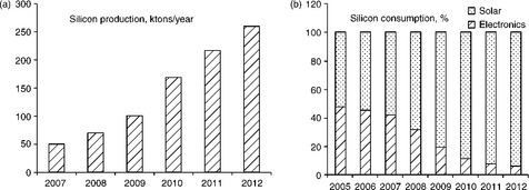
1.3 (a) Growth in annual polysilicon production in kilotons. Bars show growth prediction made in 2008 (Fishman, 2008); (b) the solar industry (dark grey) has taken over from electronics as the primary consumer of polysilicon. (Data from SEMI, April 2012.)
After production of MG silicon, the next step in producing material suitable for solar cells is purification, typically by a factor of 106−109. In the past this has been done by the Siemens process, originally developed to produce very high purity silicon for the electronics industry. Although energy, material and potential pollution costs are high, this process has been adapted for production of solar grade silicon, and modifications have been introduced to reduce costs and minimise undesired by-products at the much larger manufacturing scales required by the solar industry.
1.2.1 Siemens process
The Siemens process involves three main steps. First, Si is converted to ‘trichlorosilane’ (TCS) in a fluidised-bed reactor (FBR) through the reaction Si + 3HCl → SiHCl3 + H2. This removes most impurities but further purification is still required. Second, the TCS, which boils at 32°C, is distilled in order to reach the required purity. Third, the TCS is broken down in a reducing atmosphere at around 1000°C via the reaction SiHCl3 + H2 →Si + 3 HCl, so that Si atoms from the vapour are deposited on a silicon starting ‘seed’, usually consisting of a cylindrically arranged array of thin Si rods. This ‘chemical vapour deposition’ (CVD) process produces thick rods of highly pure silicon. Dopants such as B, P or As at the required concentrations to produce p-type (B) or n-type (As, P) solar cells are introduced by parallel reactions involving B2H6, AsH3 or PH3. After deposition the rods are removed from the reactor and broken into small polysilicon pieces - the starting material for growth of large single crystal or multi-crystalline blocks that will subsequently be cut into wafers.
It is a severe challenge for the Siemens process to continue meeting the scale and cost reduction requirements of the solar industry. Key problems are the incomplete utilisation of TCS and the formation of large volumes of potentially toxic by-products that require recycling, destruction or storage. This is a critical issue given the manufacturing scales involved.
1.2.2 Modified Siemens process
In the modified Siemens process, additional processing involving several stages (pressure condensation, adsorption, desorption) is used to separate the toxic, corrosive ‘tail’ gas from the TCS reduction process into its constituents (H2, HCl, SiCl4, SiHCl3, SiH2Cl2). As outlined in Fig. 1.4, most of these (H2, HCl and SiHCl3) are then directly re-used in the primary process, while SiCl4 undergoes an additional hydrogenation step to form TCS which is then also re-used. Despite these improvements, the modified Siemens process remains a batch process. Scaling and cost issues suggest that continuous production methods will eventually come to dominate polysilicon manufacturing.
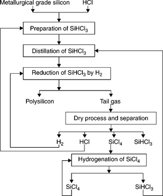
1.4 Flow diagram of the modified Siemens process. (Source: Papay, 2010. Reprinted with permission from the National Academies Press, Copyright 2010, National Academy of Sciences.)
1.2.3 Fluidised bed process
In this approach the pyrolysis of Si-containing gas to form polysilicon (as in the third step of the Siemens process) is achieved in a continuous and less energy-intensive way. Silane (SiH4) is introduced into a FBR together with a carrier gas (typically H) and heated to dissociate the SiH4. Polysilicon seed particles, a few tenths of a mm in size, are introduced continuously with the gas. Deposition of Si from the gas phase onto these particles leads to growth of larger polycrystalline granules that sink to the bottom of the reactor and can be extracted during continuous operation. The carrier gas dilutes the reactive SiH4, ensuring that deposition on seed particles dominates over homogeneous nucleation in the gas phase. This is important because homogeneous nucleation produces very small particles, ‘fines’, which may deposit on reactor surfaces, reducing reactor lifetime, and are less convenient than polysilicon granules as a starting material for Si crystal manufacture. Currently FBR technology contributes only a small fraction of the polysilicon produced worldwide, with a significant learning curve ahead. Continuing research and development is likely to increase its role and enable significant further polysilicon cost reductions in future.
1.3 Crystallisation and wafering
In this stage of silicon wafer production, polysilicon is melted and recrystallised into single-crystal or multicrystalline silicon, either in the form of large ingots which must be cut into wafers, or directly into wafers. This section describes the two main approaches used in the solar industry – pulling a crystal from a melt and directional solidification.
1.3.1 Single-crystal growth by the Czochralski method
The Czochralski process is currently the main route to fabrication of single- crystal silicon for both the microelectronics and solar PV industries. Its original discovery is said to have occurred when Jan Czochralski sat writing with a pen, inkwell and a crucible of molten tin nearby. By mistake, Czochralski dipped his pen into the tin and noticed a thin fibre of metal had grown from the slot in the pen nib. He later found that the fibre was a single crystal, and invented similar processes (using capillaries or single-crystal seeds) to grow various metals in single-crystal form. The Czochralski growth of germanium and silicon, introduced by Teal and Little at Bell Labs in the late 1940s and the early 1950s, provided the essential material for the transistor and the microelectronics industry that developed over the following 60 years.
In the Czochralski process for silicon a high-purity silica crucible is filled with polysilicon pieces or granules with the desired doping level. The crucible is held in a susceptor surrounded by heating elements and insulation, and Ar gas flows around the crucible, providing an inert atmosphere, creating an even temperature distribution and carrying away SiO gas – which has originated from the crucible – from the surface of the silicon melt. A crystal seed is dipped into the melt, is initially pulled up quite rapidly to narrow the growing crystal, eliminating grain boundaries to form a single grain, and then more slowly so that the crystal widens to the full diameter that will be required for wafer fabrication.
As the crystal is pulled, it is rotated to maintain uniformity of temperature, growth rate and doping, while the crucible rotates in the opposite sense. The temperature distribution and the rate of rotation and pulling of the wafer are all critical parameters of commercial importance. Owing to impurity segregation, oxygen, dopants and most other impurities have a higher concentration in the melt than in the crystal. Consequently, as the growth proceeds and the melt volume decreases, the impurity concentration in the melt increases. This tends to produce higher impurity concentrations at the bottom end of the crystal. Growth parameters have to be adjusted as far as possible to minimise this variation.
A significant issue with the p-type (normally boron doped) Cz silicon used in most single-crystal solar cells is the high O concentration in the silicon, which leads to light-induced degradation of conversion efficiency due to formation of a deep-level B–O complex activated by excess carriers (Voronkov et al., 2011). O incorporation in Cz silicon occurs as a result of convective transport of O in the melt, driven by the rotation of the crystal and thermal gradients. By applying a high magnetic field to the melt, convection can be significantly reduced, thus also reducing the O content of the grown crystal.
In a magnetic Czochralski process an external magnetic field is applied to stabilise convective oscillations in the melt, thus reducing growth inhomogeneities and the concentration of O incorporated in the crystal. Various magnetic configurations and time dependencies have been used: in Fig. 1.5 the temperature (left) and velocity distribution (right) in the melt are shown in the case of a static axisymmetric cusp field. The field strength increases from top to bottom of the sequence.
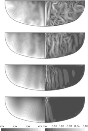
1.5 Temperature (left) and velocity (right) distributions in the melt during magnetic Czochralski growth using an axisymmetric cusp field. The magnetic field intensity increases towards the bottom of the sequence (Savolainen et al., 2002). (Source: Image reproduced with permission of CSC, IT Center for Science Ltd, copyright 2002.)
Czochralski growth produces cylindrically shaped silicon crystals (i.e. crystals with a circular cross-section) which are then sawn lengthways to produce either a pseudo-square cross-section with rounded corners or a square cross-section. The choice of cross-section reflects the manufacturer’s preferred trade-off between efficiency of silicon utilisation (favouring a rounded shape) and efficiency of light capture by the final solar panel (favouring square cells that can be abutted with minimal gaps).
1.3.2 Casting processes
Casting provides a higher throughput, less energy intensive and cheaper path to fabrication of solar grade silicon wafers. The material produced is multicrystalline, with a wide range of grain sizes depending on the technology used. High-throughput casting can be done by pouring liquid silicon from an upper crucible into a lower one in which the silicon solidifies slowly from the bottom of the crucible upwards. Technological improvements have enabled a nearly planar crystallisation front, thus reducing stresses and enabling formation of large grains in the range of cm (Schönecker et al., 2004). As in the Czochralski process, issues arise from segregation during growth, leading to variations in impurity concentrations in the grown ingot. Throughput of silicon ingot material is several times higher than for Cz silicon, and individual ingots now have masses approaching one tonne.
In conventional casting, crystallisation typically starts at a number of locations after the melt has cooled below the melting temperature, leading to formation of multiple grains that elongate during solidification (dendritic growth). Significant improvements are possible by introducing seed crystals. This approach has been developed relatively recently for large-scale casting – a seed, possibly a Cz silicon slice, is placed at the bottom of the solidification crucible, enabling rapid epitaxial crystallisation to form a quasi monocrystalline ingot with well-controlled crystallographic orientation over most of its volume, except close to the ingot base and sides (Fig. 1.6). This ‘quasi-mono’ technology appears to offer important advantages. Efficiency of cells made from material from most of the volume of the ingot approaches that of single-crystal silicon wafers. Moreover, square-section bricks (and subsequently square wafers) can be cut more efficiently from an ingot, providing nearly 100% area coverage when mounted on solar panels. This is an efficiency advantage over pseudo-square monocrystalline wafers which leave gaps, and a cost advantage over square-cut mono wafers whose manufacture requires large volumes of high-quality silicon to be reprocessed. Finally, the absence of grain boundaries in all but the edges of the ingot volume allows metal impurities to segregate more effectively out of the crystal, instead of becoming trapped at grain boundaries and re-entering the crystal during cell processing.
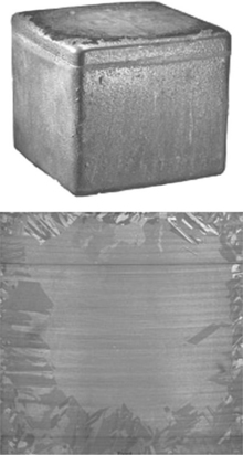
1.6 A 14 kgingot fabricated by seeded growth. The slice (bottom) shows multicrystalline structure at the edge of the block and a single crystal in the central portion of the ingot volume. In larger ingots the single crystal volume considerably exceeds the multicrystalline part. Image reproduced with permission of Dr Benoit Marie (Marie et al., 2011).
Residual efficiency limitations of quasi-mono material with respect to Czochralski wafers may arise from the presence of multicrystalline areas near ingot edges (limiting the fraction of the ingot that will yield premium material), and from dislocations formed during the directional solidification process (Marie, 2011; Tachibana et al., 2011), which may make it more difficult to getter metal impurities during cell processing. On the other hand, the low O content of quasi-mono silicon compared to Cz silicon suggests that it may produce higher efficiency cells at lower cost than Cz silicon, once the technology has been fully developed. At the time of writing, the manufacture and use of quasi-mono wafers is growing rapidly and this technology has the potential to take significant market share.
Seed crystals are also used in some growth methods for direct fabrication of solar wafers. For example, a thin silicon crystal seed between two wires can be used to lift a solid silicon film from a meniscus of molten silicon. However, currently the efficiencies of cells fabricated in such wafers are significantly lower than those of cells made from sawn wafers – probably as a result of defects and impurities arising from the presence of nearby interfaces. 1366 Technologies claims to be about to build a commercial manufacturing facility using a ‘moulding’ process to directly fabricate crystalline silicon solar wafers (Technology Review, 2012).
1.3.3 Doping
The choice of dopant element during crystal growth, either p-type (boron, B or gallium, Ga) or n-type (phosphorus, P) depends on a number of factors. Traditionally p-type doping has been used, using B as it has a segregation coefficient close to unity, making it easier to obtain uniform doping in batch Czochralski or casting processes that consume the liquid phase. P-type doping also allows the use of simple processing steps during cell manufacture: POCl3 for emitter formation and silicon nitride for passivation. This however introduces problems with light-induced degradation, as B interacts with O in the wafer to form deep-level recombination centres. One solution to this is the use of Ga doping in place of B. This can be problematic as Ga has a very low segregation coefficient, below 0.01 (Coletti et al., 2011), however the introduction of continuous Czochralski (CCz) growth makes it possible to consider this option (Ciszek, 2011).
Another solution is to switch to n-type silicon (Glunz et al., 2010), again, using the CCz method. In this case the emitter doping in subsequently manufactured cells has to be p-type, leading to the use of more expensive boron implanted emitters to obtain sufficiently high doping levels, as boron has a lower electrical solubility than phosphorus in crystalline silicon (Hermle et al., 2011; Hielsmair et al., 2011; Pawlak et al., 2012). Moreover, for the majority of n-type cell technologies, which use dielectric passivation, the dielectric material has to be changed so that the polarity of interface charges is of the right sign to repel minority carriers. This has led to the introduction of alumina, deposited by chemical vapour deposition or atomic-layer deposition (Richter et al., 2010; Dingemans et al., 2011; Werner et al., 2011), as a replacement for silicon nitride for emitter passivation.
1.3.4 Impurities
Numerous impurity species in silicon have detrimental effects on solar cell performance, even at very low concentrations, as they introduce deep-level centres that allow recombination of charge carriers within the bulk silicon material. Iron is a particular problem, as interstitial iron is a strong recombination centre and can be present at significant concentrations, especially in cast silicon (Carberry et al., 2011). Other significant low-concentration impurities are Cr and Au. Significant high-concentration impurities are O (in combination with boron) and C.
Metal impurities are typically distributed between interstitial positions within the crystal lattice, and positions at dislocations, grain boundaries and precipitates. The latter sites have significant binding energies, making it more difficult to ‘getter’ the metal from the material. On the other hand, the recombination efficiency of impurities is significantly reduced by precipitation (Istratov et al., 2003).
Gettering of iron and other fast-diffusing metals is done during wafer processing. Phosphorus diffusion gettering occurs during cool-down from high-temperature diffusion steps during processing of cells on p-type wafers, where highly doped phosphorus is present in the emitter. However, the move to selective emitters (SEs) and more lightly doped shallow emitters for blue sensitivity significantly reduces the active gettering area. Aluminium gettering occurs during traditional aluminium back surface field formation and subsequent thermal treatment, as impurities segregate preferentially into the Al–Si alloy used. However, again, replacement of this process with local back contacts, sometimes even ion-implanted, eliminates this gettering process. This places additional emphasis on cleaning up the starting material, including reducing the density of dislocations, which trap impurities, and on applying novel methods such as intrinsic gettering.
Deep-level defects in the crystal lattice, at dislocations and at grain boundaries can be passivated to a large extent by annealing in hydrogen. At defects and grain boundaries the defect level may remain but move towards the band edge, where it is less effective in promoting recombination (Martinuzzi et al., 2003).
1.3.5 Wafering
Czochralski-grown crystals are converted into wafers by sawing with steel wire, using slurry, or with diamond-coated wire. Ingots, which are larger, are first sawn into ‘bricks’ – these are subsequently sawn into wafers. Key issues driving the use of diamond wire are the need to reduce kerf loss (silicon removed in the cutting process), increase cutting speed and reduce down time for saw replacement. This is a major issue, as the thickness of wafers used in manufacturing is expected to decrease to below 150 ^m within the next few years. After cutting, wafers are etched to remove ‘saw damage’ – impurities and dislocations introduced by sawing. This involves removing a few micrometres of each side of the wafer, usually as part of a wafer texturing process step. The wafer is then ready for further processing into a solar cell.
1.4 Solar cells: materials issues and cell architectures
Solar cells have developed considerably during several decades of research and development, however, it is only relatively recently that many of these developments have begun to appear in manufactured cells as commercial competition based on the conversion efficiency of cells and panels has become more important. This section describes some of the important developments. For more detailed discussions the reader is referred to recent literature (Saga, 2010 and references therein; Green, 2011 and references therein; Glunz, 2007); and a standard reference book (Green, 2008).
1.4.1 Standard cell
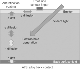
The workhorse of currently manufactured silicon wafer-based PV is a simple quasi one-dimensional diode structure approximately 175 µ thick, with an n-type phosphorus-diffused emitter on the sun side (top side), uniform p-type doping in the bulk of the wafer and a more heavily doped p-type ‘back surface field’ in the last few microns of the wafer, close to the back side (Fig. 1.7). The back surface field, usually consisting of aluminium- doped silicon generated by thermal processing of the aluminium-deposited or screen-printed back contact, prevents minority carriers (here, electrons) from entering the back contact. Including a proportion of boron in the aluminium back contact allows higher and steeper doping in the back surface field, which may be beneficial in reducing contact recombination losses (Lölgen et al., 1994). This would especially apply in the case of thin deposited aluminium contacts. The front side is passivated with silicon nitride or silicon dioxide and in either case silicon nitride (added as a top layer in the case of oxide passivation) is used as an antireflection coating. Metal fingers, usually deposited as screen-printed paste and then fired through the nitride layer, are used to collect electron current from the emitter, while an aluminium back contact collects holes arriving through the back surface field. Typically two or three ‘busbars’ (thicker metal lines oriented perpendicular to the fingers) collect the current arriving from each finger and pass it to tags at the edge of the cell for connection to the next cell in the panel. Prior to fabrication the wafer is textured (usually by a KOH or acid etch) to improve light capture, hence the name ‘black cell’ (Haynos et al., 1974). The process is low- cost, but the cell is also of low efficiency, relying on technology developed in the 1970s and 1980s. Material costs are quite high as the paste contains silver, and the PV industry, currently the largest industrial user of the metal, is driving up its price. Silicon consumption is high because wafers need to be relatively thick compared to current trends: standard cells thinner than 200 μm are significantly less efficient due to absorption of red/near-infrared light at the back contact, which is a poor reflector.
1.4.2 Improvements to the standard cell
Over several decades numerous improvements to the standard cell have been introduced in research and development, and several are now being implemented by the mainstream PV industry following their introduction by market leaders. Two notable improvements are the use of SEs and the use of local back contacts.
In the SE approach, the region under the fingers is heavily doped to reduce the contact resistance to the finger, while the doping of the main part of the emitter, through which light passes as it enters the cell, is reduced to enhance the blue sensitivity of the cell.
Methods such as local laser doping are a convenient approach to produce SEs (Granek et al., 2011; Hirata et al., 2011). The SE approach typically produces a roughly 1% enhancement of cell efficiency.
A specialised version of the SE approach is the laser-grooved buriedcontact (LGBC) cell originally developed by BP Solar, now manufactured by Narec Solar. This cell structure is shown schematically in Fig. 1.8.
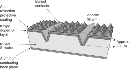
1.8 Schematic of the laser-grooved buried contact (LGBC) cell. This structure gives the advantage of less shadowing from the front side fingers, due to their high aspect ratio. (Image reproduced with permission of Dr Alex Cole, Narec Solar.)
The selective emitter region is created after emitter formation and front-side passivation/antireflection coating, by laser-cutting a narrow contact groove through the coating and into the silicon. The groove is then heavily doped with phosphorus, using POCl3 doping in a diffusion furnace, and filled by electroless plating. The LGBC has potential for high efficiency when combined with other enhancements, and offers specialist advantages for low- and medium-concentrator cells where the pitch has to be smaller than in standard cells because of the high current density.
Local back contacts provide a significant improvement as most of the back side is covered by a passivating dielectric, rather than by the back contact, thus strongly reducing recombination. Thermally grown silicon dioxide provides good-quality passivation and can be covered by silicon nitride for improved optical reflection. This further allows the use of thinner wafers without loss of cell efficiency. Metal contacts are fired through the back side dielectric or plated through contact holes. Their size is optimised to minimise recombination at contacts but avoid issues with current crowding. Plate I (see colour section between pages 238 and 239) shows a device simulation of the current flow in a local back contacted cell.

Plate I Device simulation of a solar cell with local back contacts. The streamtrace plot shows the current flow between front contact finger (top left) and back contact (bottom centre). The simulation cell dimension (L×H×W) is 500 μm × 150 μm × 350 μm. Image courtesy of V. Moroz, Synopsys.
N-type contact regions can also be passivated using sub-nanometre tunnelling dielectric deposited by atomic layer deposition (Zielke et al., 2011).
To overcome the high cost of silver, manufacturers are moving on from screen printing of thick paste layers to plating techniques (Kray et al., 2011). An overview of this transition has been given by Green (2011).
1.4.3 Advanced cell architectures
Recently various new architectures have been introduced which enhance efficiency by a combination of improved light trapping and improved carrier collection. All are inherently three-dimensional, at least with respect to carrier collection. In the interdigitated back contact (IBC) cell, shown in Fig. 1.9, the current flows predominantly laterally along curved paths towards alternating n-type and p-type contact regions in an approximately common plane at the back side of the wafer. This arrangement has important advantages: there is no shadowing, so light trapping efficiency is high, and the back contact arrangement allows rapid assembly into panels using surface mounting technology. The efficiency potential of this type of cell is around 25%.
1.9 Schematic cross-section of an interdigitated back contact solar cell. For simplicity, texture is not shown.
In the IBC cell the length of the current path is controlled by the lateral pitch of the interdigitated contacts and the thickness of the wafer, the dominant contribution coming from the pitch. This creates a requirement for longer diffusion lengths (higher material quality) in order to avoid degradation of efficiency as a result of increased bulk recombination, thus IBC cells usually use relatively expensive n-type single-crystal silicon. It also motivates the use of more advanced contacting and patterning methods that will allow a smaller pitch, for example, inkjet printing and contact plating in place of screen printing (Baert et al., 2011), and ultimately also thinner wafers.
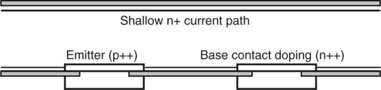
Two further cell types are the emitter wrap-through (EWT) cell and the metal wrap-through (MWT) cell. In the EWT cell a lightly doped emitter on the top side of the wafer is connected to an emitter contact region at the back side through holes, or vias, cut through the wafer, usually by laser cutting. The vias are doped at the same time as the emitter to provide a current path for carriers collected at the front side to reach the back side emitter contact. Base contacts with back surface field doping are interspersed between the emitter contacts, with dielectric passivation between the contacts. Plate II shows current distributions in a simplified model of an EWT cell element including one via. The EWT cell has the same relatively short current path to the emitter junction as in the standard cell, and therefore has standard requirements for material quality, thus tending to make it a cheaper option than the IBC cell.
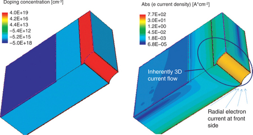
Plate II Device simulation of an emitter wrap-through solar cell, flipped over to show the back contact regions. At left, the doping distribution in the silicon, showing back-surface field doping in the base contact region (dark blue) and emitter doping along the via and in the back-side emitter contact region (red). At right, the electron current distribution in the cell.
In the MWT cell, current flow through the vias is supported by filling the holes with contact metal. This improves the fill factor of the cell, enables a wider spacing between via holes, and also enables better optimisation of emitter doping parameters for improved carrier collection and light capture. Variants of the MWT cell include a standard form in which regular metal fingers, but no busbars, are present on the front side, and modified forms in which the fingers have more complex geometry, or are omitted in favour of increased light capture traded against poorer carrier collection. The MWT cell may be the most suitable of the new cell types for widespread manufacturing in the near future, as it is reasonably compatible with standard cell processing.
Finally, the use of amorphous/crystalline silicon heterojunctions, originally pioneered by Sanyo, is now being explored in a variety of architectures with the aim of reaching efficiencies approaching 25% (Kinoshita, 2011).
Silicon solar cells are likely to enter a new phase of research and development of techniques to enhance light trapping, especially at oblique angles of incidence encountered with fixed mounted (e.g. rooftop) panels, where the efficiency of panels that rely on surface texturing of cells can drop to very low values. Efficiency improvements under oblique-angle incidence are possible using texturing of glass front sheets (EMMVEE, 2011), and greater improvements at a more fundamental engineering level may be possible by creating fully three-dimensional (3D) optical structures integrated within the cell (Solar3D, 2012).
Developments further in the future (with respect to crystalline silicon cells) are likely to include multijunction cells (Luque, 2011), using higher band-gap semiconductors on silicon cell substrates, high-efficiency directly fabricated crystalline silicon wafers, and better crystallisation and passivation methods for thin crystalline silicon films on foreign substrates.
1.5 Conclusions
Silicon PV currently dominates the global market for solar generated electricity. The pace of expansion is essentially limited by the pace of innovation and financing, since it is already clear that silicon PV will scale up to the multiple-terawatt level required for conversion from fossil fuel to renewable energy.
Cost reduction and efficiency enhancement are key issues for accelerating the expansion of solar PV. Current and near-future developments have potential to shorten the silicon PV industry supply chain. Wafers may be directly cast instead of being cut from large grown ingots, or may be entirely superseded by crystallising silicon on foreign substrates. Continuing innovations that allow down-scaling of silicon thickness and emitter–base contact separation will enable use of cheaper and less silicon material, less energy consumption in manufacturing, and will lead to increased conversion efficiency.
With this perspective in mind there is every confidence that ‘Moore’s Law’ will continue to apply to the growth of silicon PV, almost certainly allowing a full transition to renewable energy by the 2030s.
1.6 References
Baert, K., Dross, F., Gordon, I., Horzel, J., John, J., Posthuma, N.E., Mertens, P., Mertens, R., Poortmans, J., Crystalline silicon solar cells: where microelectronics meets photovoltaics. photovoltaicsProceedings of 26th European Solar Photovoltaics Conference, 2011.
Branker, K., Pathak, M.J.M., Pearce, J.M. A review of solar photovoltaic levelized cost of electricity. Renewable and Sustainable Energy Reviews. 2011; 15:4470–4482.
Black, L.E., Provancha, K.M., McIntosh, K.R., Surface passivation of crystalline silicon by APCVD aluminium oxide. Proceedings of 26th European Photovoltaic Solar Energy Conference, 2011. [Hamburg, Germany].
Carberry, J.J. Method of making a solar grade wafer, 2009. [US Patent 7,604,696, issued to John J Carberry, 20 October 2009.].
Carberry, J.J., Wereszczak, A., Skumanich, A., Mitigating impurity levels in crystal growth for c-Si: Implications for improved cell efficiencies and lower $/W production. Proceedings of 26th European Solar Photovoltaics Conference, 2011. [Hamburg, Germany].
Ciszek, T.F., Wang, T.H., Page, M.R., Landry, M.D., Bauer, R.E. Silicon materials research on growth processes, impurities, and defects. 2003 NREL report NREL/ CP-520-33575.
Coletti, G., Macdonald, D., Yang, D. Role of impurities in solar silicon. In: Pizzini S., ed. Advanced silicon materials for photovoltaic applications. Wiley, 2011.
Dingemans, G., Terlinde, N.M., Verheijen, M.A., van de Sanden, M.C.M., Kessels, W.M.M. Controlling the fixed charge and passivation properties of Si(100)/ Al2O3 interfaces using ultrathin SiO2 interlayers synthesized by atomic layer deposition. Journal of Applied Physics. 2011; 110:093715.
EMMVEE Photovoltaics, More efficiency with structured glass, 2011. http://www.emmveephotovoltaics.com/english/press/archive [Press release, URL, (accessed 22 March 2012)].
Glunz, S.W., High efficiency crystalline silicon solar cellsAberle, A., eds. Recent advances in solar cells; vol. 2007, 2007 special issue, Advances in OptoElectronics
Glunz, S.W., Benick, J., Biro, D., Bivour, M., Hermle, M., Pysch, D., Rauer, M., Reichel, C., Richter, A., Rüdiger, M., Schmiga, C., Suwito, D., Wolf, A., Preu, R., n-type silicon – enabling efficiencies > 20% in industrial production. Proceedings of 35th Photovoltaic Specialists Conference, 2010. [Honolulu, Hawaii].
Granek, F., Hopman, S., Kluska, S., Fell, A., Breitwieser, M., Fleischman, C., Glatthaar, M., Glunz, S.W., et al, Progress in laser chemical processing for silicon solar cells. Proceedings of 26th European Solar Photovoltaics Conference, 2011. [Hamburg, Germany].
Green, M.A., Quo vadis silicon photovoltaics. Proceedings of 26th European Photovoltaic Solar Energy Conference, 2011. [Hamburg, Germany].
Green, M.A. High efficiency silicon solar cells. Aedermannsdorf, Switzerland: Trans Tech Publications; 2008.
Haynos, J., Allison, J., Arndt, R., Meulenberg, A., The COMSAT non-reflective silicon solar cell: a second generation improved cell. Proceedings of International Conference on Photovoltaic Power Generation, 1974:487. [Hamburg, Germany].
Hermle, M., Benick, J., Rudiger, M., Bateman, N., Glunz, S.W., N-type silicon solar cells with implanted emitter. Proceedings of 26th European Solar Photovoltaics Conference, 2011. [Hamburg, Germany].
Hielsmair, H., Mandrell, L., Chun, M., Latchford, I., Adibi, B., Advantages of ion-implantation for solar cells. Proceedings of 26th European Solar Photovoltaics Conference, 2011. [Hamburg, Germany].
Hirata, K., Takayama, T., Hasegawa, M., Funatani, T., Fuyuki, T., Optimization of selective emitter formation using laser doping in crystalline silicon solar cell. Proceedings of 26th European Solar Photovoltaics Conference, 2011. [Hamburg, Germany].
Istratov, A.A., Buonassisi, T., McDonald, R.J., Smith, A.R., Schindler, R., Rand, J.A., Kalejs, J.P., Weber, E.R. Metal content of multicrystalline silicon for solar cells and its impact on minority carrier diffusion length. Journal of Applied Physics. 2003; 94:6552–6559.
Kinoshita, T., The approaches for high efficiency HITTM solar cell with very thin (< 100 μm) silicon wafer over 23%. Proceedings of 26th European Solar Photovoltaics Conference, 2011. [Hamburg, Germany].
Kray, D., Bay, N., Cimiotti, G., Fritz, N., Glatthaar, M., Kleinschmidt, S., Lösel, A., Lühn, O., Schramm-Moura, J., Rodolfili, A., Träger, A., Kuehnlein, H., Nussbaumer, H., Reducing Ag cost and increasing efficiency. Multicrystalline silicon solar cells with direct plated contacts exceeding 17% efficiency. Proceedings of 26th European Solar Photovoltaics Conference, 2011. [Hamburg, Germany].
Lölgen, P., Sinke, W.C., Leguijt, C., Weeber, A.W., Alkemade, P.F.A., Verhoef, L.A. Boron doping of silicon using coalloying with aluminium. Applied Physics Letters. 1994; 65:2792–2794.
Luque, A. Will we exceed 50% efficiency in photovoltaics? Journal of Applied Physics. 2011; 110:031301.
Marie, B., Bailly, S., Jouini, A., Ponthenier, D., Plassat, N., Dubost, L., Pihan, E., Enjalbert, N., Garandet, J.-P., Camel, D., Seeded grown mono-like Si ingots: effect on recombination activity of dislocations. Proceedings of 26th European Solar Photovoltaics Conference, 2011. [Hamburg, Germany].
Martinuzzi, S., Périchaud, I., Warchol, F. Hydrogen passivation of defects in multicrystalline silicon solar cells. Solar Energy Materials & Solar Cells. 2003; 80:343–353.
Moore, G.E. Cramming more components onto integrated circuits. Electronics. 1965; 38:114–117.
Papay, L., Committee on U.S.-China Cooperation on Electricity from Renewable Resources, National Academy of Engineering and National Research Council of the US National Academies, Chinese Academy of Sciences and Chinese Academy of Engineering, The power of renewables: opportunities and challenges for China and the United States, Washington, DC: National Academies Press; 2010, 978-0-309-16000-1.
Pawlak, B.J., Janssens, T., Singh, S., Kuzma-Filipek, I., Robbelein, J., Posthuma, N.E., Poortmans, J., Cristiano, F., Bazizi, E.M. Studies of implanted boron emitters for solar cell applications. Progress in Photovoltaics. 2012; 20:106–110.
Richter, A., Hörtels, M., Benick, J., Heneck, S., Hermle, M., Glunz, S.W., Towards industrially feasible high-efficiency n-type Si solar cells with boron-diffused front-side emitter – combining firing stable Al2O3 passivation and fine-line printing. Proceedings of 35th Photovoltaic Specialists Conference, 2010. [Honolulu, Hawaii].
Saga, T. Advances in crystalline silicon solar cell technology for industrial mass production. NPG Asia Materials. 2010; 2:96–102.
Savolainen, V., Heikonen, J., Ruokolainen, J., Anttila, O., Laakso, M., Paloheimo, J. Simulation of large-scale silicon melt flow in magnetic Czochralski growth. Journal of Crystal Growth. 2002; 243:243–260.
Schönecker, A., Geerligs, L.J., Müller, A. Casting technologies for solar silicon wafers: block casting and ribbon-growth-on substrate. Solid State Phenomena. 2004; 95–96:149–158.
Solar3D, Solar3D high efficiency solar cell fits into highest growing segment, 2012. http://www.solar3d.com/index.php
Stoddard, N., Wu, B., Witting, I., Wagener, M., Park, Y., Rozgonyi, G., Clark, R. Casting single crystal silicon: Novel defect profiles from BP Solar’s Mono2 ™ wafers. Solid State Phenomena. 2008; 131–133:1–8.
Tachibana, T., Sameshima, T., Miyazaki, N., Kojima, T., Arafune, K., Kakimoto, K., Miyamura, Y., Harada, H., Sekiguchi, T., Ohshita, Y., Ogura, A., Evaluation of crystalline defects in silicon ingots fabricated by seeding cast growth. Proceedings of 26th European Solar Photovoltaics Conference, 2011. [Hamburg, Germany].
Technology Review, Company profile: 1366 Technologies. Technology Review, MIT. 2012. http://www.technologyreview.com/tr50/1366tech/
Voronkov, V.V., Falster, R., Bothe, K., Lim, B., Schmidt, J. Lifetime-degrading boron-oxygen centres in p-type and n-type compensated silicon. Journal of Applied Physics. 2011; 110:063515.
Werner, F., Veith, B., Zielke, D., Kühnemund, L., Tegenkamp, C., Seibt, M., Brendel, R., Schmidt, J. Electronic and chemical properties of the c-Si/Al2O3 interface. Journal of Applied Physics. 2011; 109:113701.
Zielke, D., Petermann, J.H., Werner, F., Veith, B., Brendel, R., Schmidt, J., 21.7 % efficient PERC solar cells with AlOx tunneling layer. Proceedings of 26th European Solar Photovoltaics Conference, 2011. [Hamburg, Germany].