
Chapter 10: Discrete Light Propagation in Arrays of Liquid Crystalline Waveguides
Warsaw University of Technology, Warsaw, Poland
Nonlinear Optics and OptoElectronics Lab, University ROMA TRE, Rome, Italy
Warsaw University of Technology, Warsaw, Poland
10.1 Introduction
In the past two decades, linear and nonlinear effects in discrete systems, in the form of photonic structures with a periodic modulation of refractive index (along one or more spatial directions), have become the subject of growing interest. The latter mainly stems from both the inherent physics and the variety of potential applications [1–3]. The unique properties of discrete structures originate from the discretization of light–matter interactions (both in linear and nonlinear regimes) taking place over a finite number of unit elements in a photonic lattice. The relevance of discrete systems has been supported by a wealth of materials and nonlinear mechanisms to be employed, including semiconductors [4–6], glasses [7, 8], polymers [9], photorefractives [10, 11], ferroelectrics [12], with a cubic and a quadratic nonlinear response, respectively. This has resulted in a wide range of novel and fascinating phenomena such as discrete blockers and routers [13], discrete diffraction and solitons [1, 14–21], gap solitons [22], discrete breathers [23], multiband solitons and their interactions [24, 25], linear and nonlinear Bloch oscillations (BO) [26–30], Landau–Zener (LZ) tunneling [30–33], and several other effects that have been successfully demonstrated. At the same time, some peculiar properties arising from lack of rotational symmetry in discrete systems have been pointed out toward all-optical switching and signal readdressing [9, 13, 15, 16, 34, 35].
Besides the solid-state materials mentioned earlier, a great deal of attention has been devoted to waveguide arrays in nematic liquid crystals (NLCs). The latter, together with those arrays fabricated in photorefractives [10, 11] and droplet arrays in Bose–Einstein condensates [36], represent an excellent example of systems with a tunable discreteness, that is, lattices where period, index contrast, and/or nonlinearity can be effectively adjusted. Moreover, NLCs, in addition to their peculiar optical properties (including huge birefringence and extended spectral transparency), have been proven to be excellent dielectrics for nonlinear optics. Their giant nonresonant reorientational nonlinearity results in low power requirements for spatial light localization, supporting spatial solitons in both one and two dimensions [37–42] as well as discrete solitons [42–47]. In addition, the significant electro-optic response of NLC allows for the creation of flexible and voltage-tunable architectures [43, 46–48], including those specifically designed for discrete optical phenomena. Using one-dimensional waveguide arrays in NLC, it is possible to observe the transition from discrete diffraction to spatial light localization, as well as all-optical signal switching and angular steering. As reviewed in this chapter, discrete diffraction and discrete solitons [42–47, 49], nonlinear angular steering [50], multiband vector breathers [51], LZ tunneling [52–54], and BO [55] have been investigated in voltage-tunable NLC-based discrete arrays for near-infrared (IR) light.
This chapter is organized as follows: after a brief generic description of discrete light propagation in one-dimensional photonic lattices (Section 10.2), we discuss the realization of such structures in NLC (Section 10.3); then we present various discrete optical phenomena in NLC waveguide arrays (Sections 10.4–10.8).
10.2 Discrete Systems
Stemming from the pioneering work by Somekh et al. on linear light tunneling in a one-dimensional (1D) optical lattice [56], by Jensen on the nonlinear directional coupler [57], and by Christodoulides et al. on infinite arrays of identical waveguides [17], intensive studies on linear and nonlinear discrete light propagation in 1D waveguide arrays have been pursued considering various materials and nonlinearities. A photonic structure with a periodically modulated refractive index (Fig. 10.1a) is equivalent to an array of parallel channel waveguides. Light propagation in such an array of waveguides can be modeled as a multicore directional coupler, representing the electromagnetic field as a superposition of modes guided in individual channels. An effect of light tunneling between neighboring waveguides is the characteristic propagation pattern, known as discrete diffraction and shown in Figure 10.1b. This pattern is typical of a linear regime, that is, at low optical powers, when the excitation increases in a self-focusing nonlinear medium, the change in (effective) refractive index and the induced wave vector mismatch between input and adjacent channels prevents resonant tunneling across the array, progressively isolating the excited channel(s) from the neighboring ones and leading to light trapping and propagation within the launch waveguide(s). Eventually, at high enough power, a discrete soliton, that is, a spatially localized wave, can propagate along the lattice without diffraction or spreading (Fig. 10.1c). The generation of such localized state can be viewed as resulting from the balance between discrete diffraction (due to waveguide-to-waveguide coupling) and the power-dependent phase mismatch between adjacent waveguides.
Figure 10.1 (a) Example of refractive index distribution in a one-dimensional waveguide array. (b) Discrete diffraction. (c) Discrete spatial soliton in the presence of a power-dependent refractive index (self-focusing). (d) Beam propagation when launched at the zero-diffraction angle. (e) Negative discrete diffraction. (f) Dispersion diagram for a discrete system, with the relation between the propagation constants kz and kyΛ, with ky the transverse component of the wave vector (the Bloch wave number) and Λ the separation between waveguides (period of the refractive index modulation). Points A, B, C, and D correspond to the cases in panels (b), (c), (d), and (e), respectively.
Owing to their periodicity in the transverse direction, discrete systems are characterized by a unique relation between the propagation constant kz and the transverse component ky of the wave vector. It is convenient to introduce the diffraction coefficient ![]() , analogous to group velocity dispersion in dispersive media. The diffraction coefficient D can be zero in discrete systems at some excitation angles, that is, for some values of the transverse wave vector ky: under such conditions, the input beam propagates across the array in a nearly nondiffracting manner, as displayed in Figure 10.1d [58]. This feature, combined with the generation of discrete solitons with zero transverse velocity at high powers, allows implementing all-optical signal steering. It is also possible to obtain negative diffraction (with D < 0), as shown in Figure 10.1e. As in photonic crystals or in the case of electrons in periodic structures [59], a more accurate analysis requires the use of Bloch theory. The dispersion diagram (relating the propagation constant kz to the Bloch wave number ky) is composed of bands separated by gaps, wherein light propagation is forbidden (Fig. 10.1f). The study of modes in distinct bands together with the possibility of their interplay paves the way for the observation of gap solitons [22, 60], discrete breathers [23, 61], multiband vector solitons [24, 25, 51, 62, 63], and dynamic phenomena typical of quantum mechanical systems, including BO [26–30, 64] and LZ tunneling in “accelerated” lattices [30–33, 52–54].
, analogous to group velocity dispersion in dispersive media. The diffraction coefficient D can be zero in discrete systems at some excitation angles, that is, for some values of the transverse wave vector ky: under such conditions, the input beam propagates across the array in a nearly nondiffracting manner, as displayed in Figure 10.1d [58]. This feature, combined with the generation of discrete solitons with zero transverse velocity at high powers, allows implementing all-optical signal steering. It is also possible to obtain negative diffraction (with D < 0), as shown in Figure 10.1e. As in photonic crystals or in the case of electrons in periodic structures [59], a more accurate analysis requires the use of Bloch theory. The dispersion diagram (relating the propagation constant kz to the Bloch wave number ky) is composed of bands separated by gaps, wherein light propagation is forbidden (Fig. 10.1f). The study of modes in distinct bands together with the possibility of their interplay paves the way for the observation of gap solitons [22, 60], discrete breathers [23, 61], multiband vector solitons [24, 25, 51, 62, 63], and dynamic phenomena typical of quantum mechanical systems, including BO [26–30, 64] and LZ tunneling in “accelerated” lattices [30–33, 52–54].
10.3 Waveguide Arrays in Nematic Liquid Crystals
The realization of a waveguide array in NLC is possible owing to their electro-optic response, which permits to transform an NLC layer into a 1D electromagnetic lattice. In order to introduce the required spatial distribution of the refractive index, a planar thin cell with a periodic set of fingered electrodes is used. Applying a voltage, the structure can be tuned from a planar waveguide supporting light confinement in one dimension (planar guiding in the NLC layer) to bidimensional confinement in a 1D array of identical weakly coupled channel waveguides. In such a way, a 1D photonic lattice is formed in NLC with refractive index modulation created and controlled by an external (low-frequency) electric field.
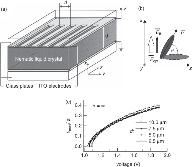
Figure 10.2 is a sketch of the structure. A thin (i.e., a few-micrometer thick) layer of the uniaxial NLC PCB (4′-n-pentyl-4-cyanobiphenyl) is sandwiched between two parallel glass plates, forming a standard planar waveguide with the NLC as the guiding layer. The thickness of the NLC layer is chosen in order to ensure transverse confinement along x in the absence of applied voltage (at the operating wavelength). The anchoring conditions imposed at the glass surfaces determine the planar alignment of the NLC within the cell, with the long axes of the molecules aligned along z, that is, along the direction of light propagation. The top glass plate is coated with a comb-shaped set of regularly spaced electrodes made of a 50 nm-thick transparent film of indium tin oxide (ITO), whereas the bottom one is uniformly covered by a grounded ITO film. The shape of the top electrode permits the application of a low-frequency (1 kHz) periodic voltage distribution [i.e., V(y) = V(y + Λ)] across the thickness d of the guiding NLC layer. It allows for the introduction of the spatially periodic refractive index modulation in NLC and leads to the formation of a one-dimensional dielectric lattice of constant period Λ. The lattice consists of identical channel waveguides providing light confinement in the transverse xy-plane and evanescently coupled to one another along y. In this chapter, we consider 50/50 duty cycle electrode patterns, that is, with equal finger widths and spacings. Samples with electrode periodicity ranging from 4 to 8 μm were tested experimentally, using NLC layer thicknesses up to a few micrometers in order to obtain evanescent-field coupling between channels (in the linear regime) and ensure a coupling length (millimeter scale) at the desired wavelength to be compatible with the experimental setup. This configuration provides considerable potentials for engineering the optical properties by tuning the sample parameters. As the confinement and the coupling strength of the bidimensional channel waveguides depend on the external bias, the main advantage of this structure is its voltage-controlled tunability, which, at variance with solid-state arrays, permits precise adjustments in both linear and nonlinear regime.
Figure 10.2 (a) Sketch of a one-dimensional NLC waveguide array with planar orientation. The top electrode is arranged in a periodic pattern of period Λ. (b) Sketch of the molecular reorientation (in the xz-plane) due to the electric field applied along x; the influence of low (Elf) and optical frequency (Eopt) fields may allow for periodic modulation of refractive index and nonlinear optical effects, respectively. (c) Maximum reorientation versus applied bias for several cell thicknesses in a sample with uniform electrodes: reorientation starts after a threshold voltage, that is, the Freedericksz transition.
In order to obtain a specific periodic distribution of refractive index within the NLC layer, a low-frequency field Elf is applied along x (Fig. 10.2b). In the ideal case of a planar configuration as considered here, the long axes of NLC molecules are uniformly oriented along z when no voltage is present. In NLCs with a positive low-frequency anisotropy, such as PCB with Δ ε lf = 11.5, the molecules tend to align their long axes (molecular director) along the external electric field (if the latter is above the Freedericksz threshold or in the presence of a small pretilt in xz), thereby changing the orientation angle θ (measured between z and the optic axis of uniaxial NLC) in xz and thus the optical properties of the NLC layer. Taking into account both electromagnetic and elastic forces and analyzing the total free energy [with term(s) depending on electric field(s) as well as terms describing the elastic contributions, as expressed through Frank's formalism], after its minimization, it is possible to obtain a differential (Euler–Lagrange) equation describing the relation between the orientation angle and the applied external field(s) (Chapter 1) [65, 66]. The low-frequency field distribution can be calculated from Maxwell's equations in the presence of the electric potential V. Through the fingered electrode, the periodic bias induces a spatial distribution of the effective refractive index for TM-like-polarized waves (i.e., with a dominant x-component of the electric field Eopt, see Figure 10.2b), given by ![]() , with no and ne being the ordinary and extraordinary NLC refractive indices, respectively.
, with no and ne being the ordinary and extraordinary NLC refractive indices, respectively.
The refractive indices of PCB [65–67] at room temperature and wavelength 1064 nm are 1.5158 (for ordinary polarization) and 1.6814 (for extraordinary polarization); they were used in all numerical simulations. At the same wavelength, the refractive index of BK7 glass is ng = 1.5066. In the single elastic constant approximation (i.e., equal for splay, bend, and twist deformations), the PCB elastic coefficient can be taken equal to K = 3.2 × 10⁻¹² N. Figure 10.3a shows an example of electric field distribution within the 5 μm-thick NLC film biased by comb electrodes with 6 − μm period. Figure 10.3c displays the resulting effective index distributions (for x-polarized light) in the xy-plane for three applied biases, whereas Figure 10.3b plots the results in the NLC midlayer, that is, for x = 0. The effective index increases more in the regions underneath the stripe electrodes, creating the channels and ensuring the lateral confinement of light. Moreover, Figure 10.3c demonstrates that a higher applied voltage induces a higher index modulation, provided the bias is low enough to avoid saturation effects; thus, the higher the bias the stronger is the light confinement.
Figure 10.3 (a) Electric field distribution in a d = 5 μm NLC layer for a voltage V = 1.35 V applied to the periodic electrode (Λ = 6 μm). Effective index distribution (b) in the NLC midlayer and (c) in xy for three voltages. (d) Photographs of the NLC array (top view) placed under microscope in transmission mode through crossed polarizers. The refractive index modulation (contrast) clearly increases with bias.
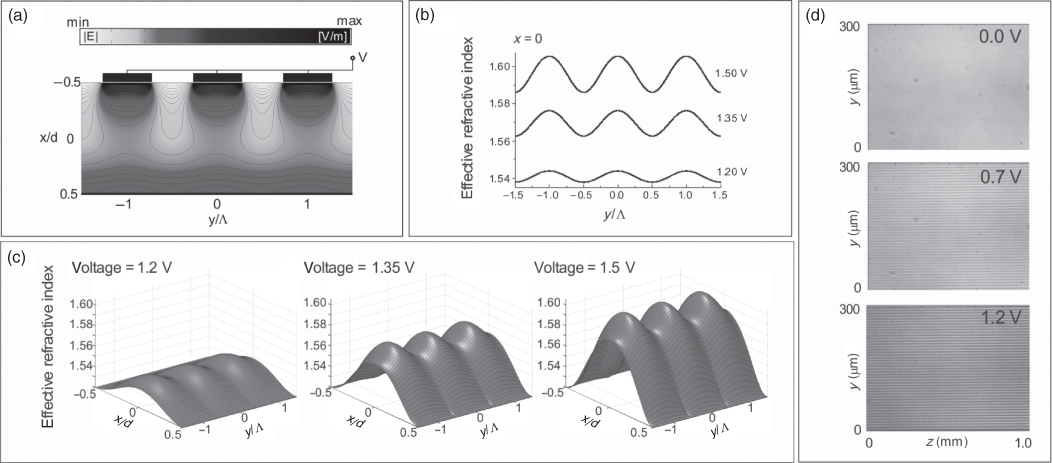
Experimentally, the formation of a periodic lattice was tested with an optical polarizing (petrographic) microscope, placing the sample between crossed polarizers. Figure 10.3d shows typical results for the sample with Λ = 8 μm and d = 6 μm: at V = 0 V, no modulation in optical properties can be observed, whereas for biases above 0.7 V, a periodic modulation is impressed, with index contrast growing with bias.
The structure tunability, including waveguiding, can be achieved in four different ways: by changing the employed NLC and therefore its optical properties (including birefringence), by varying the thickness of the NLC layer d, by modifying the electrode geometry (i.e., the width of single fingers and their mutual separation) and, finally, by reorienting the optic axis via an external bias. After manufacturing the sample, the last approach is the only viable one. For example, the strength of discrete diffraction can be adjusted by the applied bias, as shown in Figure 10.4a: by increasing the voltage, the light transfer across adjacent channels diminishes because of higher and higher barriers separating the waveguides. In other words, light confinement gets stronger within each channel, causing a longer coupling length. However, saturation of reorientation tends to flatten the transverse index distribution when an excessive voltage is applied, weakening the spatial definition of each guiding channel. We stress that, in the design of 1D waveguide arrays in NLC, a fundamental role is played by the degree of nonlocality, directly linked to d (Chapter 11) [68]. In fact, the intermolecular interactions are responsible for the diffusion of the induced orientation even in regions not under the electrodes (i.e., where the external electric field is negligible), smoothening the index distribution, and reducing the confinement; hence, in order to obtain narrow guides, it is necessary to employ a small thickness d. Figure 10.4b shows discrete diffraction versus layer thickness d for a fixed electrode pattern and bias.
Figure 10.4 Coupling strength (at λ = 1064 nm) dependence on geometry and applied voltage. (a,b) Numerical simulations for a Gaussian beam with 2 μm initial waist propagating in the NLC array with 6 μm period (darker coloring corresponds to higher light intensity). Discrete diffraction for d = 5 μm (a) versus applied voltage in z = 1 mm and (b) versus cell thickness for V = 1.2 V. (c) Coupling distance versus bias for various geometric parameters of the array (at least one of the parameters is indicated next to each line. Dashed lines are used for Λ = 5 μm; and solid lines, for d = 5 μm). (d) Coupling distance versus NLC thickness for an electrode periodicity of 6 μm and an applied voltage V = 1.2 V.
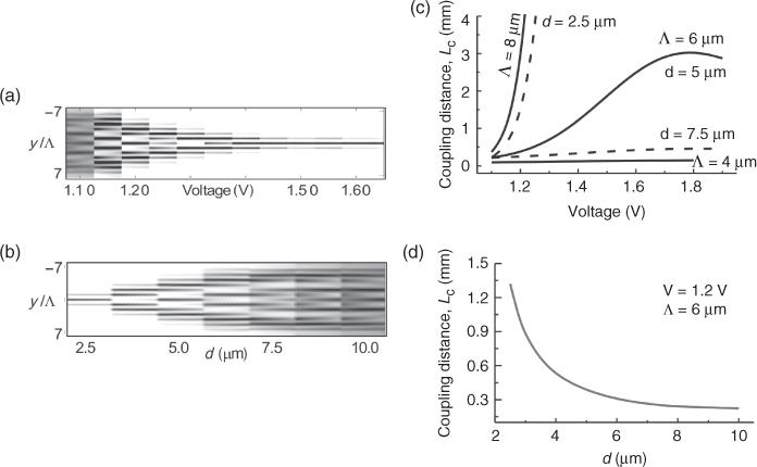
As discrete diffraction relies on the coupling between neighboring channels, the optical properties of the array can be described by the coupling distance LC, defined as the propagation distance after which the energy is transferred from one channel to the adjacent ones [69]. At any given wavelength, variations of the coupling distance can be computed with a two-dimensional mode solver. Figure 10.4c,d shows typical tuning curves: similar to one-dimensional coupled slab waveguides, the coupling distance depends exponentially on the refractive index contrast (here related to bias) and the spacing between waveguides. By reducing the NLC thickness, it is possible to better define the channel waveguides, resulting in increased coupling distances (Figure 10.4c,d). As expected, the latter can also be achieved by increasing the electrode periodicity (Fig. 10.4c). In actual devices, tunability is achieved by acting on the external voltage, as shown in Figure 10.4a,c. As previously discussed, for a fixed cell thickness, the coupling distance initially increases with voltage, until saturation becomes relevant and eventually produces a net decrease of coupling length.
Detailed numerical analyses have proved that an optimum ratio between electrode width and NLC thickness needs to be satisfied in order to maximize tunability in the range of applied biases. In actual experiments, several coupling distances have to be available because the observation window is significantly limited by scattering losses.
10.4 Discrete Diffraction and Discrete Solitons
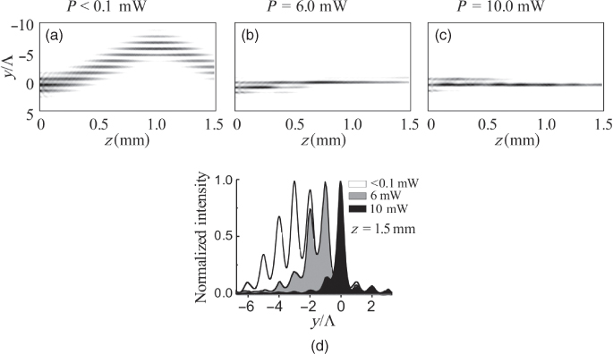
Experiments were performed in 5- to 6- μm-thick NLC cells with comb periodicity of 6 μm. A beam from a Nd:YAG laser (λ = 1064 nm) was focused with a microscope objective to a spot of approximately 4 μm (in diameter) at the entrance of the sample. The beam propagation in the NLC layer was recorded by a high-resolution CCD camera imaging the photons scattered from the top of the sample in the x-direction. Figure 10.5a,b shows experimental results on light propagation for various input beam powers. At zero bias no light confinement occurs across y: the input beam diffracts in the transverse yz-plane (as in a homogeneous medium) (Fig. 10.5a); the beam diverges and progressively reduces its intensity, becoming hardly visible after a few Rayleigh ranges. Conversely, when the cell is biased, a periodic photonic lattice is formed and discrete diffraction takes place, with features depending on the applied voltage. Figure 10.5b shows discrete propagation of an input beam launched into a single channel for a voltage V = 1.1 V (sufficient to create an array of well-defined waveguides); owing to discrete diffraction, the energy is redistributed among the channels, as visible in Figure 10.5c graphing the transverse profiles of the beam in z = 1.4 mm (gray profiles are numerical simulations shown for comparison). In z = 1.4 mm, the excitation of power P = 2 mW in a single input waveguide is redistributed in 13 adjacent channels. It is to be noted that the divergence in this case is significantly lower than in the case of standard (continuous) diffraction in a uniform planar waveguide (i.e., no applied voltage), indicated by dashed lines. Figure 10.5b presents the nonlinear changes in discrete propagation for various input powers, with the corresponding transverse intensity profiles at z = 1.4 mm plotted in Figure 10.5c.
Figure 10.5 (a) Linear propagation (standard diffraction) in the homogeneous planar waveguide (zero voltage). (b) Discrete propagation (V = 1.1 V) for various input powers and a beam launched into a single channel. A discrete soliton forms at 10 mW. (c) Measured transverse intensity profiles (black lines) at z = 1.4 mm, corresponding to the cases in (b). The calculated profiles matching the experimental conditions are represented in gray. (d) Assembled photosequence versus applied voltage showing the diffraction of a 6 mW Nd:YAG beam in z = 1 mm.
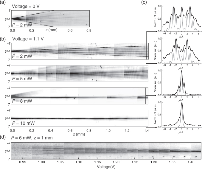
As anticipated, at high powers, the effective index of the input waveguide(s) is raised by light itself through reorientation. Such increase can counteract discrete diffraction via an induced phase mismatch between the excited waveguide(s) and the unexcited portion of the periodic structure. For sufficiently high intensities, the nonlinear response can overcome diffraction and support spatial self-localization, that is, self-confined light propagation in a channel subset of the array. The resulting discrete beam, with a transverse profile invariant along propagation, is called discrete spatial soliton [1–3]: discrete solitons may exist in the form of partially delocalized or “wide” soliton with energy distributed among several channels, or in the form of localized or “narrow” solitons with all the energy confined in the input waveguide, as in the last panel of Figure 10.5b. Owing to the specific mechanism for light self-confinement in discrete systems, the power requirements for solitons are lower than in slab waveguides or bulk media. Specifically, discrete solitons in NLC result from the interplay between evanescent coupling, nonlinear response, and nonlocality (owing to intermolecular elastic forces). In this scenario, the giant nonlinear response, typical of molecular reorientation in NLC, allows observing discrete spatial solitons at a few milliWatts.
Besides self-effects controlled by light power, confinement can also be adjusted by bias. Figure 10.5d displays a sequence of photographs taken for an input power of 6 mW after a propagation length of 1 mm, showing transverse coupling and discrete propagation versus applied voltage: higher biases result in reduced angular beam divergence, with the coupling distance becoming longer. At low voltages, the beam energy distributes among several channels, whereas for voltages above 1.45 V, it is confined in a single waveguide.
10.5 Optical Multiband Vector Breathers
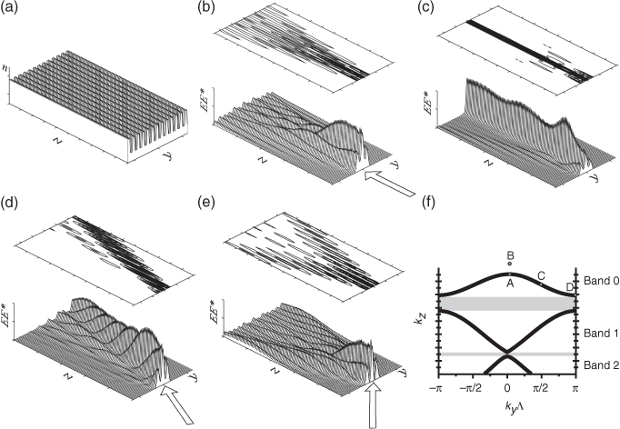
A multiband discrete breather originates from the superposition of (two or more) Floquet–Bloch (FB) modes of the lattice belonging to different bands of the dispersion diagram [59, 70]. Such modes are characterized by slightly different propagation constants. Analogous to vector solitons [71–74], discrete breathers stem from individual modes coupled via cross-phase modulation. The resulting two-component beam is capable of overcoming diffraction, even when constituent modes from each band (or gap) either diffract linearly or are localized into a discrete soliton [23]. In the case presented here, none of the individual modes is able to self-trap. The propagation constants of each mode as well as the breathing period can be effectively adjusted by tuning the array dispersion via the electro-optic reorientational response of NLC. With reference to the NLC array previously illustrated, it is possible to numerically compute the dispersion diagram of the linear eigenmodes versus applied bias by solving the differential equations governing molecular reorientation and then calculating the effective index for TM modes. To this extent, the well-known FB analysis can be used [59]. Figure 10.6a displays the dispersion diagram calculated for the NLC array with d = Λ = 6 μm and an applied voltage V = 0.9 V: multiple (linear) FB bands (each corresponding to different FB modes) are separated by gaps (in gray), similar to solid-state physics. The full model based on FB theory yields discrete solitons belonging to the semi-infinite gap 0, as well as spatial gap solitons [75, 76] or FB solitons [23] involving two or more gaps. Figure 10.6d,e shows the intensity distribution of modes belonging to bands 0 and 1 for a transverse wave vector ky = π/Λ. As in NLC arrays the effective index is easily modulated by the external bias (Fig. 10.6b), widths and location of the individual bands, and therefore the corresponding gaps, can be experimentally controlled and adjusted. Once again, the system is a tunable one-dimensional photonic lattice. Figure 10.6c shows the variations in the size of gap 1 versus bias. For voltages below 1.3 V, the effective index increases with bias and the gap widens; when the voltage exceeds 1.3 V, the nonlocal and saturating character of the reorientational response reduces the index modulation (Fig. 10.6b), with a reduction in gap width. A proper input superposition of FB linear modes can lead to light localization via cross-phase modulation, yielding periodic oscillations of the intensity distribution along propagation, that is, a multiband optical breather [51]. Figure 10.6f,h shows numerical simulations of the superposition of modes (which cannot self-trap when launched individually) from the two upper bands. FB modes belonging to band 0 (with intensity maxima in the channel regions) can be excited by a wide Gaussian beam launched between two channels (Fig. 10.6f). Conversely, modes of band 1 possess intensity maxima in between channels and can be excited by a narrow Gaussian beam centered between two waveguides (Fig. 10.6g). A symmetric breather, with spatially localized and periodically oscillating propagation (Fig. 10.6h) can be obtained when two Gaussian beams are injected together, combining their powers and interacting via cross-phase modulation.
Figure 10.6 (a) Calculated bandgap diagram (i.e., dispersion relation) for an NLC waveguide array with Λ = d = 6 μm and for V = 0.9 V. (b) Effective index modulation at x = 0 (lines), as well as two-dimensional distribution (contour plot) at various voltages. (c) Calculated width of gap 1 versus bias. (d,e) Two-dimensional modal profiles (darker areas correspond to higher light intensity) for bands 0 and 1 and normalized Bloch wave vector kyΛ/π = 1; the contour lines correspond to the refractive index distribution shown in Figure 10.3b. (f,g) Low power light propagation in the NLC array (for V = 1 V) computed with the beam propagation method (BPM) for a 0.2 mW Gaussian beam either (f) wide or (g) narrow injected between two adjacent waveguides. Modes belonging to (f) band 0 and (g) band 1 are excited, giving rise (h) to a vector-symmetric breather when superimposed.
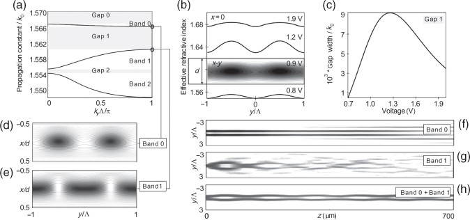
In order to experimentally generate a symmetric breather, we used a narrow 1064-nm Gaussian beam (with a waist of about 5 μm) from a Nd:YAG laser. It was launched in the region between two neighboring channels to ensure the excitation of FB modes belonging to the first two bands. In such a configuration, a larger spatial overlap is obtained for the modes belonging to band 1 because of the chosen input profile. In fact, at low powers (P = 0.2 mW in Figure 10.7a) the diffraction pattern resembles the one in Figure 10.6g. As the power increases, light confinement can be enhanced via light-induced reorientation, thus making the excitation more effective toward modes from band 0 with respect to those from band 1. At high enough excitations (i.e., when the modes carry equal powers of 7 mW) a symmetric breather is obtained, with several oscillations clearly visible in Figure 10.7b; the on-axis light intensity (i.e., for y = 0) is displayed in Figure 10.7c. Linear propagation losses, mostly due to elastic Rayleigh scattering, are also apparent in the latter graph.
Figure 10.7 Experimental results on vector breathers in an NLC array with Λ = 6 μm and bias V = 1 V. (a) Low (P = 0.2 mW) and (b) high (P = 7 mW) power propagation of a Gaussian beam launched with waist 5 μm (along y) in between two channels. (c) On-axis light intensity distributions along propagation, corresponding to the cases in (a) and (b). (d) Photosequence showing the breather evolution for various applied voltages. (e) Measured variation in breathing period versus bias.
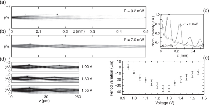
The breathing period dependence versus voltage was also measured, as in the sequence of photographs in Figure 10.7d. As the width of gap 1 can be effectively changed by bias (consistent with the variation of the effective index) as shown in Figure 10.6c, the oscillation period reaches its minimum for a voltage of about 1.3 V, corresponding to the minimum width of gap 1. Above this value, the bandgap width reduces again, resulting in a longer period; such a trend is confirmed by experiments, as shown in Figure 10.7e.
10.6 Nonlinear Angular Steering
Discrete systems can be employed for nonlinear beam steering because they lack rotational symmetry. At variance with continuous (isotropic) systems where all directions are equivalent, discrete arrays do not support solitary waves propagating aslant across the lattice. Whereas light beams can obliquely travel across a photonic array in the linear regime (with special directions defined by the minimum diffraction angle), discrete solitons can only propagate straight with zero transverse velocity: a discrete soliton travels along a waveguide channel nonlinearly detuned from the rest of the array.
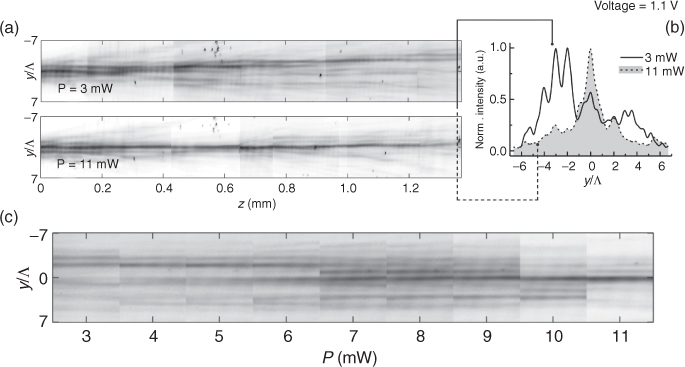
Figure 10.8 demonstrates nonlinear beam steering in the NLC array with Λ = 6 μm, d = 5 − 6 μm and V = 1.1 V, launching a Gaussian beam of waist wy = 10 μm at an angle of ![]() with respect to z. At an input power of 3 mW, the tilted beam undergoes discrete diffraction; for P = 11 mW, light localizes in the input channel (Fig. 10.8a). The intensity cross sections in z = 1.4 mm illustrate an all-optically induced lateral shift of the beam (Fig. 10.8b). Nonlinear steering is also clearly visible in Figure 10.8c, displaying the output (i.e., for z = 1.4 mm) intensity distribution for various excitations in the range 3–11 mW. Such phenomenon has potential applications in all-optical switching, steering, and multiport routing [50, 77].
with respect to z. At an input power of 3 mW, the tilted beam undergoes discrete diffraction; for P = 11 mW, light localizes in the input channel (Fig. 10.8a). The intensity cross sections in z = 1.4 mm illustrate an all-optically induced lateral shift of the beam (Fig. 10.8b). Nonlinear steering is also clearly visible in Figure 10.8c, displaying the output (i.e., for z = 1.4 mm) intensity distribution for various excitations in the range 3–11 mW. Such phenomenon has potential applications in all-optical switching, steering, and multiport routing [50, 77].
Figure 10.8 Experimental demonstration of nonlinear beam steering. (a) Minimum discrete diffraction of a 3 mW beam tilted by ![]() and discrete soliton propagating straight for a power P = 11 mW. (b) Corresponding intensity profiles along y at z = 1.4 mm. (c) Assembled photosequence of discrete light propagation (at z = 1.4 mm) versus input power.
and discrete soliton propagating straight for a power P = 11 mW. (b) Corresponding intensity profiles along y at z = 1.4 mm. (c) Assembled photosequence of discrete light propagation (at z = 1.4 mm) versus input power.
10.7 Landau–Zener Tunneling
LZ tunneling is another important topic related to optically discrete systems. LZ tunneling was introduced in the context of two-level quantum systems where the interaction (transition) between two different energy eigenstates can take place [78]; it may be generally associated with any quantized system accelerated by an external force [59]. In the nonadiabatic limit, the external perturbation makes the transition between different energy levels possible with a finite probability. In the case of optical lattices, light can tunnel between different FB bands when a refractive index gradient (acting as the perturbation that couples the eigenstates) is applied across the periodically modulated refractive index [31, 33]. In close analogy with semiconductor physics, a light beam, initially coupled to one single band, can transfer to another band if a nonadiabatic externally forced gradient is appreciable. The observable outcome is that the light intensity profile and/or the propagation direction will change due to tunneling. In the case discussed here, the gradient in refractive index responsible for the interband coupling is induced by light itself. Such all-optical acceleration in an NLC waveguide array is relatively easy. An implementation based on the thermal response (Chapter 9) is sketched in Figure 10.9a–c. An intense and wide Gaussian beam (the pump) is injected in the array, increasing the local temperature and changing in turn the refractive index; the pump beam determines a decrease in extraordinary refractive index via thermo-optic self-defocusing. In our structure (Fig. 10.2a), the thermal NLC response near the isotropic–nematic transition temperature (close to room temperature for PCB) induces a defocusing nonlinearity and made it dominant with respect to the reorientational one by employing the bias to operate at large orientation angles.
Figure 10.9 (a–c) An approach to Landau–Zener tunneling in NLC arrays. The refractive index gradient or acceleration is obtained via the thermal nonlinear response induced by the wide Gaussian beam pump. (d) Schematic drawing of the dispersion (bandgap) diagram. Black arrows, normal to the dispersion curve, indicate a maximum in propagation angle for modes of two different bands (here bands 0 and 1). The LZ transition between these two states is represented by a dashed line. (e) Numerically simulated propagation of FB modes of band 0 at the maximum transverse velocity, and (f) Landau–Zener tunneling between bands 0 and 1. In the transition region (indicated by a dashed line), energy is transferred to band 1 and the beam propagates at a larger angle than in band 0.
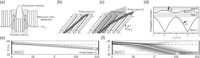
A second low-intensity beam (the probe) is launched into the perturbed photonic structure shown in Figure 10.9a, exciting FB modes able to undergo LZ tunneling to other bands. When a negative index change is produced by the pump in the transition regions (Fig. 10.9a), the probe, which is initially a superposition of FB modes of the upper band (e.g., band 0 in Figure 10.9d), is transferred to the lower band (band 1) and propagates through the lattice at an angle (with z) larger than the initial one. This is due to the larger group velocity, as indicated by the normal to the dispersion curve (black arrow in Figure 10.9d). Thus, the probe beam undergoes all-optical angular steering and spatial switching via LZ tunneling.
Mathematical modeling of the LZ phenomenon requires the solution of three coupled differential equations, including the Euler–Lagrange equation for molecular reorientation due to bias, the wave equation for linear propagation of the probe, and an equation for the pump-driven temperature variation. After some approximations, the model can be recast as a single dimensionless Schrödinger-like equation [52] and, eventually, as the original Zener model [78] predicting tunneling between bands in solid-state physics. Typical numerical simulations are shown in Figure 10.9e,f.
One approach for experimentally verifying LZ tunneling in a lattice consists in measuring the shifts of the intensity profile maxima of the excited FB modes, as they are not the same from band to band [31]. Unfortunately, such an approach cannot be adopted when the lattice period and wavelength are comparable, as it is in the case of micrometric lattices illuminated by near-IR light. Alternatively, as each FB mode in a given band has a maximum propagation angle, LZ tunneling can be detected by observing the change in the probe propagation direction due to the pump-induced acceleration. The higher the band number, the higher the maximum propagation angle (Fig. 10.9d), as shown in Figure 10.9e,f.
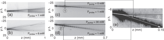
The demonstration of LZ tunneling was performed by using a 1D NLC lattice with Λ = 4 μm and d = 6 μm. A probe at λ = 1064 nm and power up to 6 mW was used to test the self-defocusing nonlinear response, obtaining a more diffracting beam in yz (Fig. 10.10a,b). Then two mutually incoherent beams from a Nd:YAG laser at λ = 1064 nm were employed to act as pump and probe. An intense Gaussian pump of waist wy = 15 μm (about four array periods and a corresponding Rayleigh distance of about 1 mm) generated the two transition regions with acceleration, ensuring no overlap with the probe after tunneling. The probe (with waist wy = 1.5Λ = 6 μm and power 1 mW) was initially coupled to band 0 at its maximum transverse velocity (for zero pump), discretely diffracting. A pump power above 25 mW was sufficient for all-optical acceleration and band coupling; for instance, at 30 mW (Fig. 10.10d), the probe tunneled from first to second band, propagating at a larger angle in the yz-plane (Fig. 10.10d,e). The direction of the pump in Figure 10.10c–e is indicated by the black dashed line.
Figure 10.10 Experimental results in a cell with Λ = 4 μm and d = 6 μm, biased at 1.9 V. (a) Linear discrete diffraction and (b) self-defocusing of a beam in the array. Increasing the power also increases the beam spreading. (c–e) Landau–Zener tunneling of a 1mW-probe observed when a 30 mW pump was launched along z. (c) The probe, initially in band 0, is injected at the maximum transverse velocity. (d) After tunneling, the probe transfers to band 1 and propagates at a different angle. (e) The zooming-in of cases (c) and (d) underlines the increase in propagation angle after LZ tunneling.
10.8 Bloch Oscillations
BO were originally discussed for electrons in a periodic potential with an applied electric field [79]. In optics, BO can be obtained in waveguide arrays when a linear gradient is added to the transverse periodicity of the refractive index modulation [26–29]. As an effect of such index distribution, a light beam oscillates periodically in the transverse direction during propagation, retrieving initial position and profile after each full cycle. Linear and nonlinear optical BO were experimentally observed in AlGaAs waveguides [27], polymer arrays [28], and arrays of curved waveguides [64]. Similar effects are accessible in NLC arrays, as well. In order to introduce a linear refractive index gradient, one can apply a voltage linearly varying across the comb-shaped electrode or alter the stripe spacing/width (Fig. 10.11a,b). The simplest approach is to employ an NLC layer with thickness linearly changing with y [i.e., d = d(y)], as in Figure 10.11c.
Figure 10.11 (a–c) Configurations for observing BO in NLC waveguide arrays. The third option (c) appears the simplest in terms of fabrication.
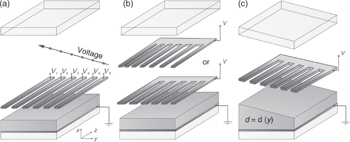
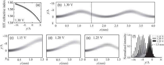
Figure 10.12a shows the linear index distribution obtained in the NLC midlayer for a thickness varying with a slope of ![]() (thickness change of 1.64 μm for each 100 μm along y) and d(y = 0) = 3.672 μm, electrode period of 4 μm, and three applied voltages. Owing to the geometry of the guiding layer, a quasilinear gradient is added to the periodic modulation, resulting in slight differences in the parameters of neighboring channels.
(thickness change of 1.64 μm for each 100 μm along y) and d(y = 0) = 3.672 μm, electrode period of 4 μm, and three applied voltages. Owing to the geometry of the guiding layer, a quasilinear gradient is added to the periodic modulation, resulting in slight differences in the parameters of neighboring channels.
Amplitude and period of the BO can be changed by acting on the array geometry or the bias, thus modifying the effective index distribution. The variation of BO period with voltage is shown in Figure 10.12b–e for a TM-polarized Gaussian beam of waist 10 μm (i.e., a broad beam) launched along z. The injected beam moves toward the outermost waveguide (i.e., the channel where the index is higher) until it is Bragg-reflected at the edge of the first Brillouin zone in transformed space; after reflection, the beam moves back toward the innermost guide, undergoing another Bragg reflection. The beam oscillates periodically in the transverse space, with the initial profile reproduced after a complete BO (Fig. 10.12b). Routing can be achieved by acting on the applied voltage to control the output beam position (at z = 1.5 mm in Figure 10.12f).
Figure 10.12 (a) Refractive index distribution in the middle of an NLC layer with varying thickness for 1.3 V. The periodicity of the ITO electrode is 4 μm and the thickness slope α = 56′, with α being the angle between the top glass surface and y-direction. (b–e) BPM simulations of low power BO for a Gaussian beam with input waist of 10 μm and various voltages. In all cases, the input power is low enough to leave the index distribution unaltered by light. (f) The intensity profiles calculated in z = 1.5 mm illustrate the bias-controlled change in beam position.
Finally, changes in beam propagation direction can also be induced all-optically, similar to the previously demonstrated nonlinear steering. Figure 10.13a–c shows the calculated discrete propagation of a beam undergoing BO in the linear and nonlinear regime. Figure 10.13d shows the corresponding output intensity profiles (in z = 1.5 mm). As nonlinear effects become appreciable, the induced detuning alters the phase matching required for BO, until the input beam remains confined in the launch channel(s).
Figure 10.13 (a–c) Change of beam propagation with power. A Bloch oscillating beam as in (a) can be trapped in the input channel at high enough power as in (c). (d) Output (at z = 1.5 mm) intensity distributions corresponding to the previous cases (a–c).
10.9 Conclusions
Spatial optical solitons in NLCs have their discrete counterpart in NLC waveguide arrays. One-dimensional arrays can be easily implemented and tuned taking advantage of the NLC electro-optic response, giving rise to a wealth of all-optical discrete phenomena at relatively low powers, from tunable diffraction to self-confinement, angular steering and switching, LZ tunneling, power-controlled BO, and vector breathers. The variety of effects and versatility of the material platform make discrete optical phenomena in NLCs and discrete nematicons an excellent approach toward all-optical signal readdressing and light reconfigurable circuits.
Acknowledgments
We are particularly grateful to Andrea Fratalocchi for his essential contributions to the work reported here.
1. F. Lederer, S. Darmanyan, and A. Kobyakov. Discrete solitons, in Spatial Solitons, ed. S. Trillo and W. Torruellas. Wiley, New York, 2002.
2. F. Lederer, G. I. Stegeman, D. N. Christodoulides, G. Assanto, M. Segev, and Y. Silberberg. Discrete solitons in optics. Phys. Rep., 463:1–126, 2008.
3. A. A. Sukhorukov, Y. S. Kivshar, H. S. Eisenberg, and Y. Silberberg. Spatial optical solitons in waveguide arrays. IEEE J. Quantum Electron., 39:31–50, 2003.
4. R. Morandotti, H. S. Eisenberg, Y. Silberberg, M. Soler, and J. S. Aitchison. Self-focusing and defocusing in waveguide arrays. Phys. Rev. Lett., 86:3296–3299, 2001.
5. H. S. Eisenberg, Y. Silberberg, R. Morandotti, A. R. Boyd, and J. S. Aitchison. Diffraction management. Phys. Rev. Lett., 85:1863–1866, 2000.
6. P. Millar, J. S. Aitchison, J. U. Kang, G. I. Stegeman, A. Villeneuve, G. T. Kennedy, and W. Sibbett. Nonlinear waveguide arrays in AlGaAs. J. Opt. Soc. Am. B, 14:3224–3231, 1997.
7. D. Cheskis, S. Bar-Ad, R. Morandotti, J. S. Aitchison, H. S. Eisenberg, Y. Silberberg, and D. Ross. Strong spatiotemporal localization in a silica nonlinear waveguide array. Phys. Rev. Lett., 91:223901, 2003.
8. T. Pertsch, U. Peschel, F. Lederer, J. Burghoff, M. Will, S. Nolte, and A. Tunnermann. Discrete diffraction in two-dimensional arrays of coupled waveguides in silica. Opt. Lett., 29:468–470, 2004.
9. T. Pertsch, T. Zentgraf, U. Peschel, A. Brauer, and F. Lederer. Anomalous refraction and diffraction in discrete optical systems. Phys. Rev. Lett., 88:093901, 2002.
10. N. K. Efremidis, S. Sears, D. N. Christodoulides, J. W. Fleischer, and M. Segev. Discrete solitons in photorefractive optically induced photonic lattices. Phys. Rev. E, 66:046602, 2002.
11. D. N. Christodoulides, F. Lederer, and Y. Silberberg. Discretizing light behaviour in linear and nonlinear waveguide lattices. Nature, 424:817–823, 2003.
12. R. Iwanow, R. Schiek, G. I. Stegeman, T. Pertsch, F. Lederer, Y. Min, and W. Sohler. Observation of discrete quadratic solitons. Phys. Rev. Lett., 93:113902, 2004.
13. D. N. Christodulides and E. D. Eugenieva. Blocking and routing discrete solitons in two-dimensional networks of nonlinear waveguide arrays. Phys. Rev. Lett., 87:233901, 2001.
14. R. Morandotti, U. Peschel, J. S. Aitchison, H. S. Eisenberg, and Y. Silberberg. Dynamics of discrete solitons in optical waveguide arrays. Phys. Rev. Lett., 83:2726–2729, 1999.
15. W. Królikowski and Y. S. Kivshar. Soliton-based optical switching in waveguide arrays. J. Opt. Soc. Am. B, 13:876–887, 1996.
16. O. Bang and P. Miller. Exploiting discreteness for switching in waveguide arrays. Opt. Lett., 21:1105–1107, 1996.
17. D. N. Christodoulides and R. I. Joseph. Discrete self focusing in nonlinear arrays of coupled waveguides. Opt. Lett., 13:794–796, 1988.
18. C. Etrich, F. Lederer, B. Malomed, T. Peschel, and U. Peschel. Optical solitons in media with a quadratic nonlinearity, in Progress in Optics. Vol. 41. ed. E. Wolf, Elsevier Science Publishers, Amsterdam, pp. 483–568, 2000.
19. J. Meier, G. I. Stegeman, Y. Silberberg, R. Morandotti, and J. S. Aitchison. Nonlinear optical beam interactions in waveguide arrays. Phys. Rev. Lett., 93:093903, 2004.
20. J. Fleischer, G. Bartal, O. Cohen, T. Schwartz, O. Manela, B. Freedman, M. Segev, H. Buljan, and N. Efremidis. Spatial photonics in nonlinear waveguide arrays. Opt. Express, 13:1780–1796, 2005.
21. J. W. Fleisher, M. Segev, N. K. Efremidis, and D. N. Christodoulides. Observation of two-dimensional discrete solitons in optically induced nonlinear photonic lattices. Nature, 422:147–150, 2003.
22. A. A. Sukhorukov and Y. S. Kivshar. Generation and stability of discrete gap solitons. Opt. Lett., 28:2345–2347, 2003.
23. D. Mandelik, H. S. Eisenberg, Y. Silberberg, R. Morandotti, and J. S. Aitchison. Observation of mutually trapped multiband optical breathers in waveguide array. Phys. Rev. Lett., 90:253902, 2003.
24. D. Mandelik, H. S. Eisenberg, Y. Silberberg, R. Morandotti, and J. S. Aitchison. Band-gap structure of waveguide arrays and excitation of Floquet-Bloch solitons. Phys. Rev. Lett., 90:053902, 2003.
25. O. Cohen, T. Schwartz, J. W. Fleischer, M. Segev, and D. N. Christodoulides. Multiband vector lattice solitons. Phys. Rev. Lett., 91:113901, 2003.
26. U. Peschel, T. Pertsch, and F. Lederer. Optical Bloch oscillations in waveguide arrays. Opt. Lett., 23:1701–1703, 1998.
27. R. Morandotti, U. Peschel, J. S. Aitchison, H. S. Eisenberg, and Y. Silberberg. Experimental observation of linear and nonlinear optical Bloch oscillations. Phys. Rev. Lett., 83:4756–4759, 1999.
28. T. Pertsch, P. Dannberg, W. Elflein, A. Bräuer, and F. Lederer. Optical Bloch oscillations in temperature tuned waveguide arrays. Phys. Rev. Lett., 83:4752–4755, 1999.
29. G. Lenz, R. Parker, M. C. Wanke, and C. M. de Sterke. Dynamical localization and AC Bloch oscillations in periodic optical waveguide arrays. Opt. Comm., 218:87–92, 2003.
30. H. Trompeter, W. Krolikowski, D. N. Neshev, A. S. Desyatnikov, A. A. Sukhorukov, Y. S. Kivshar, T. Pertsch, U. Peschel, and F. Lederer. Optical Bloch oscillations and Zener tunneling in two-dimensional photonic lattices. Topical Meeting on Nonlinear Guided Waves and their Applications, ThD1, OSA, Dresden, Germany, 2005.
31. R. Khomeriki and S. Ruffo. Nonadiabatic Landau-Zener tunneling in waveguide arrays with a step in the refractive index. Phys. Rev. Lett., 94:113904, 2005.
32. B. Wu and Q. Niu. Nonlinear Landau-Zener tunneling. Phys. Rev. A, 61:023402, 2000.
33. V. V. Konotop, P. G. Kevrekidis, and M. Salerno. Landau-Zener tunneling of Bose-Einstein condensates in an optical lattice. Phys. Rev. A, 72:023611, 2005.
34. T. Pertsch, U. Peschel, and F. Lederer. All-optical switching in quadratically nonlinear waveguide arrays. Opt. Lett., 28:102–104, 2003.
35. R. A. Vicencio, M. I. Molina, and Y. S. Kivshar. Switching of disrete optical solitons in engineered waveguide arrays. Phys. Rev. E, 90:026602, 2004.
36. Y. V. Kartashov, L. C. Crasovan, A. S. Zelenina, V. A. Vysloukh, A. Sanpera, M. Lewenstein, and L. Torner. Soliton eigenvalue control in optical lattices. Phys. Rev. Lett., 93:143902, 2004.
37. M. Peccianti, G. Assanto, A. De Luca, C. Umeton, and I. C. Khoo. Electrically assisted self-confinement and waveguiding in Planar Nematic Liquid Crystal cells. Appl. Phys. Lett., 77:7–9, 2000.
38. G. Assanto and M. Peccianti. Spatial solitons in nematic liquid crystals. IEEE J. Quantum Electron., 39:13–21, 2003.
39. G. Assanto, M. Peccianti, and C. Conti. Nematicons: Optical spatial solitons in nematic liquid crystals. Opt. Photon. News, 14:44–48, 2003.
40. G. Assanto and M. A. Karpierz. Nematicons: Self-localized beams in nematic liquid crystals. Liq. Cryst., 36:1161–1172, 2009.
41. M. Peccianti, C. Conti, G. Assanto, A. De Luca, and C. Umeton. Routing of highly anisotropic spatial solitons and modulational instability in liquid crystals. Nature, 432:733–737, 2004.
42. G. Assanto, M. Peccianti, and A. Fratalocchi. Spatial solitons in nematic liquid crystals: From bulk to discrete. Opt. Express, 15:5248–5259, 2007.
43. A. Fratalocchi, G. Assanto, K. A. Brzdakiewicz, and M. A. Karpierz. Discrete propagation and spatial solitons in nematic liquid crystals. Opt. Lett., 29:1530–1532, 2004.
44. A. Fratalocchi, G. Assanto, K. A. Brzdakiewicz, and M. A. Karpierz. Discrete light propagation and self-trapping in liquid crystals. Opt. Express, 13:1808–1815, 2005.
45. A. Fratalocchi and G. Assanto. Discrete light localization in one-dimensional nonlinear lattices with arbitrary nonlocality. Phys. Rev. E, 72:066608, 2005.
46. K. A. Brzdakiewicz, M. A. Karpierz, A. Fratalocchi, and G. Assanto. Nematic liquid crystal waveguide arrays. Opto-Electron. Rev., 13:107–112, 2005.
47. K. A. Brzdakiewicz, M. A. Karpierz, A. Fratalocchi, and G. Assanto. Discrete light propagation and self-localization in voltage-controlled arrays of channel waveguides in undoped nematic liquid crystals. Mol. Cryst. Liq. Cryst., 453:191–202, 2006.
48. A. Fratalocchi and G. Assanto. Governing soliton splitting in one-dimensional lattices. Phys. Rev. E, 73:046603, 2006.
49. A. Fratalocchi, G. Assanto, and M. A. Karpierz. Discrete optics in liquid crystalline lattices. IEEE LEOS Newsletter, 2:11–16, 2006.
50. A. Fratalocchi, G. Assanto, K. A. Brzdakiewicz, and M. A. Karpierz. All-optical switching and beam steering in tunable waveguide arrays. Appl. Phys. Lett., 86:051112, 2005.
51. A. Fratalocchi, G. Assanto, K. A. Brzdakiewicz, and M. A. Karpierz. Optical multiband vector breathers in tuneable waveguide arrays. Opt. Lett., 30:174–176, 2005.
52. A. Fratalocchi and G. Assanto. All-optical Landau-Zener tunneling in waveguide arrays. Opt. Express, 14:2021–2026, 2006.
53. A. Fratalocchi, G. Assanto, K. A. Brzdakiewicz, and M. A. Karpierz. Optically-induced Zener tunneling in one dimensional lattices. Opt. Lett., 31:790–792, 2006.
54. A. Fratalocchi, K. A. Rutkowska, M. A. Karpierz, and G. Assanto. Light induced angular steering via Floquet-Bloch band-tunnelling in one-dimensional liquid crystalline photonic lattices. Opto-Electron. Rev., 15:210–214, 2007.
55. K. A. Brzdakiewicz, M. A. Karpierz, A. Fratalocchi, and G. Assanto. Bloch oscillations in nematic liquid crystals waveguide arrays. Proc. SPIE, 5949:178, 2005.
56. S. Somekh, E. Garmire, A. Yariv, H. L. Garvin, and R. G. Hunsperger. Channel optical waveguide directional couplers. Appl. Phys. Lett., 22:46–48, 1973.
57. S. M. Jensen. The nonlinear coherent coupler. IEEE J. Quantum Electron., 18:1580–1583, 1982.
58. S. Longhi. Discrete diffraction and shape-invariant beams in optical waveguide arrays. Phys. Rev. A, 79:033847, 2009.
59. K. Sakoda. Optical Properties of Photonic Crystals. Springer, Berlin, 2001.
60. D. Mandelik, R. Morandotti, J. S. Aitchison, and Y. Silberberg. Gap solitons in waveguide arrays. Phys. Rev. Lett., 92:093904, 2004.
61. S. Flach and C. R. Willis. Discrete breathers. Phys. Rep., 295:181–264, 1998.
62. A. A. Sukhorukov and Y. S. Kivshar. Multigap discrete vector solitons. Phys. Rev. Lett., 91:113902, 2003.
63. A. S. Desyatnikov, E. A. Ostrovskaya, Y. S. Kivshar, and C. Denz. Composite band-gap Solitons in nonlinear optically induced lattices. Phys. Rev. Lett., 91:153902, 2003.
64. G. Lenz, I. Talanina, and C. M. de Sterke. Bloch oscillations in an array of curved optical waveguides. Phys. Rev. Lett., 83:963–967, 1999.
65. P. G. de Gennes and J. Prost. The Physics of Liquid Crystals, 2nd edn, Oxford University Press, London, 1993.
66. I. C. Khoo. Liquid Crystals: Physical Properties and Nonlinear Optical Phenomena. Wiley, New York, 1995.
67. D. A. Dumm, A. Fukuda, and G. R. Luckhurst. Physical Properties of Liquid Crystals: Nematics. Inspec, London, 2001.
68. A. Alberucci, A. Piccardi, M. Peccianti, M. Kaczmarek, and G. Assanto. Propagation of spatial optical solitons in a dielectric with adjustable nonlinearity. Phys. Rev. A, 82(2):023806, 2010.
69. A. Yariv. Optical Electronics in Modern Communications. Oxford Press, New York, 1997.
70. N. W. Ashcroft and N. D. Mermin. Solid State Physics. Saunders College Publishing, New York, 1976.
71. M. Mitchell, M. Segev, and D. N. Christodoulides. Observation of multihump multimode solitons. Phys. Rev. Lett., 80:4657–4660, 1998.
72. S. Darmanyan, A. Kobyakov, E. Schmidt, and F. Lederer. Strongly localized vectorial modes in nonlinear waveguide arrays. Phys. Rev. E, 57:3520–3530, 1998.
73. J. Hudock, P. G. Kevrekidis, B. A. Malomed, and D. N. Christodoulides. Discrete vector solitons in two-dimensional nonlinear waveguide arrays: Solutions, stability, and dynamics. Phys. Rev. E, 67:056618, 2003.
74. J. Meier, J. Hudock, D. N. Christodoulides, G. Stegeman, Y. Silberberg, R. Morandotti, and J. S. Aitchison. Discrete vector solitons in Kerr Nonlinear waveguide arrays. Phys. Rev. Lett., 91:143907, 2003.
75. J. W. Fleisher, T. Carmon, M. Segev, N. K. Efremidis, and D. N. Christodoulides. Observation of discrete solitons in optically induced real time waveguide arrays. Phys. Rev. Lett., 90:023902, 2003.
76. J. Feng. Alternative scheme for studying gap solitons in an infinite periodic Kerr medium. Opt. Lett., 18:1302–1304, 1993.
77. A. B. Aceves, C. De Angelis, T. Peschel, R. Muschall, F. Lederer, S. Trillo, and S. Wabnitz. Discrete self-trapping, soliton interactions, and beam steering in nonlinear waveguide arrays. Phys. Rev. E, 53:1172–1189, 1996.
78. C. Zener. Non-adiabatic crossing of energy levels. Proc. R. Soc. London, Ser. A, 137:696–702, 1932.
79. F. Bloch. Uber die quantenmechanik der elektronen in kristallgittern. Z. Physik, 52:555–600, 1928.