
15
Some FEM Topics
15.1 Symmetries
One of the principal reasons for the popularity of the FEM is the ease with which boundary conditions are handled. All of the FEM examples presented thus far have utilized boundary conditions formed by setting boundary nodes to an assigned voltage. Since we have dealt exclusively with triangular shapes with simple linear shape functions, this means that the lines connecting these nodes (an edge of the triangle) are set to a linear interpolation between these two node voltages.
A second type of boundary condition occurs when the node voltages are not assigned but the electric flux along line edges is assigned. The electric flux at a region boundary is defined as the integral of the normal component of the electric field lines crossing that boundary (in this case the triangle’s edge).
There are elegant derivations of how to translate these boundary conditions into FEM equations.1 These derivations, in turn, require some background in variational calculus and vector calculus. We will consider only a subset of the general problem, so a simpler explanation of how to set up our equations will suffice.
A symmetry boundary, or a magnetic wall, is a boundary which has zero electric flux across it. That is, the electric field at the boundary is parallel to the boundary wall (and the normal field across the boundary wall is zero).
Figure 15.1 shows an example of a symmetric structure. It may also be regarded as a subset of a larger symmetric structure.
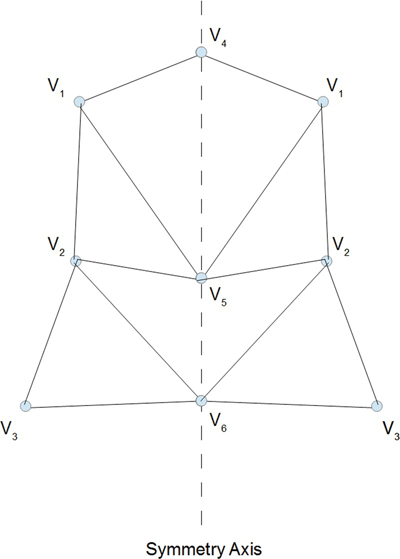
FIGURE 15.1 Example of a simple symmetric structure.
In this figure, the structure is symmetric about the labeled symmetry axis (the dashed line). Although it is not necessary for the zoning (node and triangle locations) to be symmetric about a symmetry axis, it is always possible to create them this way — if this were not possible, the structure cannot be symmetric about the symmetry axis.
In Figure 15.1, the node numbers are indicated in the subscript of each voltage at that node (V 1, V 2, etc.). Since everything is symmetric about the symmetry axis, the same node numbering (and voltages) are shown on both sides of this axis.
Now, suppose that we first create an FEM coefficient matrix and forcing function vector using only the nodes on and to the left of the symmetry axis. Then we create a second FEM coefficient matrix and forcing function vector using only the nodes on and to the right of the symmetry axis. The two coefficient matrices and the two forcing function vectors will be identical.
Finally, we create a third FEM coefficient matrix and forcing function vector using the entire structure. These will just be the sums of the first two coefficient matrices and forcing function vectors, respectively. Since the first two coefficient matrices are identical and the first two forcing function vectors are identical, all three sets will have the same solution vector (node voltages).
In other words, the FEM formulation algorithm for a structure with a symmetry axis is to create the matrices for only one side of the symmetry axis (including the nodes on the symmetry axis itself), leaving the nodes on the symmetry axis as variables. This conclusion, as a programming algorithm, may be explained simply as “Don't worry about it, everything will take care of itself.”
15.2 A Symmetry Example, Including a Two-Sided Capacitance Estimate
The MATLAB programs in Chapters 13 and 14 may be updated to accommodate symmetry axes with several simple modifications.
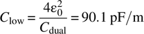
Figure 15.2 shows a quarter section of a square within a square. This is the same example that was used in Chapter 10. The gmsh coding for this consists simply of the six-sided polygon shown in Figure 15.2; there are no excluded interior regions.
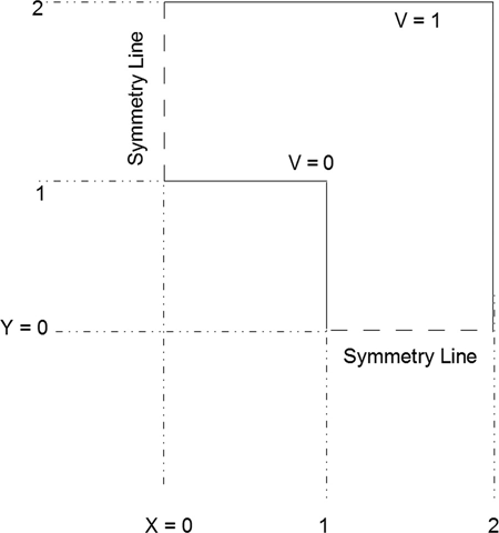
FIGURE 15.2 Sample structure with two symmetry lines.
The first code modifications needed are to parse_msh_file.m. As written, parse_msh_file.m considered only conductor boundaries that were closed polygons. In this situation a full list of the nodes containing the endpoints of all the line segments would contain each node twice (once on each end of each line segment). To avoid this redundancy, only one end of the line was examined for its node number.
As Figure 15.2 shows, we now have to consider some nodes that form the junction of a conductor and a symmetry line — with the boundary condition (bc) on the conductor taking precedence. Adding one extra line after line 77 accomplishes this task. When a structure contains connected conductor line segments, the program does generate some redundant information. This information doesn't cause any trouble, so to keep things as simple as possible, no extra code was written to “search and destroy” these extra lines.
Next, we need a way to explain our new bc information to the programs. In Problem 14.4, this was done by manually editing the bcs file. This time we'll update the parse_msh_file program to add this capability.
The bc data entry system is now as follows:
- The program will loop through all of the defined lines of the structure.
- For each line, set any desired bc voltage except -
9999, which will be used as a flag to indicate a line of symmetry.
MATLAB program parse_mesh_file2.m is as follows:
% parse_msh_file2.m
% Read the mesh file generated by gmsh and parse it
% This is a very limited routine, based only on the
%  capabilities of gmsh that are being used
% This is an extension parse_msh_file.m, to allow for symmetries

%  Element types handled are 1 = line, 2 = 3 node triangle, 15 = point

 filename = uigetfile('*.msh'),      % read the file
 fid = fopen(filename, 'r'),

 tline = fgetl(fid);             % read the first file line
 if (strcmp(tline, '$MeshFormat')) == 0  % Verify file type
  'Problem with this file'
  nodes = []; trs = []; bcs = [];
  fclose (fid);
  return
 end

 tline = fgetl(fid);            % look for version number
 [header] = sscanf(tline, '%f %d %d'),
 if (header(1) ~ = 2.2), 'Possible gmsh version incompatibility', end;

 tline = fgetl(fid);            % Look for $EndMeshFormat
 if (strcmp(tline, '$EndMeshFormat')) == 0
  'No $EndMeshFormat Line found'
  nodes = []; trs = []; bcs = [];
  fclose (fid);
  return
 end

 tline = fgetl(fid); % Look for $Nodes
 if (strcmp(tline, '$Nodes')) == 0
  'No $Nodes Line found'
  nodes = []; trs = []; bcs = [];
  fclose (fid);
  return
 end

 % NOTE: Nodes is being read as a 3-d file even though only 2-d
 %     usage is anticipated in this version

 nr_nodes = fscanf(fid, '%d', 1);     % get number of nodes
 nodes = [0,0,0]; % zeros(nr_nodes, 3);  % allocate nodes array
 for i = 1 : nr_nodes % get nodes information
  temp = fscanf(fid, '%g', 4);
  n = temp(1);
  nodes(n,:) = temp(2:4);
 end
 fgetl(fid);             % Clear the line

 tline = fgetl(fid); % Look for $EndNodes
 if (strcmp(tline, '$EndNodes')) == 0
  'No $EndNodes Line found'
  nodes = []; trs = []; bcs = [];
  fclose (fid);
  return
 end

 tline = fgetl(fid);              % Look for $Elements
 if (strcmp(tline, '$Elements')) == 0
  'No $Nodes Line found'
  nodes = []; trs = []; bcs = [];
  fclose (fid);
  return
 end

 trs = []; bcs = [];
 nr_elements = fscanf(fid, '%d', 1); % get number of elements
 for i = 1: nr_elements % process elements information
  temp = fscanf(fid, '%d %d', 2);  % get element type
  if temp(2) == 15 % defined point
   fgetl(fid); % clear the line
  elseif temp(2) == 1 % defined line
   temp2 = fscanf(fid, '%d %d %d %d %d', 5);
   bcs = [bcs; [temp2( 3:4)', 0]];

%  --------------------------------------------------
%  added line for symmetry calcs - get both nodes on bc line
%  this adds some redundancy to the bcs file, but no harm
   bcs = [bcs; [temp2(3), temp2(5), 0]];
%  --------------------------------------------------

   fgetl(fid);
  elseif temp(2) == 2 % created mesh triangle
   temp3 = fscanf(fid, ' %d  %d  %d  %d  %d  %d', 6);
   if temp3(3) < 200 % ignore excluded triangles
    trs = [trs; temp3(4:6)'];
   end
   fgetl(fid);
  else
   'Unknown type in mesh file'
   nodes = []; trs = []; bcs = [];
   fclose (fid);
   return
  end
 end
 fclose (fid);

 nr_bc_lines = length(bcs);
 'bcs file: '
 bcs
 % ----- modified lines for symmetry calculations ---------------
 disp ('Set bcs for all lines, -9999 for symmetry line'),
 while 1 == 1
  line_nr = input('Enter line nr for bc: ')
   if line_nr == 0, break; end;
   j = input('Enter bc: ')             % decide on the bc
   for k = 1 : nr_bc_lines              % set the bc
    if bcs(k,1) == line_nr, bcs(k,3) = j; end;
   end
  'bcs file: '
  bcs
 end
 % ----------------------------------------------------------------

 filename = input('Name for output files, NO OVERWRITE CHECKING: ', 's'),
 nodes_file_name = strcat('nodes_', filename, '.txt'),
 trs_file_name = strcat('trs_', filename, '.txt'),
 bcs_file_name = strcat('bcs_', filename, '.txt'),
 fid = fopen (nodes_file_name, 'w'),
 fprintf (fid, '%g	%g	%g
', nodes'),
 fclose (fid);
 fid = fopen (trs_file_name, 'w'),
 fprintf (fid, '%d	%d	%d
', trs'),
 fclose (fid);
 fid = fopen (bcs_file_name, 'w'),
 fprintf (fid, '%d	%d	%d
', bcs'),
 fclose (fid);
Program parse_msh_file2.m is the revised version of this program.
Next, fem_2d.1.m must be modified to properly deal with the new information. The changes are so minor that the revised programs need not be fully listed. These changes are as follows:
-
In
fem_2d_1.m, in the section beginning with the comment line%bcs, change theifstatement toifbcs.volts(i) ~ = -9999 % symmetry axis = -9999 - In
show_mesh.m, change the line before thetextcommand to the same as above.
The first change above causes the FEM analysis to not set up any boundary conditions at edges specified as boundary conditions; in other words, just ignore them, as explained above. Edges are treated the same as internal nodes.
The second change above does the same for the show_mesh routine.
Referring to Figure 15.2, number the lines counterclockwise, beginning with the symmetry line at Y = 0. The responses to the bcs prompt in (the modified version of) show_mesh.m are then -9999, 1, 1, -9999, 0, and 0.
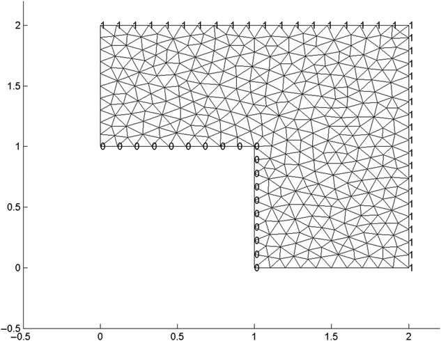
FIGURE 15.3 Structure shown in Figure 15.2 after meshing.
Figure 15.3 shows the same structure, including the meshing; Figure 15.4 shows the voltage distribution of the structure; and Figure 15.5 shows the electric field distribution.
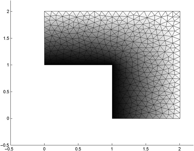
FIGURE 15.4 Structure from Figure 15.2 showing voltage distribution.
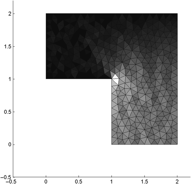
FIGURE 15.5 Structure from Figure 15.2 showing field distribution.
The calculated capacitance of the structure is 4(22.77) = 91.1 pF/M. As mentioned in Chapter 10, the exact capacitance of this structure is 90.6 pF/M. This FEM result is 0.5% high. This structure was zoned with 385 nodes, a fairly low-resolution zoning.
As was discussed in Section 9.7, the dual capacitance may be found by reversing the fixed and symmetry boundary lines. For this same structure (and same mesh file), this means that the bc responses to parse_msh_file.m are 0, -9999, -9999, 1, -9999, and -9999.
Examination of the figures produced by fem_2d_1.m show that the program has correctly interpreted the boundary conditions and is producing reasonable looking voltage and field distributions.
The capacitance produced by the program is C dual = 3.48. Using equations (9.27) and (9.28) to calculate the electrical low-capacitance estimate, we obtain
This capacitance is 0.5% lower than the exact value. As discussed in Chapter 9, the best estimate is obtained by averaging the high- and low-capacitance estimates; the result is essentially the exact answer.
At this point the value of FEM modeling is becoming apparent. The ability to represent arbitrary structures and the ability to easily apply different boundary conditions clearly separates it from the FD and MoM techniques. Although FEM programs are more involved than either FD or MoM programs, from a user’s perspective they are much more flexible.
Figure 15.6 shows another example of the flexibility of the FEM calculation.
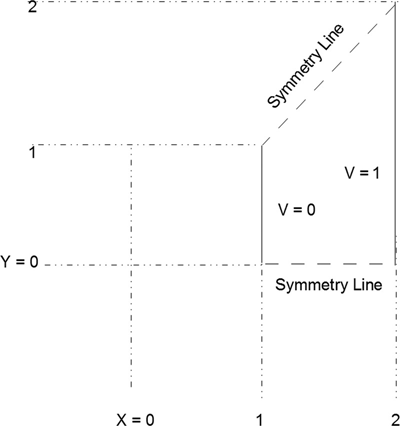
FIGURE 15.6 Structure with eightfold symmetry.
Figure 15.6 shows the same structure as in the previous example, but in this case only ![]() th of the total square conductors is shown. The line from (1,1) to (2,2) is also a line of symmetry, or magnetic wall. It does not matter that the line is not parallel to either the X or the Y axis.
th of the total square conductors is shown. The line from (1,1) to (2,2) is also a line of symmetry, or magnetic wall. It does not matter that the line is not parallel to either the X or the Y axis.
Both fem_2d_1.m and parse_msh_file1.m, including the modifications described above, treat this geometry correctly and produce good results for both the physical and the dual-structure capacitances, again with excellent accuracy for the average of the two capacitances, using only a modest number of nodes.
15.3 Axisymmetric Structures
An axisymmetric structure is a structure that has cylindrical symmetry. The geometry is described, in cylindrical coordinates, in terms of r and z only — there are no angular variations. Since there are only two variables involved, these structures may be zoned in the same manner as 2d rectangular problems, but the interpretation of the drawing is very different.
For example, consider the example used in Section 15.2 (Figures 15.2 and 15.6). These figures described the cross section of an infinitely long (in z) pair of concentric squares. Figure 15.7 shows the various ways this structure may be zoned, either using the full cross section (a) or taking advantage of various axes of symmetry (b), (c), and (d).
FIGURE 15.7 Cross section choices for concentric square transmission line: (a) Full cross section: (b)  symmetry; (c)
  symmetry; (d)
  symmetry.
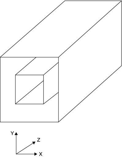
FIGURE 15.8 Perspective view of concentric square transmission line.
Figure 15.8 shows a perspective view of the same concentric square transmission line. An important point to keep in mind here is that Figure 15.8 does not show the entire structure described. It just shows a section (in z) of the structure. The structure is infinitely long in Z, and we have been dealing only with a cross section of it. Since such a structure with no Z dependence (i.e., uniform) can be described entirely by voltages and fields that are only functions of X and Y, a 2d analysis finds everything there is to know about the structure. Voltages, electric field components and energy density are functions of X and/or Y only and are valid for any value of Z. Total energy and capacitance values are calculated as joules and farads per unit length.
Now consider Figure 15.9.
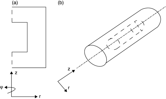
FIGURE 15.9 (a) Cross section between r and z and (b) perspective view of concentric cylinder structures.
Figure 15.9a is identical to Figure 15.7b except that the axes are now labeled (r,z) rather than (x,y). The structures represented, however, are not the same. Figure 15.9b shows the axisymmetric structure described by Figure 15.9a. There are two important points to make here:
- Figure 15.9 shows the entire structure being modeled, not just a piece of it. It is a 3d structure shown in its entirety with both cylinders shorted at both ends. The capacitance between the inner and outer cylinders and the total stored energy (for some prescribed electrode voltages) are measured in farads and joules, respectively.
- The location of z = 0 for the structure is arbitrary, as is the location of x = 0 and y = 0 in rectangular coordinates insofar as the properties of the structure are concerned. In other words, Figure 15.9b may be moved (caused to slide) up or down the z axis without changing any structure properties. On the other hand, the r axis is fixed. In order to retain the axisymmetric status, there can be no ϕ dependence, and the structure in Figure 15.9b must always be fully describable by its cross section (Figure 15.9a).
Deriving the formulas for the coefficient matrix for an axisymmetric structure using triangles with the shape functions defined in Chapter 13 duplicates the analysis of Chapter 13, except that X is replaced with r and Y is replaced with z, up to the energy expression [equation (13.10)]:
As in this equation, the energy is constant over the triangle. The integral, over the area of the triangle, however, is now
Evaluating the integral in equation (15.3) is not a trivial task. Fortunately, it is an already accomplished and well-documented task. If we put aside the physics behind equation (15.3) and look only at the integral
we recognize this integral as the X component of the center of mass of an arbitrary triangle T in the X–Y plane.
The solution to this, as documented in many places,2–4 is
where AT is the triangle’s area, as before, and rc is the average of the three nodes' r values:
Modifying the MATLAB code to study axisymmetric problems is very simple:
- When calculating the coefficient matrix, simply multiply the area by rc . In the code below, this multiplication is carried out every time AT is used rather than before it is used. This is unnecessary, but hopefully the clearest way to present this change.
- When calculating the capacitance, multiply the area by rc , as above, and then multiply by an additional 2π, the integral over φ. This latter multiplication was not needed in the coefficient term calculation because, being the same for all terms, it drops out.
The MATLAB listings below show the code, including both the earlier changes in this chapter and the calculations corrected for axisymmetric structures:
-
MATLAB program
fem_2d.3.m— MATLAB script for FEM modeling of axisymmetric structures:% 2d FEM with triangles % fem_2d_3.m is for axisymmetric structures % This includes all the modifications to fem_2d_1.m to handle symmetries % Just to avoid rewriting a lot of code, nodes are referred to as x & y % These should be interpreted as r and z, respectively close filename = input('Generic name for input files: ', 's'), nodes_file_name = strcat('nodes_', filename, '.txt'), trs_file_name = strcat('trs_', filename, '.txt'), bcs_file_name = strcat('bcs_', filename, '.txt'), % get node data from file dataArray = load(nodes_file_name); nds.x = dataArray(:,1); nds.y = dataArray(:,2); nds.z = 0; nr_nodes = length(nds.x) % get triangles data from file trs = (load(trs_file_name))'; nr_trs = length(trs) % get bcs data from file dataArray = load(bcs_file_name); bcs.node = dataArray(:,2); bcs.volts = dataArray(:,3); nr_bcs = length(bcs.node) % allocate the matrices a = sparse(nr_nodes, nr_nodes); f = zeros(nr_nodes,1); b = zeros(3,nr_nodes); c = zeros(3,nr_nodes); % generate the matrix terms d = ones(3,3); for tri = 1: nr_trs % Walk through all the triangles n1 = trs(1,tri); n2 = trs(2,tri); n3 = trs(3,tri); d(1,2) = nds.x(n1); d(1,3) = nds.y(n1); d(2,2) = nds.x(n2); d(2,3) = nds.y(n2); d(3,2) = nds.x(n3); d(3,3) = nds.y(n3); Area = det(d)/2; rc = (nds.x(n1) + nds.x(n2) + nds.x(n3))/3.; temp = d[1; 0; 0]; b(1,tri) = temp(2); c(1,tri) = temp(3); temp = d[0; 1; 0]; b(2,tri) = temp(2); c(2,tri) = temp(3); temp = d[0; 0; 1]; b(3,tri) = temp(2); c(3,tri) = temp(3); a(n1,n1) = a(n1,n1) + rc*Area*(b(1,tri)^2 + c(1,tri)^2); a(n1,n2) = a(n1,n2) + rc*Area*(b(1,tri)*b(2,tri) + c(1,tri)*c(2,tri)); a(n1,n3) = a(n1,n3) + rc*Area*(b(1,tri)*b(3,tri) + c(1,tri)*c(3,tri)); a(n2,n2) = a(n2,n2) + rc*Area*(b(2,tri)^2 + c(2,tri)^2); a(n2,n1) = a(n2,n1) + rc*Area*(b(2,tri)*b(1,tri) + c(2,tri)*c(1,tri)); a(n2,n3) = a(n2,n3) + rc*Area*(b(2,tri)*b(3,tri) + c(2,tri)*c(3,tri)); a(n3,n3) = a(n3,n3) + rc*Area*(b(3,tri)^2 + c(3,tri)^2); a(n3,n1) = a(n3,n1) + rc*Area*(b(3,tri)*b(1,tri) + c(3,tri)*c(1,tri)); a(n3,n2) = a(n3,n2) + rc*Area*(b(3,tri)*b(2,tri) + c(3,tri)*c(2,tri)); end %bcs for i = 1: nr_bcs if bcs.volts(i) > = 0 n = bcs.node(i); a(n,:) = 0; a(n,n) = 1; f(n) = bcs.volts(i); end end % fake bcs for nodes in excluded region - assuming boundary at 1 volt % There might not be any excluded regions in symmetry problems % This is being left for backwards-compatibility of the program for i = 1 : nr_nodes if a(i,i) == 0 a(i,:) = 0; a(i,i) = 1; f(i) = 1; end end v = af; % plot the mesh show_mesh2(nr_nodes, nr_trs, nr_bcs, nds, trs, bcs, v) % calculate capacitance C = get_tri2d_cap_2(v, nr_nodes, nr_trs, nds, trs) % show field profile get_tri2d_E_2(v, nr_nodes, nr_trs, nds, trs) % show voltage along chosen edge x_temp = []; v_temp = []; for i = 1 : nr_nodes % if abs(nds.y(i)) < .1 %nds.y(i) == 0 if nds.x(i) < .01 & nds.y(i) > = 0 %nds.y(i) == 0 % fprintf ('%d %d %f ', i, nds.y(i), v(i)) x_temp = [x_temp, nds.y(i)]; v_temp = [v_temp, v(i)]; end end %x_temp = sort(x_temp); %v_temp = sort(v_temp); v_exact = -log(x_temp)/log(2) + 1; % v_exact = x_temp - 1; figure(4) %plot(x_temp, v_temp, '.r', x_temp, v_exact, 'x') plot(sort(x_temp), sort(v_temp), 'k') -
MATLAB program
get_tri2d_cap_2.m—MATLAB function for capacitance of axisymmetric structures:function C = get_tri2d_cap_2(v, nr_nodes, nr_trs, nds, trs) % Calculate the capacitance of a 2d triangular structure % Simple linear approx. function is assumed % This version is for axisymmetric structures eps0 = 8.854; U = 0; d = ones(3,3); for tri = 1 : nr_trs n1 = trs(1,tri); n2 = trs(2,tri); n3 = trs(3,tri); d(1,2) = nds.x(n1); d(1,3) = nds.y(n1); d(2,2) = nds.x(n2); d(2,3) = nds.y(n2); d(3,2) = nds.x(n3); d(3,3) = nds.y(n3); temp = (d[1; 0; 0]); b1 = temp(2); c1 = temp(3); temp = (d[0; 1; 0]); b2 = temp(2); c2 = temp(3); temp = (d[0; 0; 1]); b3 = temp(2); c3 = temp(3); Area = det(d)/2; if Area < = 0, disp 'Area < = 0 error'; end; rc = (d(1,2) + d(2,2) + d(3,2))/3; U = U + 2*pi*rc*Area*((v(n1)*b1 + v(n2)*b2 + v(n3)*b3)^2 ⋯ + (v(n1)*c1 + v(n2)*c2 + v(n3)*c3)^2); end U = U*eps0/2; C = 2*U; % Potential difference of 1 volt assumed end -
MATLAB program get_tri2d_E_2.m—MATLAB function for E field distribution in axisymmetric structures:
function get_tri2d_E(v, nr_nodes, nr_trs, nds, trs)
% Calculate and show the field magnitude profile
% E_mag calculation is identical to that in capacitance calculation
% function

eps0 = 8.854;

d = ones(3,3); E_mag = zeros(nr_trs,1);
for tri = 1 : nr_trs
  n1 = trs(1,tri); n2 = trs(2,tri); n3 = trs(3,tri);
  d(1,2) = nds.x(n1); d(1,3) = nds.y(n1);
  d(2,2) = nds.x(n2); d(2,3) = nds.y(n2);
  d(3,2) = nds.x(n3); d(3,3) = nds.y(n3);
  temp = (d[1; 0; 0]); b1 = temp(2); c1 = temp(3);
  temp = (d[0; 1; 0]); b2 = temp(2); c2 = temp(3);
  temp = (d[0; 0; 1]); b3 = temp(2); c3 = temp(3);

  % Use these two lines to look at E_magnitude
  E_mag(tri) = ((v(n1)*b1 + v(n2)*b2 + v(n3)*b3)^2 ⋯
     + (v(n1)*c1 + v(n2)*c2 + v(n3)*c3)^2);

  % Use these two lines to only look at Ex
  % E_mag(tri) = eps0/2*(v(n1)*b1 + v(n2)*b2 + v(n3)*b3)^2;

  % Use these two lines to only look at Ey
  % E_mag(tri) = eps0/2*(v(n1)*c1 + v(n2)*c2 + v(n3)*c3)^2;

end
E_peak = max(E_mag)

E_mag = sqrt(E_mag/max(E_mag)); % normalize

figure(3)

x_min = min(nds.x)*1.1;
if x_min == 0, x_min = -.5; end;
x_max = max(nds.x)*1.1;
y_min = min(nds.y)*1.1;
if y_min == 0, y_min = -.5; end;
y_max = max(nds.y)*1.1; axis ([x_min, x_max, y_min, y_max]);
axis ([x_min, x_max, y_min, y_max]);
axis square;
hold on

for tri = 1 : nr_trs
  n1 = trs(1,tri); n2 = trs(2,tri); n3 = trs(3,tri);
  x = [nds.x(n1); nds.x(n2); nds.x(n3)];
  y = [nds.y(n1); nds.y(n2); nds.y(n3)];
  E = [E_mag(tri); E_mag(tri); E_mag(tri)];
  fill(x,y,E)
end
A very simple example of an asymmetric structure is shown in Figure 15.10.
FIGURE 15.10 Infinite-length concentric cylinder structure.
Figure 15.10 shows two concentric cylinders, of radii 1 and 2. They are both 1 unit long, centered at z = 0. The use of symmetric planes at z = -0.5 and z = 0.5 means that the FEM calculation is effectively for a pair of infinitely long concentric cylinders. In other words, while we previously had been using a 2d cross section calculation to model uniformly infinitely long structures, now we are using an axisymmetric 3d calculation to do the same thing. This example adds nothing to our solution capability, but is instructional as to setting up structures for the axisymmetric calculation. Program struct15_1.geo—the gmsh file for the structure in Figure 15.10—is very simple:
// Structure file struct15_1.geo
// Symmetric coaxial line for 3d calc

lc = .05;

Point(1) = {1, -.5, 0, lc};
Point(2) = {2, -.5, 0, lc};
Point(3) = {2, .5, 0, lc};
Point(4) = {1, .5, 0, lc};

Line(1) = {1, 2};
Line(2) = {2, 3};
Line(3) = {3, 4};
Line(4) = {4, 1};

// exterior surface
Line Loop(1) = {1, 2, 3, 4};
Plane Surface(2) = {1} ;
For this gmsh file, the bc prompts in parse_msh_file2.m are -9999, 0, -9990, and 1.
Program fem_2d.3.m calculates the capacitance of this structure to be 80.266 pF/m. The exact capacitance, as derived in Chapter 13, is
This FEM calculation, with a 530-node, 980-triangle structure, predicts the capacitance with an error of 0.01%.
The gmsh file struct15_2.geo—using parametric data—creates the structure shown and discussed in Figures 15.11–15.13:
// structure file struct15_2.geo
// Finite length concentric cylinders

lc = .1;

h = 0.6;  // overall structure 1/2 height
t = 0.5;  // end cap thickness
h2 = h - t;
ra = 1;  // inner radius
rb = 2;  // outer radius

// exterior loop
Point(1) = {0, -h, 0, lc};
Point(2) = {rb, -h, 0, lc};
Point(3) = {rb, h, 0, lc};
Point(4) = {0, h, 0, lc};
Point(5) = {0, h2, 0, lc};
Point(6) = {ra, h2, 0, lc};
Point(7) = {ra, -h2, 0, lc};
Point(8) = {0, -h2, 0, lc};

Line(1) = {1, 2};
Line(2) = {2, 3};
Line(3) = {3, 4};
Line(4) = {4, 5};
Line(5) = {5, 6};
Line(6) = {6, 7};
Line(7) = {7, 8};
Line(8) = {8, 1};

// exterior surface
Line Loop(1) = {1, 2, 3, 4, 5, 6, 7, 8};
Plane Surface(2) = {1} ;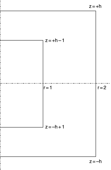
FIGURE 15.11 Structure defined using struct15_2.geo.
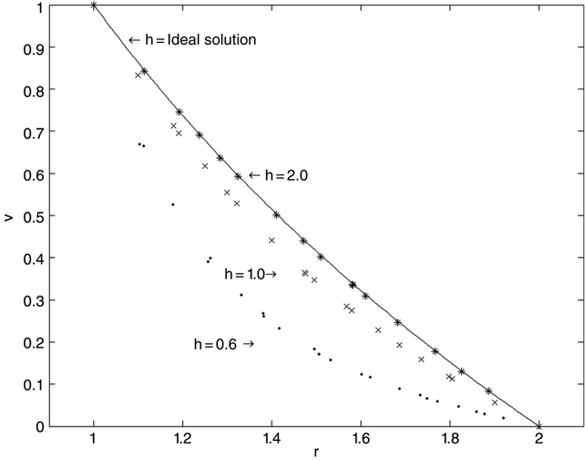
FIGURE 15.12 Results of FEM analysis of struct8.geo.
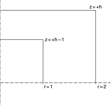
FIGURE 15.13 Structure from Figure 15.11 showing Z symmetry.
This file introduces a very convenient capability of gmsh, namely, the ability to perform calculations using defined variables, and refer to these variables for structural information. These variables are defined schematically in Figure 15.11.
Referring to Figure 15.11, when h is very large as compared to ra, rb, and t, we expect the voltage profile near z = 0 to approximate the voltage profile between two infinitely long cylinders, as calculated in Chapter 10:
Figure 15.12 shows a plot of equation (15.8) and data for the FEM analysis of struct15_2.geo, using three different values of h. All other values are kept constant as in struct15_2.geo. When h = 0.8, the voltage profile looks nothing like the analytic solution except, of course, that the boundary conditions are satisfied. When h = 1.0, the voltage profile approximates the analytic solution. When h = 2.0, the voltage profile is indistinguishable from the analytic solution. The value of the ability to set parametric values in gmsh and then vary them to perform parameter studies on a given structure is considerable. To be complete, we should vary the resolution and make sure that it is high enough to ensure that the results are due to the fact that the parameters are deliberately varied and not noticeably due to subtle changes in zoning when a parameter is changed.
Figure 15.13 is a repeat of the structure of Figure 15.11, but only the z ≥ 0 region is shown. The value Z = 0 is an axis of symmetry (along with r = 0), and the FEM analysis may be run this way. The results, of course, will be identical to these results.
Again, note that in axisymmetric structures z-axis symmetries behave correctly. The r = 0 symmetry is necessary, but no other r-axis symmetries are meaningful.
15.4 The Graded-Potential Boundary Condition
A situation often encountered in electrostatic analysis is an axisymmetric structure where the outer boundary bc is a potential that is graded (typically linearly) between two defined points. An example of such a structure is shown in Figure 15.14, showing a simplified cross section of a cathode ray tube (CRT). For about 50 years, before the advent of liquid crystal display (LCD) displays, the CRT was the mainstay of the television, oscilloscope, and (in the later years) the computer monitor industries.
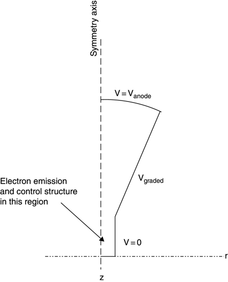
FIGURE 15.14 A simplified CRT outline.
A CRT is built using a sealed glass package, under high vacuum. The base of the package (near z = 0 in the figure) holds an electron emitter structure and control electrodes; these are not shown in this figure. The sidewalls of the package are coated with a highly resistive material so that voltages may be applied but very little current will flow. The sidewall tapers out (in r) from the base to the anode, or screen, of the CRT. The screen is coated with phosphor materials (materials that emit light when struck by energetic electrons). The screen is set to a high voltage, typically ~15 kV.
The tapered sidewall of the package is set to a linearly graded voltage that is equal to 0 at the base and equal to the anode voltage at the anode. Electrons that have been emitted into the vacuum and aimed at particular locations on the anode (the screen) accelerate through the (approximately) uniform field of the graded region and strike the anode.
Incorporating the capability of setting one or more lines to a graduated voltage may be accomplished by modifying parse_msh_file2.m, modifying fem_2d_3.m, or adding a new and separate MATLAB script that the bc data file must be run through. This latter approach was chosen, not because of any performance incentives, but in the interest of keeping each piece of code as clear and unentangled as possible.
MATLAB program graded_bc.m is as follows:
% graded_bc.m A short script to apply a graded boundary condition to an
% existing bc_XXX.txt file

filename = input('Generic name for input files: ', 's'),
bcs_file_name = strcat('bcs_', filename, '.txt'),
nodes_file_name = strcat('nodes_', filename, '.txt'),

bcs = load(bcs_file_name);
nds = load(nodes_file_name);

line_nr = 8888;  % get input information
while line_nr ~ = 0
  bcs
  line_nr = input('Enter line number for graded bc, 0 to terminate: '),
  if line_nr == 0
   break
  end
  v1 = input('Enter starting voltage ')
  v2 = input ('Enter ending voltage ')

  % find the line number and get the start and stop points in the file
  for i = 1 : length(bcs)
   if bcs(i,1) == line_nr
    p1 = bcs(i,2); % start point
    break
   end
  end
  p2 = bcs(length(bcs),2);
  for j = i + 1 : length(bcs)
   if bcs(j,1) ~ = line_nr
    p2 = bcs(j-1,2); % stop point
    break
   end
  end

  % get the length of the line
  line_length = sqrt((nds(p1,1) - nds(p2,1))^2 + (nds(p1,2) - nds(p2,2))^2);

  for i = 1 : length(bcs) % scale the voltage by length along the
   if bcs(i,1) == line_nr % chosen line and set the bc
    p = bcs(i,2);
    bcs(i,3) = v1 + (v2-v1)*sqrt((nds(p,1) - nds(p1,1))^2 ⋯
     + (nds(p,2) - nds(p1,2))^2)/line_length;
   end
  end
end

% replace the bcs file on disk
save (bcs_file_name, 'bcs', '-ascii')
Program graded_bc.m should be run after the parse_msh_file2.m has been run for a given dataset. In parse_msh_file2.m, the line whose bc is to be graded may be set to any convenient, temporary, value (0 is fine). Program graded_bc.m will prompt for a line (or lines) to grade and then ask for starting and stopping voltages for the gradation.
(Important note: Program graded_bc.m does not perform any validity checking on the entered data. A line with voltage graded between, say, 0 and 100-V should connect to a 0-V bc line at its beginning and to a 100-V bc line at its end. Any other conditions are not physical and will lead to useless results in the FEM analysis.)
The gmsh structure file struct15_3.geo—file for the CRT profile—is presented here:
// structure file struct15_3.geo
// Simple cylinder for demonstrating bias capability

lc = .5;

// exterior loop
Point(1) = {0, 0, 0, lc};
Point(2) = {1, 0, 0, lc};
Point(3) = {1, 2, 0, lc};
Point(4) = {5, 10, 0, lc};
Point(5) = {0, 11., 0, lc};

Point(6) = {0, -.5, 0, lc}; // circle center point

Line(1) = {1, 2};
Line(2) = {2, 3};
Line(3) = {3, 4};
Circle(4) = {4, 6, 5};
Line(5) = {5, 1};

// exterior surface
Line Loop(1) = {1, 2, 3, 4, 5};
Plane Surface(2) = {1} ;
The gmsh file struct15_3.geo generates the CRT outline structure shown in Figure 15.14. Using parse_msh_file2.m to set the fixed boundary conditions of 0 V everywhere except at the screen, 100 V at the screen; and then using graded_bc.m to set a linear taper from the base (neck) of the CRT to the screen, we get the FEM analysis model shown in Figure 15.15. Remember that the line at r = 0 with no bc numbers in this figure denotes the axisymmetric r = 0 boundary condition. Also, as may be seen, a relatively coarse meshing grid is shown; the intent is to demonstrate the file generation procedure and not to strive for a very accurate result.
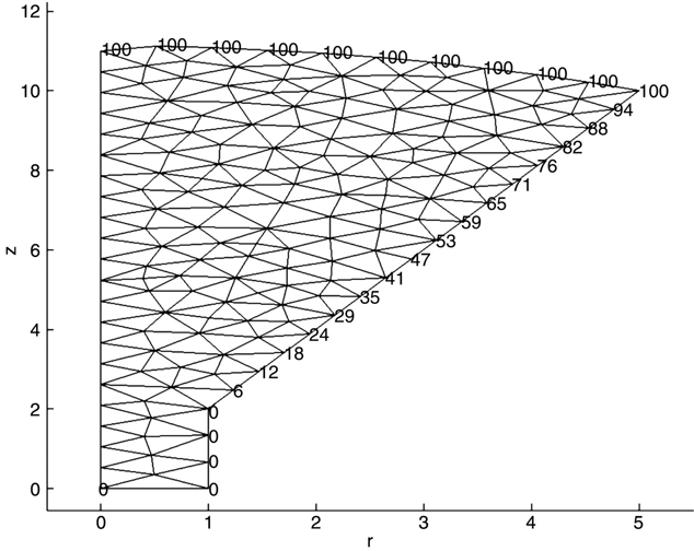
FIGURE 15.15 fem_2d.3.m figure showing CRT boundary condition setup.
Figure 15.16 shows the voltage profile along the r = 0 axis for the CRT structure.
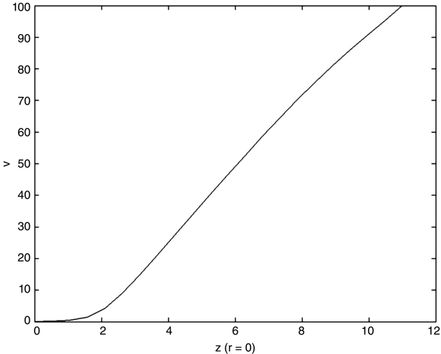
FIGURE 15.16 The r = 0 voltage profile for CRT FEM model.
The voltage profile shows that the neck of the CRT is essentially a field-free region; the voltage increases approximately linearly with z between z = 2 and the screen.
15.5 Unbounded Regions
[Note: In this section we are no longer considering axisymmetric structures. We are (back) to 2d rectangular cross sections of uniform infinite (in z) structures. The MATLAB scripts and functions for the rectangular and axisymmetric cases are not very different — care should be taken that the correct programs are being used because the results are very different and using the wrong program will result in nonsensical (if any) results.]
Many structures are not well described as a layout with an enclosing boundary. In the physical world no structure is infinitely far away from everything else, but often the best physical approximation is that this structure is alone in the universe. Figure 15.17 is an example of such a structure.
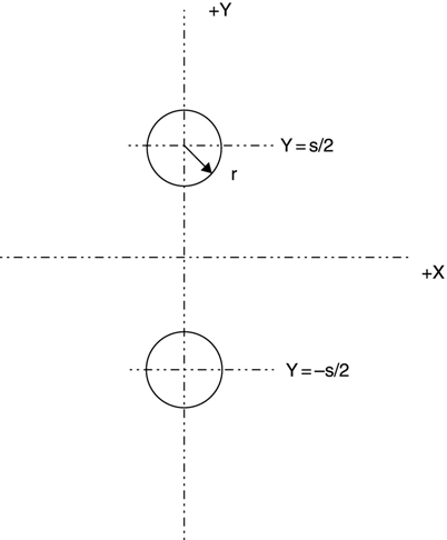
FIGURE 15.17 Cross section of a parallel wire transmission line.
Figure 15.17 shows the cross section of a parallel wire transmission line. In practice, these lines are built using periodic insulators to support the structure or the lines are embedded into a flat plastic continuous insulator. The latter structure is the 300-Ω twin lead brown TV antenna line that dominated home TV installations for many years. The former structure was popular for many years in open installations, such as antennas on large ships (before the advent of good low-loss dielectric materials) because it was the lowest-loss transmission line available.
The structure of Figure 15.17 is idealized in that there is no mechanical support. It is a good example for studying approximate analysis techniques because the exact capacitance (and hence transmission line parameters) may be calculated.5 For s = 3 and r = 0.5, we obtain
If we model this structure setting the electrodes at 0.5 and -0.5 V then we still maintain the convenience of dealing with a 1-V difference between the electrodes, and also since the average value of the voltages is zero, we can expect the voltage at infinity to be zero (see Chapter 3 for further discussion of this issue).
If we now want to build an FEM mesh to model this structure, we immediately see our problem — we need to create a mesh encompassing all space. This is clearly not a realistic task.
If the voltage goes to zero at infinity and we have centered our structure at or near the origin, then we should be able to create a v = 0 circular boundary far enough from the origin. This would give us a finite region to build a mesh. The question, of course, is what exactly — is meant by “far enough.”
The ghmsh program struct15_4.geo—showing a parallel wire line region with a circular boundary creates just this situation:
// structure file struct15_4.geo
// First program for setting up semi-infinite boundaries

lc = 1.;

// outer circle
rout = 6;

Point(10) = {rout, 0.0, 0, lc};
Point(11) = {0.0, 0.0, 0, lc};
Point(12) = {0.0, rout, 0, lc};
Point(13) = {-rout, 0.0, 0, lc};
Point(14) = {0, -rout, 0, lc};

Circle(20) = {10, 11, 12};
Circle(21) = {12, 11, 13};
Circle(22) = {13, 11, 14};
Circle(23) = {14, 11, 10};

sep = 3;
rin = 0.5;
// upper inner circle
Point(30) = {rin, sep/2, 0, lc};
Point(31) = {0, rin + sep/2, 0, lc};
Point(32) = {-rin, sep/2, 0, lc};
Point(33) = {0, sep/2-rin, 0, lc};
Point(34) = {0, sep/2, 0, lc};

Circle(40) = {30, 34, 31};
Circle(41) = {31, 34, 32};
Circle(42) = {32, 34, 33};
Circle(43) = {33, 34, 30};
Line Loop(44) = {40, 41, 42, 43};
//Plane Surface(45) = {44};

// lower inner circle
Point(50) = {rin, -sep/2, 0, lc};
Point(51) = {0, rin-sep/2, 0, lc};
Point(52) = {-rin, -sep/2, 0, lc};
Point(53) = {0, -sep/2-rin, 0, lc};
Point(54) = {0, -sep/2, 0, lc};

Circle(60) = {50, 54, 51};
Circle(61) = {51, 54, 52};
Circle(62) = {52, 54, 53};
Circle(63) = {53, 54, 50};

Line Loop(64) = {60, 61, 62, 63};
//Plane Surface(65) = {64};
Line Loop(24) = {20, 21, 22, 23};
Plane Surface(25) = {24, 44, 64};
The proper boundary conditions for this structure are 0.5 and -0.5 V for the inner circles and 0 V for the outer circle.
Figure 15.18 shows the results of this exercise.
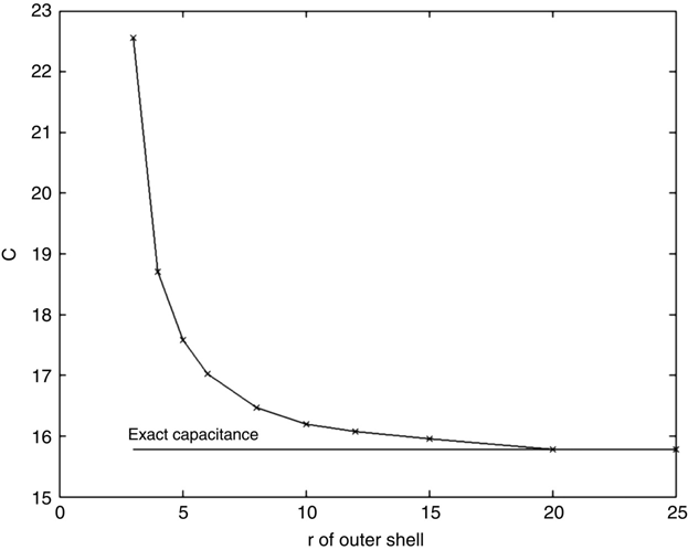
FIGURE 15.18 FEM analysis of parallel wire line versus outside boundary circle radius.
At an outer boundary shell radius of approximately ≥20, the predicted capacitance is essentially the exact capacitance. The procedure works well, but its practicality is questionable. Simply increasing the outer shell increases the size of the coefficient matrix rapidly. Since this example was simply two circles, the necessary resolution was modest. If a more complex structure was involved and higher resolution was needed, this process could be impractical. Some other approaches are needed.
Chari and Salon present a survey of various techniques developed to deal with unbounded, or open bounded regions.6 Simplified versions of two of these techniques will be presented here.
Figure 15.19 shows a section of the outer region of the structure described above (struct15_4.geo). The outer circle radius is R. One triangle with two nodes on the outer circle at voltages Va
and Vb
is shown. This figure is exaggerated for clarity. The outer circle in an actual structure with a reasonable resolution mesh would be much closer to the outer triangle line than the figure implies.
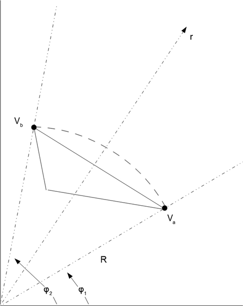
FIGURE 15.19 Section of struct15_4.geo near the outer circle.
Experience tells us that once we're a reasonable distance from an electrically neutral structure (such as our parallel wire line example), the voltage profile from a circle surrounding this structure out to infinity is not a very interesting function. There will be a an angular dependence (the angle from the X axis to a line from the origin to a field point), just as there is an angular dependence of the electric dipole voltage profile far from the dipole itself. Also, the voltage will have to fall off at least as rapidly as it does in the case of the electric dipole, that is, with the square of the distance from the origin.
In Figure 15.19, two lines from the origin (the center of the circle) have angles φ1 and φ2 with respect to the X axis, as shown.
Since Vb and Va cannot be too different, and since the arc of the circle is close to the line connecting nodes a and b, we will approximate the voltage on the circle arc between these two nodes as follows:
Then, for r ≥ R, we let
We have now created a new element for our structure. This element is bounded by the arc r = R and the lines φ1 and φ2. It is unbounded as r goes to infinity. The voltage profile chosen [equation (15.11)] ensures that the energy in the region is finite. This voltage profile is also the voltage profile of an electric dipole (see Chapter 1).
Unfortunately, this approximation does not satisfy several other conditions that we have demanded of FEM structures up to this point. The voltage on the arc is not identically the voltage on the line connecting nodes a and b in Figure 15.20. There is a totally ignored region between this new element and the outer triangle that it connects to. The voltages along the lines from R to infinity are not the same from element to element around the circle. In other words, this is not a very good approximation. It does, however, give us a first pass at dealing with an unbounded region.
In this new element the electric field is
The energy stored in this field is
The terms that must be added to the coefficient matrix to include this energy are
Modifications to the MATLAB code to implement these equations are shown in the following listings:
-
MATLAB script
fem_2d_4.m—MATLAB script with simple open boundary element:% 2d FEM with triangles % fem_2d_4.m is an extension of fem_2d_2.m, % for processing of semi-infinite approximation 1 close clear filename = input('Generic name for input files: ', 's'), nodes_file_name = strcat('nodes_', filename, '.txt'), trs_file_name = strcat('trs_', filename, '.txt'), bcs_file_name = strcat('bcs_', filename, '.txt'), % get node data from file dataArray = load(nodes_file_name); nds.x = dataArray(:,1); nds.y = dataArray(:,2); nds.z = 0; nr_nodes = length(nds.x) % get triangles data from file trs = (load(trs_file_name))'; nr_trs = length(trs) % get bcs data from file dataArray = load(bcs_file_name); bcs.node = dataArray(:,2); bcs.volts = dataArray(:,3); nr_bcs = length(bcs.node) % allocate the matrices a = sparse(nr_nodes, nr_nodes); f = zeros(nr_nodes,1); b = zeros(3,nr_nodes); c = zeros(3,nr_nodes); % Find the outer radius r_outer_sq = 0; for i = 1 : nr_nodes r_sq = nds.x(i)^2 + nds.y(i)^2; if r_sq > r_outer_sq r_outer_sq = r_sq; end end fprintf ('Outer radius found to be %f ', sqrt(r_outer_sq)) r_outer_sq = .9999*r_outer_sq; % getting around roundoff issues % generate the matrix terms d = ones(3,3); for tri = 1: nr_trs % Walk through all the triangles n1 = trs(1,tri); n2 = trs(2,tri); n3 = trs(3,tri); d(1,2) = nds.x(n1); d(1,3) = nds.y(n1); d(2,2) = nds.x(n2); d(2,3) = nds.y(n2); d(3,2) = nds.x(n3); d(3,3) = nds.y(n3); Area = det(d)/2; temp = d[1; 0; 0]; b(1,tri) = temp(2); c(1,tri) = temp(3); temp = d[0; 1; 0]; b(2,tri) = temp(2); c(2,tri) = temp(3); temp = d[0; 0; 1]; b(3,tri) = temp(2); c(3,tri) = temp(3); a(n1,n1) = a(n1,n1) + Area*( b(1,tri)^2 + c(1,tri)^2); a(n1,n2) = a(n1,n2) + Area*(b(1,tri)*b(2,tri) + c(1,tri)*c(2,tri)); a(n1,n3) = a(n1,n3) + Area*(b(1,tri)*b(3,tri) + c(1,tri)*c(3,tri)); a(n2,n2) = a(n2,n2) + Area*(b(2,tri)^2 + c(2,tri)^2); a(n2,n1) = a(n2,n1) + Area*(b(2,tri)*b(1,tri) + c(2,tri)*c(1,tri)); a(n2,n3) = a(n2,n3) + Area*(b(2,tri)*b(3,tri) + c(2,tri)*c(3,tri)); a(n3,n3) = a(n3,n3) + Area*(b(3,tri)^2 + c(3,tri)^2); a(n3,n1) = a(n3,n1) + Area*(b(3,tri)*b(1,tri) + c(3,tri)*c(1,tri)); a(n3,n2) = a(n3,n2) + Area*(b(3,tri)*b(2,tri) + c(3,tri)*c(2,tri)); % An outer bc triangle will have two nodes on the outer circle r1_sq = nds.x(n1)^2 + nds.y(n1)^2; r2_sq = nds.x(n2)^2 + nds.y(n2)^2; r3_sq = nds.x(n3)^2 + nds.y(n3)^2; if r1_sq > r_outer_sq & r2_sq > r_outer_sq % 'n3 inner bc node' theta1 = atan2(nds.y(n1),nds.x(n1)); theta2 = atan2(nds.y(n2),nds.x(n2)); t = 4*(theta2-theta1); a(n1,n1) = a(n1,n1) + t; a(n1,n2) = a(n1,n2) + t; a(n2,n2) = a(n2,n2) + t; a(n2,n1) = a(n2,n1) + t; elseif r2_sq > r_outer_sq & r3_sq > r_outer_sq % 'n1 inner bc node' theta1 = atan2(nds.y(n2),nds.x(n2)); theta2 = atan2(nds.y(n3),nds.x(n3)); % t = 4*(theta2-theta1); % here a(n2,n2) = a(n2,n2) + t; a(n2,n3) = a(n2,n3) + t; a(n3,n3) = a(n3,n3) + t; a(n3,n2) = a(n3,n2) + t; elseif r3_sq > r_outer_sq & r1_sq > r_outer_sq % 'n2 inner bc node' theta1 = atan2(nds.y(n3),nds.x(n3)); theta2 = atan2(nds.y(n1),nds.x(n1)); % t = 4*(theta2-theta1); % here a(n3,n3) = a(n3,n3) + t; a(n3,n1) = a(n3,n1) + t; a(n1,n1) = a(n1,n1) + t; a(n1,n3) = a(n1,n3) + t; end end %bcs for i = 1: nr_bcs if bcs.volts(i) ~ = -9999 n = bcs.node(i); a(n,:) = 0; a(n,n) = 1; f(n) = bcs.volts(i); end end % fake bcs for nodes in excluded region - assuming boundary at 1 volt % There might not be any excluded regions in symmetry problems % This is being left for backwards-compatibility of the program for i = 1 : nr_nodes if a(i,i) == 0 a(i,:) = 0; a(i,i) = 1; f(i) = 1; end end v = af; % plot the mesh show_mesh2(nr_nodes, nr_trs, nr_bcs, nds, trs, bcs, v) % calculate capacitance C = get_tri2d_cap4(v, nr_nodes, nr_trs, nds, trs) % show field profile get_tri2d_E(v, nr_nodes, nr_trs, nds, trs) % show voltage along y = 0 edge x_temp = []; v_temp = []; for i = 1 : nr_nodes if nds.y(i) == 0 % fprintf ('%d %d %f ', i, nds.y(i), v(i)) x_temp = [x_temp, nds.x(i)]; v_temp = [v_temp, v(i)]; end end figure(4) plot(x_temp, v_temp, '.') -
MATLAB function
get_tri2d_cap4.m—MATLAB function for capacitance of simple open boundary element:function C = get_tri2d4_cap(v, nr_nodes, nr_trs, nds, trs) % Calculate the capacitance of a 2d triangular structure % Simple linear approx. function is assumed % This version is for first infinite boundary approximation eps0 = 8.854; % Find the outer radius r_outer_sq = 0; for i = 1 : nr_nodes r_sq = nds.x(i)^2 + nds.y(i)^2; if r_sq > r_outer_sq r_outer_sq = r_sq; end end fprintf ('Outer radius found to be %f ', sqrt(r_outer_sq))% r_outer_sq = .9999*r_outer_sq; % getting around roundoff issues U = 0; d = ones(3,3); for tri = 1 : nr_trs n1 = trs(1,tri); n2 = trs(2,tri); n3 = trs(3,tri); d(1,2) = nds.x(n1); d(1,3) = nds.y(n1); d(2,2) = nds.x(n2); d(2,3) = nds.y(n2); d(3,2) = nds.x(n3); d(3,3) = nds.y(n3); temp = (d[1; 0; 0]); b1 = temp(2); c1 = temp(3); temp = (d[0; 1; 0]); b2 = temp(2); c2 = temp(3); temp = (d[0; 0; 1]); b3 = temp(2); c3 = temp(3); Area = det(d)/2; if Area < = 0, disp 'Area < = 0 error'; end; U = U + Area*((v(n1)*b1 + v(n2)*b2 + v(n3)*b3)^2 ⋯ + (v(n1)*c1 + v(n2)*c2 + v(n3)*c3)^2); % Add terms to the outer triangles % An outer bc triangle will have two nodes on the outer circle r1_sq = nds.x(n1)^2 + nds.y(n1)^2; r2_sq = nds.x(n2)^2 + nds.y(n2)^2; r3_sq = nds.x(n3)^2 + nds.y(n3)^2; if r1_sq > r_outer_sq & r2_sq > r_outer_sq % 'n3 inner bc node' theta1 = atan2(nds.y(n1),nds.x(n1)); theta2 = atan2(nds.y(n2),nds.x(n2)); t = 4*(theta2-theta1); U = U + t*(v(n1) + v(n2))^2; elseif r2_sq > r_outer_sq & r3_sq > r_outer_sq % 'n1 inner bc node' theta1 = atan2(nds.y(n2),nds.x(n2)); theta2 = atan2(nds.y(n3),nds.x(n3)); t = 4*(theta2-theta1); U = U + t*(v(n2) + v(n3))^2; elseif r3_sq > r_outer_sq & r1_sq > r_outer_sq % 'n2 inner bc node' theta1 = atan2(nds.y(n3),nds.x(n3)); theta2 = atan2(nds.y(n1),nds.x(n1)); t = 4*(theta2-theta1); U = U + t*(v(n3) + v(n1))^2; end end U = U*eps0/2; C = 2*U; % Potential difference of 1 volt assumed end
In both of these listings, the program code was written to clearly show calculation of the new terms. Neither listing reflects coding for optimum performance.
The results of the FEM simulation presented above using the same structure as previously (struct10.geo) are shown in Figure 15.20. The open boundary approximation brings a definite although not a large amount of improvement to the calculation. The most improvement occurs at small values of outer-shell radius, as would be expected.
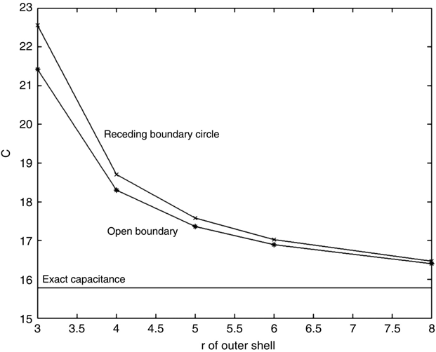
FIGURE 15.20 Results of open boundary condition approximation.
Another approach to dealing with the open boundary problem is exemplified by the gmsh file struct15_5.geo.
-
File
gmsh struct15_5.geo—layered resolution boundary region example:// structure file struct15_5.geo // 2nd program for setting up semi-infinite boundaries lc1 = 1.; lc2 = 1.5; lc3 = 2; Point(1) = {0, 0, 0, lc1}; // Center of structure high res Point(2) = {0, 0, 0, lc2}; // Center of structure low res Point(5) = {0,0,0, lc3}; // center of structure very low res sep = 3.; // Center - Center separation of inner circles Point(3) = {0, sep/2, 0, lc1}; Point(4) = {0, -sep/2, 0, lc1}; // 3rd level outer r3 = 6; Point(50) = {r3, 0, 0, lc3}; Point(51) = {0, r3, 0, lc3}; Point(52) = {-r3, 0, 0, lc3}; Point(53) = {0, -r3, 0, lc3}; Circle(54) = {50, 2, 51}; Circle(55) = {51, 2, 52}; Circle(56) = {52, 2, 53}; Circle(57) = {53, 2, 50}; Line Loop(58) = {54, 55, 56, 57}; // 2nd level outer r2 = 4; Point(10) = {r2, 0, 0, lc2}; Point(11) = {0, r2, 0, lc2}; Point(12) = {-r2, 0, 0, lc2}; Point(13) = {0, -r2, 0, lc2}; Circle(14) = {10, 2, 11}; Circle(15) = {11, 2, 12}; Circle(16) = {12, 2, 13}; Circle(17) = {13, 2, 10}; Line Loop(18) = {14, 15, 16, 17}; // Original Structure outer level r1 = 3; Point(20) = {r1, 0, 0, lc1}; Point(21) = {0, r1, 0, lc1}; Point(22) = {-r1, 0, 0, lc1}; Point(23) = {0, -r1, 0, lc1}; Circle(24) = {20, 1, 21}; Circle(25) = {21, 1, 22}; Circle(26) = {22, 1, 23}; Circle(27) = {23, 1, 20}; Line Loop(28) = {24, 25, 26, 27}; // Upper inner circle r0 = 0.5; Point(30) = {r0, sep/2, 0, lc1}; Point(31) = {0, r0 + sep/2, 0, lc1}; Point(32) = {-r0, sep/2, 0, lc1}; Point(33) = {0, sep/2-r0, 0, lc1}; Circle(34) = {30, 3, 31}; Circle(35) = {31, 3, 32}; Circle(36) = {32, 3, 33}; Circle(37) = {33, 3, 30}; Line Loop(38) = {34, 35, 36, 37}; // Lower inner circle r0 = 0.5; Point(40) = {r0, -sep/2, 0, lc1}; Point(41) = {0, r0-sep/2, 0, lc1}; Point(42) = {-r0, -sep/2, 0, lc1}; Point(43) = {0, -sep/2-r0, 0, lc1}; Circle(44) = {40, 4, 41}; Circle(45) = {41, 4, 42}; Circle(46) = {42, 4, 43}; Circle(47) = {43, 4, 40}; Line Loop(48) = {44, 45, 46, 47}; Plane Surface(100) = {28, 38, 48}; Plane Surface (19) = {18, 28}; Plane Surface (59) = {58, 18};
Program struct15_5.geo is a repeat of struct10.geo using a v = 0 outer boundary, but the space inside the outer boundary consists of successive annular rings, with the resolution decreasing (lc value increasing) as the radii of the rings increases. In other words, use less resolution where less resolution is needed. This example, with an outer radius of 6, results in a capacitance calculation of 17.33 pF/m. This is not quite as accurate as the capacitance predicted for an outer radius of 6 with uniform high resolution, but it is accomplished using significantly fewer nodes (169 vs. 321—almost a factor of 2 improvement). These results may, of course, be extended using larger outer rings and further decreased resolution. The attractive features of this approach are that there are no further mathematical approximations or program modifications necessary and that gmsh quite easily handles all of the details.
15.6 Dielectric Materials
It is very easy to modify the calculations and computer programs to correctly handle the effects of different dielectric constants in the structure, as long as the dielectric constant is uniform in each triangle. This isn't a limitation — simply define the triangles so that this condition is satisfied.
Going back to the derivations in Chapter 13, the total energy in the system is
The sum here is over all of the triangles in the structure.
In equation 15.16, the contribution from each triangle to U contains ε, the dielectric permittivity. Assume now that each triangle has a unique permittivity, ε= kT ε0, where kT is the relative dielectric constant of triangle T.
We build the coefficient matrix row by row by taking the derivative of equation (15.16) with respect to each node voltage and set this derivative to zero. When we do this, ε0/2 drops out but kT remains for each triangle’s (T) contribution.
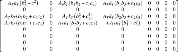
From a programming perspective, we must add the relative dielectric constant information to the structure’s description — either as a new column in the triangle’s data file or possibly as a new file altogether. Repeating the earlier example of triangle T’s contribution to the coefficient matrix, assume that we have an eight-triangle system with triangle T’s vertices at nodes 1, 3, and 4. The contribution to the coefficient matrix of triangle T is now equal to (see equation 13.13 for comparison)
Updating the earlier calculation is easy; when creating each triangle’s contribution to the coefficient matrix, simply multiply that triangle’s area by its (relative) dielectric constant.
As an example, consider the gmsh file struct15_6.geo—structure file for microstrip line example:
//  structure file struct15_6.geo
//  structure for symmetry calculation
//  stripline / microstrip line example

lc = .2;     // background resolution

t = .1;      // thickness of center conductor
w = 1.0;     // 1/2 width of center conductor
h = 8;      // height of box
d = 2.;      // height of dielectric slab
b = 4;      // 1/2 width of outer box

Point(1) = {0, 0, 0, lc};
Point(2) = {b, 0, 0, lc};
Point(3) = {b, h, 0, lc};
Point(4) = {0, h, 0, lc};
Point(5) = {0, d + t, 0, lc};
Point(6) = {w, d + t, 0, lc/5}; // higher resolution near the conductor edges
Point(7) = {w, d, 0, lc/5};
Point(8) = {0, d, 0, lc};

Line(1) = {1, 2};
Line(2) = {2, 3};
Line(3) = {3, 4};
Line(4) = {4, 5};
Line(5) = {5, 6};
Line(6) = {6, 7};
Line(7) = {7, 8};
Line(8) = {8, 1};
Line Loop(1) = {1, 2, 3, 4, 5, 6, 7, 8};
Plane Surface(1) = {1} ;
File struct15_6.geo utilizes X symmetry and creates a boxed microstrip cross section. It is set up with a relatively low-resolution meshing, except in the area of the edge of the center conductor. The resulting mesh file may be parsed through parse_msh_file2.m and then the FEM analysis performed using fem_2d.m.
The purpose of this example is to create a dielectric slab in the region below the center conductor (y = d = 2.0 in the struct15_6.geo file) and modify fem_2d.m to correctly set up and solve the FEM model.
Our first task arises, as may be seen by examining the mesh file Figure 15.22a is to create a straight edge along y = d so that the dielectric slab region can be defined (Figure 15.22b). Since struct15_6.geo was created without this goal in mind, the resulting mesh triangle vertices are not along the desired interface line.
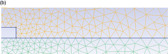
FIGURE 15.22 gmsh structure file with dielectric slab edge defined.
This issue is resolved in struct15_7.geo—struct15_6 with dielectric edge delineated—by adding a line along what will be the dielectric surface:
// structure file struct15_7.geo
// structure for symmetry calculation
// stripline / microstrip line example
// dielectric edge line added

 lc = .2; // background resolution

 t = .1; // thickness of center conductor
 w = 1.0; // 1/2 width of center conductor
 h = 8; // height of box
 d = 2.; // height of dielectric slab
 b = 4; // 1/2 width of outer box

 Point(1) = {0, 0, 0, lc};
 Point(2) = {b, 0, 0, lc};
 Point(3) = {b, h, 0, lc};
 Point(4) = {0, h, 0, lc};
 Point(5) = {0, d + t, 0, lc};
 Point(6) = {w, d + t, 0, lc/5}; // higher resolution near the conductor edges
 Point(7) = {w, d, 0, lc/5};
 Point(8) = {0, d, 0, lc};
 Point(9) = {b, d, 0, lc};

 Line(1) = {1, 2};
 Line(2) = {2, 9};
 Line(3) = {9, 7};
 Line(4) = {7, 8};
 Line(5) = {8, 1};

// Lower box
 Line Loop(1) = {1, 2, 3, 4, 5};
 Plane Surface(1) = {1} ;

 Line(6) = {9, 3};
 Line(7) = {3, 4};
 Line(8) = {4, 5};
 Line(9) = {5, 6};
 Line(10) = {6, 7};

//upper box
 Line Loop(2) = {-3, 6, 7, 8, 9, 10};
 Plane Surface(2) = 2;
Two modifications to fed_2d.m are required in order to perform the dielectric edge calculation, and then a modification to the capacitance calculation function:
- MATLAB program
fem_2d_diel.m—namely,fem_2d_2.mwith dielectric region capability:% 2d FEM with triangles % fem_2d_4.m is an extension of fem_2d_2.m, with dielectric regions close clear filename = input('Generic name for input files: ', 's'), nodes_file_name = strcat('nodes_', filename, '.txt'), trs_file_name = strcat('trs_', filename, '.txt'), bcs_file_name = strcat('bcs_', filename, '.txt'), % get node data from file nds = get_nodes(nodes_file_name); nr_nodes = length(nds.x) % get triangles data from file trs = get_triangles(trs_file_name); nr_trs = length(trs) % get bcs data from file bcs = get_bcs(bcs_file_name); nr_bcs = length(bcs.node) edge_y = 2.0; % allocate the matrices a = sparse(nr_nodes, nr_nodes); f = zeros(nr_nodes,1); b = zeros(3,nr_nodes); c = zeros(3,nr_nodes); % generate the matrix terms d = ones(3,3); all_er = []; for tri = 1: nr_trs % Walk through all the triangles n1 = trs(1,tri); n2 = trs(2,tri); n3 = trs(3,tri); d(1,2) = nds.x(n1); d(1,3) = nds.y(n1); d(2,2) = nds.x(n2); d(2,3) = nds.y(n2); d(3,2) = nds.x(n3); d(3,3) = nds.y(n3); Area = det(d)/2; % ---- Patch for dielectric region th = 1.001*edge_y; % Height of the dielectric layer er = 20; % Dielectric constant if nds.y(n1) < = th & nds.y(n2) < = th & nds.y(n3) < = th Area = Area*er; all_er = [all_er, er]; else all_er = [all_er, 1]; end % ------------------------------------------------------- temp = d[1; 0; 0]; b(1,tri) = temp(2); c(1,tri) = temp(3); temp = d[0; 1; 0]; b(2,tri) = temp(2); c(2,tri) = temp(3); temp = d[0; 0; 1]; b(3,tri) = temp(2); c(3,tri) = temp(3); a(n1,n1) = a(n1,n1) + Area*(b(1,tri)^2 + c(1,tri)^2); a(n1,n2) = a(n1,n2) + Area*(b(1,tri)*b(2,tri) + c(1,tri)*c(2,tri)); a(n1,n3) = a(n1,n3) + Area*(b(1,tri)*b(3,tri) + c(1,tri)*c(3,tri)); a(n2,n2) = a(n2,n2) + Area*(b(2,tri)^2 + c(2,tri)^2); a(n2,n1) = a(n2,n1) + Area*(b(2,tri)*b(1,tri) + c(2,tri)*c(1,tri)); a(n2,n3) = a(n2,n3) + Area*(b(2,tri)*b(3,tri) + c(2,tri)*c(3,tri)); a(n3,n3) = a(n3,n3) + Area*(b(3,tri)^2 + c(3,tri)^2); a(n3,n1) = a(n3,n1) + Area*(b(3,tri)*b(1,tri) + c(3,tri)*c(1,tri)); a(n3,n2) = a(n3,n2) + Area*(b(3,tri)*b(2,tri) + c(3,tri)*c(2,tri)); end %bcs for i = 1: nr_bcs if bcs.volts(i) > = 0 n = bcs.node(i); a(n,:) = 0; a(n,n) = 1; f(n) = bcs.volts(i); end end % fake bcs for nodes in excluded region - assuming boundary at 1 volt % There might not be any excluded regions in symmetry problems % This is being left for backwards-compatibility of the program for i = 1 : nr_nodes if a(i,i) == 0 a(i,:) = 0; a(i,i) = 1; f(i) = 1; end end v = af; % plot the mesh show_mesh2(nr_nodes, nr_trs, nr_bcs, nds, trs, bcs, v) % calculate capacitance C = get_tri2d_cap_diel(v, nr_nodes, nr_trs, nds, trs, all_er) % show field profile get_tri2d_E(v, nr_nodes, nr_trs, nds, trs) % show voltage along y = 0 edge_y x_temp = []; v_temp = []; for i = 1 : nr_nodes if nds.y(i) == 0 % fprintf ('%d %d %f ', i, nds.y(i), v(i)) x_temp = [x_temp, nds.x(i)]; v_temp = [v_temp, v(i)]; end end figure(4) plot(x_temp, v_temp, '.') -
MATLAB program
get_tri2d_2d_cap_diel.m—capacitance calculation with dielectric region capability:function C = get_tri2d_cap_diel(v, nr_nodes, nr_trs, nds, trs, all_er) % Calculate the capacitance of a 2d triangular structure % dielectric region added eps0 = 8.854; U = 0; d = ones(3,3); for tri = 1 : nr_trs n1 = trs(1,tri); n2 = trs(2,tri); n3 = trs(3,tri); d(1,2) = nds.x(n1); d(1,3) = nds.y(n1); d(2,2) = nds.x(n2); d(2,3) = nds.y(n2); d(3,2) = nds.x(n3); d(3,3) = nds.y(n3); temp = (d[1; 0; 0]); b1 = temp(2); c1 = temp(3); temp = (d[0; 1; 0]); b2 = temp(2); c2 = temp(3); temp = (d[0; 0; 1]); b3 = temp(2); c3 = temp(3); Area = det(d)/2; if Area < = 0, disp 'Area < = 0 error'; end; U = U + all_er(tri)*Area*((v(n1)*b1 + v(n2)*b2 + v(n3)*b3)^2 ⋯ + (v(n1)*c1 + v(n2)*c2 + v(n3)*c3)^2); end U = U*eps0/2; C = 2*U; % Potential difference of 1 volt assumed end
In the FEM analysis, the dielectric region is defined and each triangle’s area is multiplied by the (relative) dielectric constant as needed. An array all_er is created for convenience in passing the dielectric region information to the capacitance calculated.
In parse_msh_file2.m, the -9999 boundary condition entry was created to specify a symmetry edge. In struct15_6.geo and struct15_7.geo this capability is used on the two left edge lines. Program fem_2d.m translates this boundary condition into the required “do nothing” for nodes along the symmetry line. In struct15_7.geo, the interface line between the dielectric and air regions shows up as a line requiring a boundary condition. Specifying -9999 for this line produces the desired result. Each time the program encounters these nodes in setting up the boundary conditions, it treats these nodes as if they were internal nodes; these nodes show up for every triangle using these nodes, on both sides of the dielectric interface, resulting in the correct coefficient matrix assembly.
The full boundary condition specification information is listed here:
| Line N Number | Boundary Condition |
| 1 | 0 (default) |
| 2 | 0 (default) |
| 3 | -9999 |
| 4 | 1 |
| 5 | -9999 |
| 6 | 0 (default) |
| 7 | 0 (default) |
| 8 | -9999 |
| 9 | 1 |
| 10 | 1 |
The following table lists the results of this capacitance calculation as compared to published results for open microstripline:7
| Relative Dielectric Constant | FEM Analysis | Published Results | Error (%) |
| 1 | 30.6 | 27.4 | 12.0 |
| 2 | 47.6 | 44.5 | 7.0 |
| 10 | 182.8 | 177.0 | 3.3 |
| 20 | 351.0 | 342.1 | 2.6 |
The results are relatively poor for a relative dielectric constant of one (12%); the calculated capacitance is much too high, but improves as the dielectric constant increases. The extra capacitance can be attributed to the finite distance to the sidewall and topwall in the FEM calculation; the published results pertain to an open line (with no sidewall or topwall). As the dielectric constant increases (not changing the resolution, i.e. using the same struct15_7.msh file), the fraction of electric field energy stored in the dielectric increases and the presence of the sidewall and topwall become less and less significant.
This program, as written, is awkward. Two straightforward improvements would be to
- Create a new file for the boundary condition specification: This would save a tedious and error-prone user input process.
- Create a file containing the dielectric constant information or augment the triangle information file with this information. Operationally, both approaches are equivalent; however, the former approach can be written to maintain compatibility with earlier data files by having the program default the entire mesh to an air dielectric if no dielectric constant file is found.
Problems
- 15.1 Write a simple
gmshfile for a circular coaxial cable cross section with inner radius 1 and outer radius 2. Start with the inner circle centered inside the outer circle (a concentric cable) and then move the inner circle in small increments in any direction toward an outer wall. Plot how the capacitance and the peak electric field magnitude vary with the position of the center conductor. - 15.2 Referring to the structure of Problem 15.1, return the inner circle to the center and then modify the
.geofile to allow subsections to be drawn as shown in Figure P15.2. The capacitance, voltage, and electric field distributions of the full line may then be found by considering the two (straight) radial lines, symmetry axes. Calculate the capacitance and the peak electric field of the full structure for several values of the angle φ shown in Figure P15.2.
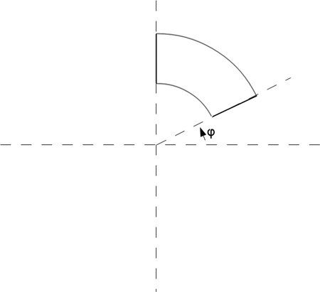
FIGURE P15.2 Sample subsection of concentric coaxial line.
- 15.3 For values of φ approaching 90°, Figure P15.2 resembles the cross section of a parallel plate capacitor that is infinite in extent and is being modeled using symmetry axes. Can an approximate capacitance expression for the concentric coaxial cable be derived using only the ideal parallel plate capacitor equation?
- 15.4 A finite length of transmission line will have a series of resonance frequencies, that is, frequencies at which the line will support standing waves. This is directly analogous to the audiofrequencies produced by a violin string. (One of) these frequencies may be used, with supporting electronics, to create a frequency reference signal. Suppose that we wish to use a boxed microstrip line. Assume the line to be infinite in extent for a capacitance calculation, and ignore the fringing capacitances discussed in the MoM chapters. The resonance frequency of the line will vary, to a good approximation, with
 , where C is the center conductor to outer box capacitance. Unfortunately, the top of the outer box, which is a sheet of metal supported only at its edges, is easily flexed by outside forces (e.g., stresses due to mounting the microstrip package in a product of some sort), and even with identical microstip packages, the resulting resonance frequency is too unpredictable for practical use.
- For the dimensions shown, calculate the relative variation in resonance frequency due to the box cover flexing. Approximate the flexing as a small change in overall box height.
- Double the relative dielectric constant of the dielectric slab (from 10 to 20). Reduce the center conductor width to get the capacitance back to its original value. Now repeat part a. Have we made things better or worse? Here is the
gmshstructure file for Problem 15.4:
// structP15_4.geo This is the same structure as struct51.geo,
// the dimensions have been changed

lc = .2; // background resolution

t = .025; // thickness of center conductor
w = .070; // 1/2 width of center conductor
h = 1.98; // height of box
d = 1.; // height of dielectric slab
b = 2.500; // 1/2 width of outer box

Point(1) = {0, 0, 0, lc};
Point(2) = {b, 0, 0, lc};
Point(3) = {b, h, 0, lc};
Point(4) = {0, h, 0, lc};
Point(5) = {0, d + t, 0, lc};
Point(6) = {w, d + t, 0, lc/5}; // higher resolution near the conductor edges
Point(7) = {w, d, 0, lc/5};
Point(8) = {0, d, 0, lc};
Point(9) = {b, d, 0, lc};

Line(1) = {1, 2};
Line(2) = {2, 9};
Line(3) = {9, 7};
Line(4) = {7, 8};
Line(5) = {8, 1};

// Lower box
Line Loop(1) = {1, 2, 3, 4, 5};
Plane Surface(1) = {1} ;

Line(6) = {9, 3};
Line(7) = {3, 4};
Line(8) = {4, 5};
Line(9) = {5, 6};
Line(10) = {6, 7};

//upper box
Line Loop(2) = {-3, 6, 7, 8, 9, 10};
Plane Surface(2) = 2;
References
- 1. Y. Kwon and H. Bang, The Finite Element Method Using Matlab, 2nd ed., CRC Press, Boca Raton, FL, 2000.
- 2.
http://galileoandeinstein.physics.virginia.edu/142E/10_1425_web_ppt_pdfs/10_1425_web_Lec_17_CenterOfMassEtc.pdf. - 3.
http://www.heisingart.com/dvc/ch%2009%20center%20of%20mass.pdf. - 4.
http://faculty.trinityvalleyschool.org/hoseltom/handouts/Center%20of%20Mass3.pdf. - 5. W. R. Smythe, Static and Dynamic Electricity, Section 4.14, McGraw Hill, New York, 1950.
- 6. M. V. K. Chari and S. J. Salon, Numerical Methods in Electromagnetism, Academic Press, San Diego, 2000.
- 7.
http://www.cepd.com/calculators/microstrip.htm.