
Chapter 2
Computer Organization and Hardware
This chapter examines the hardware of a computer: the central processing unit (CPU), memory, the I/O subsystem, and the bus. Each of these components is described in detail to provide an understanding of its role. In examining the CPU, the chapter emphasizes the fetch–execute cycle. An example program is used to illustrate the fetch–execute cycle. The CPU’s components are themselves examined: the control unit, the arithmetic logic unit, and registers. In examining memory, the memory hierarchy is introduced and the different forms of memory are discussed: RAM, SRAM, DRAM, ROM, virtual memory. In the discussion of input and output devices, topics of human–computer interaction (HCI) and ergonomics are emphasized. The chapter includes a discussion on how to assemble the various computer components. The intent of this chapter is to provide the IT student with a solid foundation in computer hardware.
The learning objectives of this chapter are to
- Identify the components of a computer and their roles.
- Describe the fetch–execute cycle.
- Discuss characteristics that impact a processor’s performance.
- Describe the different levels of the memory hierarchy.
- Describe the role of the various types of input and output devices.
- Discuss the impact that I/O devices have on the human body and the importance of HCI.
- Illustrate how a computer can be assembled from component parts.
Computer organization is the study of the components of a computer, their function, their structure (how they work), and how they are connected together. This topic is common in computer science programs as a sophomore or junior level class. Here, while we will look at these components, we will look more at their function and how they are connected together. By studying computing organization, you will gain an understanding of how computers work and the importance of each of the primary components, as introduced in Chapter 1. This chapter concludes with a section that discusses computer hardware and the process of assembling (building) a computer from component parts.
A computer consists of a central processing unit (CPU), memory and storage, and peripheral devices (including some form of network connection). A computer performs four operations:
- Input
- Processing
- Output
- Storage
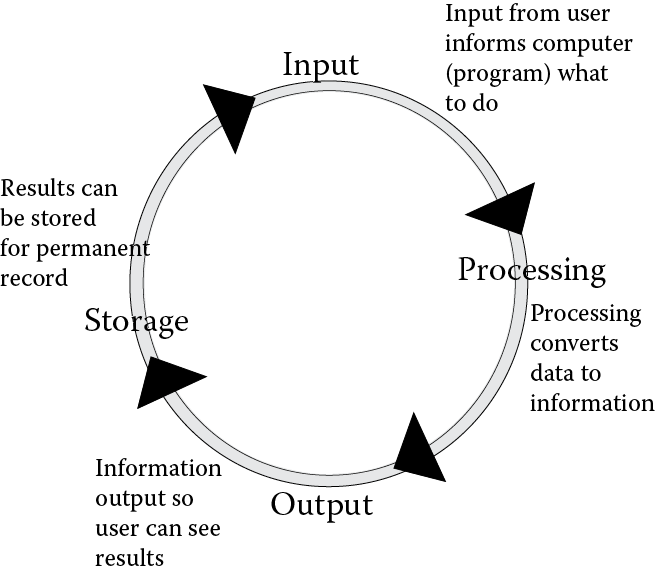
The IPOS cycle—input–processing–output–storage—describes roughly how we use a computer. We input data, process it, output the results, and store any information that we want to keep permanently. Figure 2.1 illustrates the IPOS cycle. Describing the computer at this level does not really tell us what is going on—for instance, how does storage differ from memory, and how does the processing take place? So we will take a closer look here.
Structure of a Computer
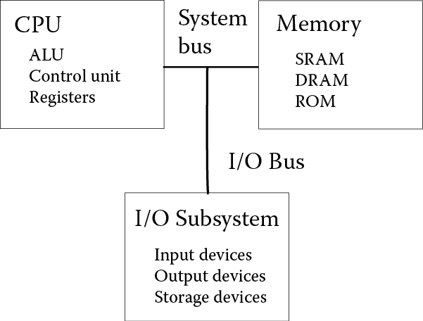
Figure 2.2 shows the overall structure of most computer systems. As you can see, there are four components: the CPU (or processor), memory, input/output (I/O) subsystem, and the bus. The CPU is the device that not only executes your programs’ instructions, but also commands the various components in the computer. Memory stores the program(s) being executed and the data that each program is using. The I/O subsystem includes all peripheral devices (input, output, storage, network) where storage consists of the long-term storage devices (disk drives, tape). The bus is the device that permits information to move between each component.
Before we continue with our look at the computer’s components, we have to understand that the devices in the computer are digital devices. Inside the computer, digital data are represented as electrical current being in one of two states: high or low. High means that there is a noticeable current flowing through the component, and low means that there is no, or nearly no, current flowing. We will assign the number 1 to be high current and 0 to be low (or no) current. The bus then is perhaps an easy device to understand. The bus consists of a number of wires, each wire allows 1 bit (a single 1 or 0, high or low current) to flow over it. We discussed storage capacity previously in Chapter 1 (see Table 1.4) but for now, we will define three terms: a bit (a single 1 or 0), a byte (8 bits, using eight wires on the bus, usually the smallest unit of data transfer), and a word (today, computers have either 32-bit or 64-bit words; the word size is the typical size of a datum).
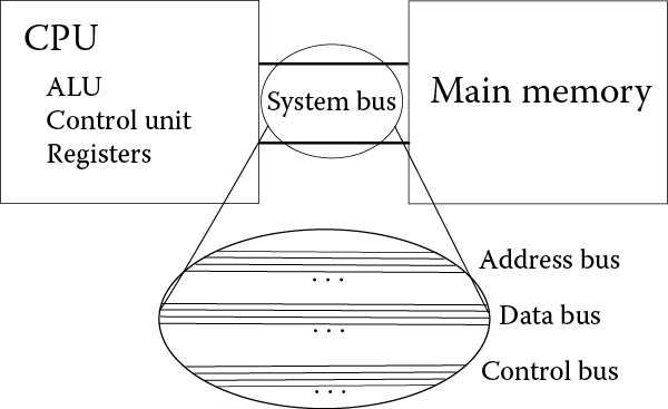
The bus actually consists of three parts: the address bus, the control bus, and the data bus. These three parts of the bus perform the following operations:
- The address bus is used by the CPU to send addresses to either memory or the I/O subsystem. An address is the location that the CPU either wants to retrieve a datum from, or the location that the CPU wants to store a datum to. The CPU more commonly addresses memory than I/O. Note that a datum might either be a value to be used in a program, or a program instruction.
- The control bus is used by the CPU to send out commands. Commands might be “read” or “write” to memory, or “input”, “output”, or “are you available” to an I/O device. The control bus is also used by the various devices in the computer to send signals back to the CPU. The primary signal is known as an interrupt, which is a request by a device (e.g., disk drive, printer) to interrupt the CPU and ask for its attention.
- The data bus is used to send data (including program instructions) from memory to the CPU, or data from the CPU to memory, or between I/O devices and the CPU or memory.
The size of the data bus is typically the size of the computer’s word. The size of address bus is based on the size of addressable memory. The size of the control bus is based on the number of different commands that the CPU might send out. See Figure 2.3, where the data bus would probably be 32 bits in size, and the address and control bus size would depend on a number of different issues. The bus shown in this figure is the system bus. Another bus, the local bus, connects the components of the CPU [ALU (arithmetic/logic unit), control unit, registers] and yet another bus connects the I/O devices together.
What Are Pins?
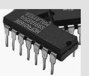
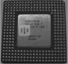
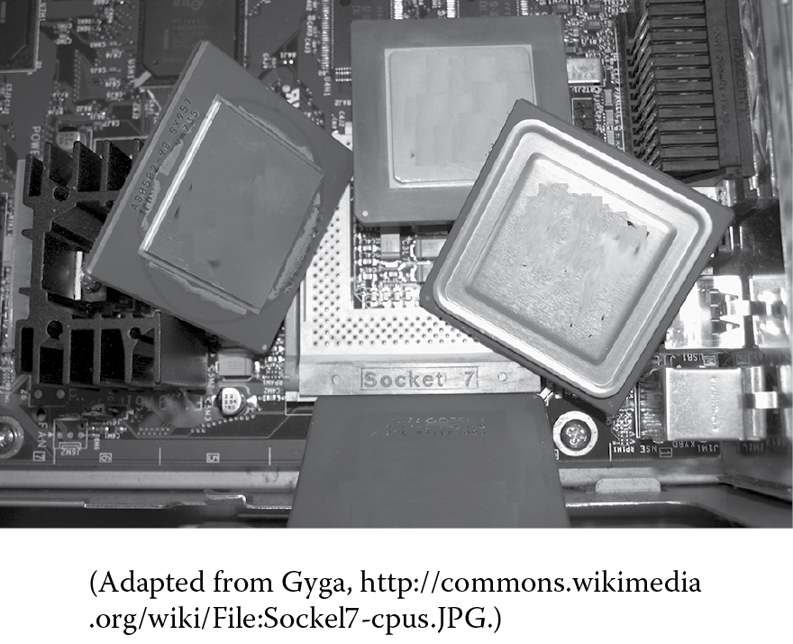
Take a look at a CPU. You will see a number of metal pins that come out of the bottom. The pins are used to connect the CPU into a socket. The socket connects to the system bus. Therefore, each pin connects to one line of the bus. Earlier CPUs had few pins, whereas today CPUs can have more than a thousand pins! Thus, pins have to be very small to fit. Also, every pin requires a certain amount of power so that current could potentially flow over any or all pins at any time. So our modern CPUs require greater power consumption. This, in turn, gives off more heat, so we need more powerful cooling of the CPU. Below are two Intel CPUs, an early CPU from the 1970s with just a few dozen pins, and a modern Pentium processor with almost 500 pins.
(Adapted from Kimmo Palossaari, http://commons.wikimedia.org/wiki/File:IC_DIP_chips.JPG, and Stonda, http://commons.wikimedia.org/wiki/File:Pentium-60-back.jpg.)
A Program
In order to understand the CPU, we have to understand a computer program. This is because the CPU executes programs. So, we will first examine a simple program. The following program is written in C although it could be written in nearly any language. The only thing that would change is the syntax. The // marks indicate comments. Comments will help you understand the program.
#include <stdio.h> //input/output library
void main() //start of the program
{
int a, b, c; //use 3 integer variables
scanf(“%d”, &a); //input a
scanf(“%d”, &b); //input b
if(a < b) //compare a to b, if a is less then b
c = a + b; //then set c to be their sum
else c = a-b; //otherwise set c to be their difference
printf(“%d”, c); //output the result, c
}
This program inputs two integer values from the user, and if the first is less than the second, it computes c = a + b (c is the sum of the two) otherwise, it computes c = a – b (c is a minus b). It then outputs c. If, for instance, the user inputs 5 and 10, it computes c = 15 and outputs 15. If instead the user inputs 5 and 3, it computes c = 2 and outputs 2. This is a fairly pointless program, but it will serve for our example.
Once written, what happens to the C program? Can I run this program? No. No computer understands the C programming language. Instead, I have to run a special program called a compiler. The compiler translates a program into a simpler language called machine language. The machine language version of the program can then be executed. Machine language is archaic and very difficult to read, so we will look at an intermediate form of the program, the assembly language version. Again, comments will occur after // marks.
Input 33 //assume 33 is the keyboard, input a value
//from keyboard
Store a //and store the value in the variable a
Input 33 //repeat the input for b
Store b
Load a //move a from memory to CPU, a location
//called the accumulator
Subt b //subtract b from the accumulator
//(accumulator = a – b)
Jge else //if the result is greater than or equal
//to 0, go to location “else”
Load a //otherwise, here we do the then clause,
//load a into accumulator
Add b //add b (accumulator is now a + b)
Store c //store the result (a + b) in c
Jump next //go to the location called next
else: Load a //here is the else clause, load a into the
//accumulator
Subt b //subtract b (accumulator is now a – b)
Store c //store the result (a – b) into c
next: Load c //load c into the accumulator
Output 2049 //send the accumulator value to the output
//device 2049, assume this is the monitor
Halt //end the program
The assembly language version of the program consists of more primitive instructions than the C version. For instance, the single scanf statement in C, which can actually be used to input multiple values at a time, is broken into input and store pairs for each input. The C if statement is broken into numerous lesser statements. Now, recall that an assembly language program is supposed to be simpler than a high level language program. It is simpler in that each assembly language instruction essentially does one primitive thing. However, for our programs to accomplish anything useful, we need far more assembly language instructions than high level language instructions. You might think of the two types of languages in this way: an assembly language instruction is like the nuts and bolts of construction, whereas the high level language instruction is like prefabricated components such as hinges and locks. The computer cannot do something like scanf, or an if–else statement directly in one instruction, but it can do a load, add, store, or jump in single operations.
As with the C program, a computer cannot execute an assembly language program either. So, our program must next be converted from assembly language into machine language. The reason why we showed the assembly language program is that it is easier to understand than a machine language program.
A compiler is a program that translates a source program written in a high-level language, such as C, into machine language. An assembler is a program that translates an assembly language program into machine language. So imagine that we have translated the previous assembly program into machine language. A portion of the final program might look something like this:
1000100 0000000000000000000100001 —input (from keyboard)
1000111 0010011000100101101010001 —store the datum in a
1000100 0000000000000000000100001 —input (from keyboard)
1000111 0010011000100101101010010 —store the datum in b
The remainder of the machine language program is omitted because it would make no more sense than the above listing of 1s and 0s. If you look at the 1s and 0s, or binary numbers, you might notice that they are formatted into two parts. These two parts represent each instruction’s operation (the first 7 bits) and the operand, or datum. Here, the operation denotes one of perhaps 100 different instructions. 1000100 represents “input” and 1000111 represents “store”. There would similarly be operations for “add”, “subt”, “jge”, “load”, and “jump”. The operand denotes a memory location written in binary (for instance, datum a is stored at location 0010011000100101101010001, which is address 5,000,017, and the value 0000000000000000000100001 denotes a device number, 33, for the keyboard). Although this machine language code is made up for the example, it is not too different from what we might find if we studied specific machine languages.
Executing the Program
Okay, back to computer organization. We want to run this simple program. The first thing that happens when you want to run a program is that the operating system loads the program from where it is stored on the hard disk into a free section of memory. We will assume that the operating system has placed it at memory location 5,000,000. Because there are 17 instructions, the program will be stored consecutively from memory location 5,000,000 to 5,000,016. We will also assume that the variables, a, b, and c, are stored immediately after the program, in memory locations 5,000,017 through 5,000,019, respectively, for a, b, and c. Once loaded, the operating system transfers control to the processor (CPU) to begin running this program.
Now we have to understand in more detail what the CPU and memory do. The CPU consists of the control unit, the ALU, and registers. One of those registers is called the program counter, or PC (not to be confused with the generic name of a home computer). The PC gets the address of the first program instruction in memory, 5,000,000. Another register is called the instruction register (IR). It stores the current instruction. Another register is called the status flags (SFs); it stores the result of the most recent ALU computation in terms of whether the result was positive, negative, zero, caused an overflow, caused an interrupt, had a value of even parity, and so forth. Each of these items is stored in 1 bit, so the SF will store multiple results, although most of the bits will be 0. Other registers are data registers—they store data that we are currently using. One special data register, called the accumulator (AC), is used for storing the most recent value computed or used.
We are ready to look at how the CPU runs the program. The CPU performs what is known as the fetch–execute cycle. The idea behind this cycle is that the CPU first fetches an instruction from memory, and then executes it. In fact, there is more to it than that. The typical fetch–execute cycle (the cycle differs depending on the processor) will have four or five, or maybe more, stages (Figure 2.4).
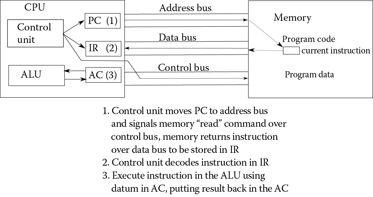
For our example, we will assume a five-part cycle* with the following stages:
- Fetch instruction from memory.
- Decode the instruction from machine language into microcode.
- Fetch the operands from registers.
- Execute the instruction.
- Store the result back into a register.
In Figure 2.4, steps 3–5 are all indicated as step 3, executing the instruction using the data register. However, in many CPUs, there are several, even dozens of registers. This requires that steps 3 and 5 be separated from step 4.
Step 4 from our five-part cycle is where the instruction is executed. However, as you see, this is not the only step required to execute an assembly language operations. Without all of the stages, the program does not run correctly. Microcode, mentioned in step 2, will be discussed later in the chapter.
So let us see how the program discussed in the last section will be executed on this five-part cycle. The first thing that happens is that the CPU fetches the first program instruction. This occurs by sending the value stored in the PC (the memory location of the first instruction) to memory over the address bus, and sending a “read” signal over the control bus. Memory receives both the address and the “read” command, and performs the read access at the given memory location. Whatever it finds is then sent back to the CPU over the data bus. In this case, what is sent back to the CPU is not a datum but a program instruction, and in the case of our program, it is the instruction “Input”, written in binary as:
1000100 0000000000000000000100001
Once the instruction is received by the CPU, it is stored in the IR. To end this stage, the CPU increments the PC to 5,000,001 so that it now indicates the location of the next instruction to be fetched.
The next stage is to decode the instruction. The control unit breaks the instruction into two or more parts—the operation (in this case, the first 7 bits) and the operand(s). In essence, the control unit consults a table of operations to find 1000100, the instruction “Input”. This informs the CPU that to execute the instruction, it needs to perform an input operation from the input device given by the address in the operand. The operand is the binary number for 33, which (in our fictitious computer) is the keyboard.
As there are no operands to fetch, stage 3 is skipped. Stage 4 is the execution of the instruction. The input instruction requires that the CPU communicate with the input device (the keyboard) and retrieve the next datum entered. The execution of the input instruction is not typical in that the CPU does not proceed until the user has entered something. At that point, the CPU retrieves the datum over the data bus and brings it into the CPU. The fifth and final stage requires moving the value from the data bus into the AC register.
We have now seen the full execution of our program’s first instruction. What happens next? The entire fetch–execute cycle repeats. In fact, it will continue repeating until the program terminates.
For the second instruction, the first step is to fetch the instruction from memory. Now, the PC has the address 5,000,001, so the CPU fetches the instruction at that location from memory. The PC value is placed on the address bus, the control unit signals a memory read across the control bus, memory looks up that address and returns the contents over the data bus, and the item is stored in the IR. The last step of the fetch phase is to increment the PC to now point at 5,000,002. The instruction in the IR is
1000111 0010011000100101101010001
which is “store a”.
The decode stage determines that the operation is a store operation, which requires moving a datum from the AC into main memory. The address that will receive the datum from the AC is stored as the second portion of the instruction, 5,000,017 (the address of a).
To execute the instruction, the latter part of the IR is moved to the address bus, the value in the AC is moved to the data bus, and the control unit signals a memory “write” over the control bus. The execution of the instruction is now in the hands of main memory, which takes the value from the data bus and stores it at the memory location received over the address bus (5,000,017). This instruction does not require a fifth step as the CPU itself does not need to store anything.
The next two instructions occur in an almost identical manner except that these instructions are at 5,000,002 and 5,000,003, respectively, and the second datum is stored at memory location 5,000,018 (b). By the time these two instructions have been executed, the PC will be pointing at location 5,000,004, and memory locations 5,000,017 and 5,000,018 will store the first two input values, a and b, respectively.
The fifth instruction is fetched and stored in the IR. This instruction is “load a”. The execution of this instruction sends the address, 5,000,017, across the address bus and a memory read signal over the control bus. Memory looks up the datum stored at this location and sends it back over the data bus. The final stage of this instruction is to store the resulting datum in the AC. Notice that unlike the previous “memory read” operations discussed in this section, this is a memory read of a true datum, not of an instruction. Figure 2.5 illustrates the difference between the “load” (upper portion of the figure) and “store” (lower portion of the figure) instructions, that is, between a memory read and a memory write.
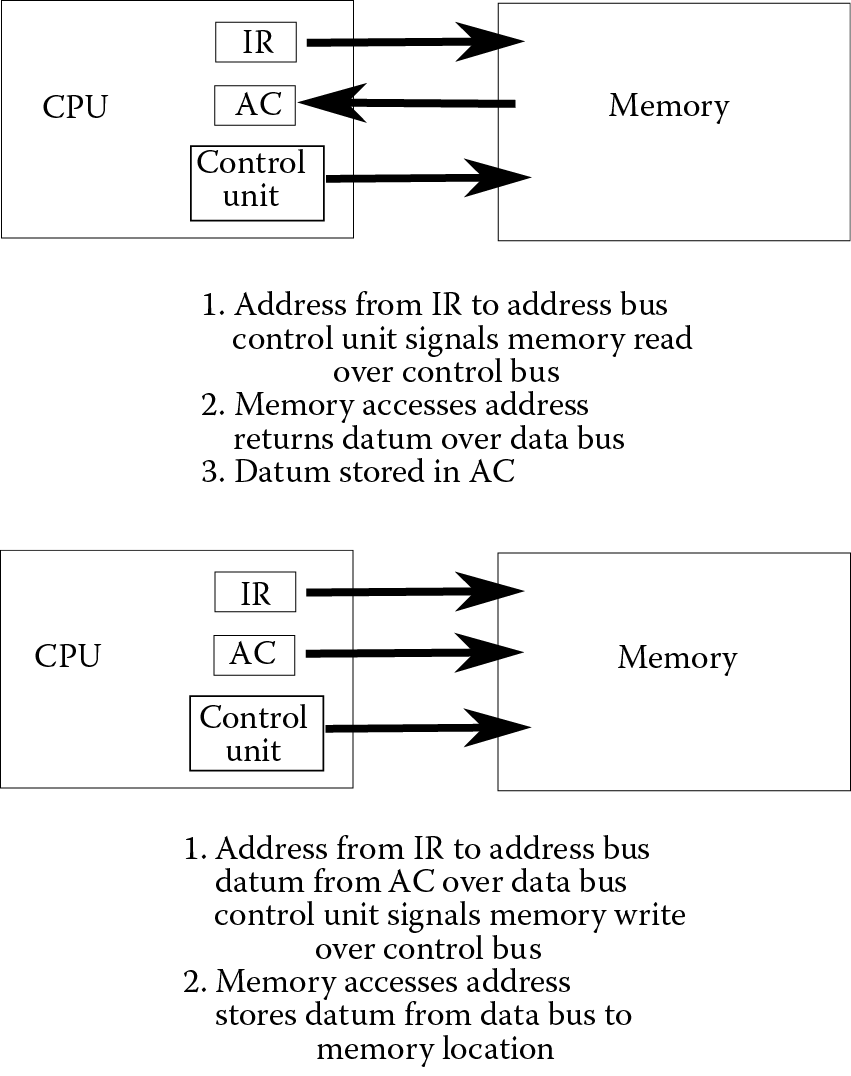
The sixth instruction, “subt b”, starts off similar to the fifth, “load a”. The instruction is fetched as before, with the “subt b” placed in the IR and the PC incremented. The control unit then decodes this instruction. However, the execution stage for subtraction differs from load because this instruction requires two separate execution steps. First, memory is read, similar to “load a” but in this case, the address is 5,000,018 (the variable b). The datum that is returned from memory is not stored in the AC though. Instead, the contents of the AC and the datum returned from memory are both sent to the ALU. The control unit signals the ALU to perform a subtraction. The subtraction circuit operates on the two data and the result, coming out of the ALU, is the value from the AC minus the value from memory (i.e., a – b). The store result step of this instruction is to take that result from the ALU and move it to the AC.
The ALU also sets a status flag based on the result of the subtraction. The SFs are used to indicate the results of ALU operations, such as whether the result was positive, zero, or negative, or whether the result caused an overflow or a carry out or an interrupt. The flags are usually denoted as PF (positive flag), ZF (zero flag), NF (negative flag), OF (overflow flag), and so forth. Any ALU operation will result in at least one flag being set (changing from 0 to 1). We will see how these flags are used in the next instruction.
The seventh instruction (at 5,000,006) is the first instruction that you might not understand by reading the assembly language code. It says “jge else”. This means “jump on greater than or equal to the location else”. The location “else” is another memory location. Because the first instruction in the program is at memory location 5,000,000, the “else” location is at 5,000,011 (it is the 12th instruction in the program). Refer back to the program in the last section. As with all previous instructions, this instruction (“jge else”) is fetched from memory into the IR and decoded. The execution stage works as follows:
If either the PF or ZF is set (the subtraction resulted in a positive or zero result), then reset the PC to the location of “else”. If the NF is set, then do nothing.
This means that, if the previous instruction (the subtraction) resulted in a positive or zero result, branch to location “else”. We use the PF and ZF here because the instruction specifies “greater than or equal to”. Had the instruction been “less than”, we would only use the NF. Other comparisons include “equal to”, “not equal to”, “greater than”, and “less than or equal to”. At the end of this instruction, the PC will either be 5,000,007 (the next sequential instruction) or 5,000,011 (the location of else).
The eighth instruction then depends on what happened in the seventh. Either the CPU fetches the instruction at 5,000,007 or 5,000,011. Whichever is the case, the next three instructions are nearly identical. They are to “load a”, “add/subt b”, and “store c”. That is, the group of three instructions either perform c = a + b or c = a – b depending on which of the two sets of code is executed. Assuming that we have executed the instructions starting at 5,000,007, then the instruction at 5,000,010 is “jump next”. This instruction will change the PC value to be 5,000,012 (the location of next). Whichever path led us here, the last three instructions are “load c”, “output”, “halt”. The output instruction takes whatever is in the AC and moves it to the output device listed (2049, presumably the monitor). When the CPU executes the “halt” instruction, the program ends and control reverts to the operating system.
Role of CPU
The CPU processes our programs. It does so using two different pieces of hardware. The first is the ALU, which executes all arithmetic and logic operations. The ALU has individual circuits for performing the various operations. An adder is used to perform both addition and subtraction. A multiplier is used for multiplication. A divider is used for division. A comparator is used to compare two values (for instance, to determine if a > b). Other circuits perform shifting, rotating, and parity computation (see Chapter 3).
The second piece of hardware is the control unit. The control unit is responsible for controlling (commanding) all of the components in the computer. As we saw in the example in Executing the Program, the control unit sends out such signals as a memory read or a memory write. It also sends signals to the ALU such as to perform a subtraction or a comparison. The control unit controls the fetch–execute cycle. First, it accomplishes the fetch stage. Then it decodes the fetched instruction into microcode. This, in turn, instructs the control unit on how to execute the instruction. Therefore, the control unit will have separate sets of commands for the instruction fetch stage, and for every machine instruction. Some instructions require an operand, and so the control unit handles how to acquire the operand (stage 3 from the fetch–execute cycle discussed in Executing the Program). Some instructions require the ALU, so the control unit informs the proper ALU circuit to operate. Some instructions require that a result be stored (stage 5 of the fetch–execute cycle from Executing the Program), so the control unit moves the datum from its source to the AC (or other register).
Microcode is a confusing topic; however, we will briefly describe it here. Recall that the control unit sends out control signals to all of the components in the computer. This might be a signal to memory to perform a read, or a signal to the ALU to perform an add, or a signal to move a datum from one location (say the output of the adder) to a register. Microcode is the specific operations that should take place within the given clock cycle. For instance, at the beginning of a fetch, the first step is to move the value from the PC to the address bus and signal memory to perform a read. Those two commands are the only two actions to take place during that clock cycle. The microcode for that step will be a binary listing of which actual components should receive a command. The binary listing is almost entirely made up of zeroes because, as we see with the instruction fetch, only two components out of the entire computer do anything. So the microcode for this step has two 1s and the rest are 0s. In this way, microcode looks much like machine language. However, although our example machine language in A Program consisted of 32-bit instructions, our microcode instructions are as long as there are components in the computer. For instance, if there are 50 different components to command, the microcode instruction would be 50 bits long. Here, let us imagine that the computer has 50 components to command, and that the command to move the PC value to the address bus is control signal 0 and the signal to memory to perform a read is control signal 15. Microcode for this step would be:
10000000000000100000000000000000000000000000000000
A single microcode instruction is sometimes called a micro-operation. There is a different micro-operation for each step of the fetch–execute cycle, plus one or more micro-operations for every machine language instruction. Recall that step 2 of the fetch–execute cycle was to convert the machine instruction (such as “load a”) into microcode. Once this is done, executing the step is merely a matter of the control unit sending out the signals, where each bit in the micro-operation denotes a bit to be sent out over a different control bus line. This topic is very advanced and if you do not understand it, do not worry, because it is not important for the material in this text.
We have already talked about various registers. There are two different classes of registers: those used by the control unit and those used to store data for the ALU. The control unit uses the PC (program counter), IR (instruction register), SFs, Stack Pointer, and possibly others. Although our example in A Program and Executing the Program referenced a single data register, the AC (accumulator), modern computers have several, possibly hundreds of, registers. The Intel 8088 processor (used in early IBM PC computers) and later the Pentium processors use four integer data registers given the names EAX, EBX, ECX, and EDX. Other computers might name their registers as R0, R1, R2, and so forth. These registers store data to be used during computations in the ALU.
The speed of a computer is usually provided in terms of clock speed. Modern computers have clock speeds of several GHz (gigahertz). What does this term actually mean? 1 GHz means 1 billion clock cycles per second, or that the clock operates at a speed of 1 billionth of a second. This makes it sound like a 1-GHz CPU executes 1 billion instructions per second. This is not true. Recall that a fetch–execute cycle might consist of five stages or more. It turns out that each stage of the fetch–execute cycle requires at least 1 clock cycle for that stage to be accomplished.
Consider the fetch stage as discussed in Executing the Program. It required at least three clock cycles. In the first cycle, the PC value is sent across the address bus to memory and the control unit signals a memory read. In the second cycle, memory returns the instruction across the data bus. In the third cycle, the instruction is stored in the IR, and the PC is incremented. If we assume that decoding takes one cycle, if operand fetching takes one cycle, that execution of the instruction takes anywhere from one to three cycles, and storing the result takes one cycle, then a single fetch–execute cycle, equivalent to one machine language instruction, will take six to eight clock cycles. Notice though that different processors will have different length fetch–execute cycles. A 1-GHz processor might have a five-stage cycle requiring eight clock cycles per instruction. A 2.5-GHz processor might have a 12-stage cycle requiring some 20 clock cycles per instruction. Which is faster? The 2.5-GHz processor has a faster clock but takes more cycles to execute an instruction. In fact, in this case, the two would have equal performance (20/2.5 billion = 8/1 billion).
Another way to gauge the speed of a processor is to count how many instructions can be executed within 1 second. This value is often expressed in MIPS (millions of instructions per second). Since computer graphics and many computations require the use of floating point values (numbers with decimal points), another term is Megaflops (millions of floating point operations per second).
None of these, however, tells the full story of our processor speed. Processor speed is also impacted by the following:
- Word size, which limits the size of data moved at any one time (the word size is typically the size of the data bus and the size of the registers; smaller word sizes usually mean more data transfers over the bus and lengthier execution times to compute large values)
- Cache performance (see the next section) and memory speed and size
- The program itself (some programs require resources that are slower or more time consuming than others)
- Whether the computer is running multiple programs at a time versus running on an unloaded system
- The impact of the operating system on performance
- The impact of virtual memory on performance
- Many other issues
To obtain a true picture of the processor’s performance, computer architects will test processors against benchmark programs. The performance on any single program can be misleading, so the benchmarks that are used to test out processors are suites of programs that test different aspects of the processor. Only by looking at the overall benchmark performance can we gain a good understanding of how a processor performs. But the important point here is not to be fooled by the GHz rating of a processor—it tells you something about the processor, but not as much as you might think. If you had to order computers for your organization, you would be best served by not just reading the packaging and seeing the GHz rating, but by reading about each processor’s performance in publications (e.g., Consumer Reports, PC World) and websites (www.cpubenchmark.net, www.geek.com).
Role of Memory
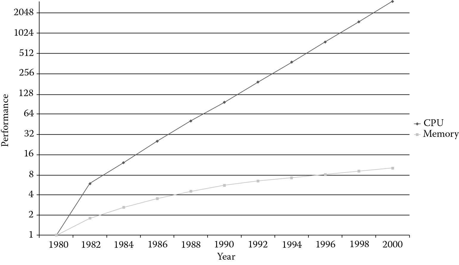
Early in the history of computers, it was thought that memory would only store the data being processed. The computer program being executed would be input one instruction at a time from punch card. However, with computers such as the ENIAC (Electronic Numerical Integrator and Computer) being able to execute 5000 instructions per second, inputting program instructions from punch cards would reduce the ENIAC’s performance to that of the punch card reader. John von Neumann was the first to conceive of the stored program computer. The idea is that a computer’s memory would store both program code and program data. In this way, the CPU would not be burdened by the slow input offered by the punch card reader. However, there is a significant problem with relying on memory (RAM) and that is that CPU speeds continue to improve substantially every year but RAM access speed improves only very gradually over the years. The result is that the CPU now has to wait on memory to respond. Figure 2.6 illustrates the enormous improvement in processor speed versus the modest improvement in memory access time. Notice that the performance increase shown on the Y axis is in an exponential scale, increasing by units of 2. For instance, between 1982 and 1986, memory access time barely increased, whereas CPU performance quadrupled. As the CPU’s performance roughly doubles every couple of years, whereas main memory access time barely increases over the years, main memory access speed lags behind CPU speed more and more with each passing year.
The CPU relies on memory at least once per instruction—to fetch the instruction from memory. Some instructions require either reading from memory (load instructions) or writing results to memory (store instructions). In such an instruction, there will be two memory accesses per instruction, one instruction fetch and one data load or store. In fact, some processors allow multiple reads and writes to memory with each instruction. If the CPU is much faster than memory, what happens? Does this ruin the processor’s performance because it is always waiting on memory?
Before continuing, we need to define RAM. RAM stands for random access memory. The idea is that we send memory an address and a read command. Memory looks up the item and returns it. Alternatively, we send memory an address, a datum, and a write command. Memory then stores the item at that location. The term “random” is meant to convey that addresses will be sent in a seemingly random pattern. The term is also meant to express that access to any address should take the same amount of time no matter which address is sent. This differentiates RAM from forms of storage that take different amounts of time depending on the location of the item being sought (tape, for instance, might require a good deal of fast-forwarding or rewinding, and disk takes time for the read/write head to be moved accordingly). Unfortunately, the term RAM is somewhat ambiguous—there are three forms of memory that all qualify as RAM.
We differentiate these forms of RAM as dynamic RAM (DRAM), static RAM (SRAM), and ROM. ROM is read-only memory. It is memory where the information being stored is permanently fused into place, so it can only be read, not written to. Most computers store the boot program in ROM along with the basic input/output system (BIOS) but little else. We will not worry about ROM in this text. Of the other two forms of RAM, DRAM is the older. DRAM consists of capacitors, which can be miniaturized to such an extent that we can literally have billions on a single chip. DRAM is also very inexpensive. DRAM, however, is relatively slow when compared to the CPU (refer back to Figure 2.6). So, on the one hand, we have an inexpensive means of providing a great deal of memory storage, but on the other hand, the access time is much slower than the CPU (by a factor of between 25 and 100!).
SRAM is built using several transistors, units known as flip-flops. We use SRAM to build both registers in the CPU and cache (pronounced “cash”) memory. Cache is a newer technology in computing than DRAM but very valuable. SRAM is far more expensive than DRAM though, so we tend to use a good deal less of it in our computers. However, SRAM is roughly as fast as the CPU, and therefore when the CPU accesses SRAM for instructions or data, the CPU is not forced to wait like it does when accessing DRAM.
This leaves us with an interesting dilemma. Since we have a small amount of SRAM, how can we ensure that when we need something from memory, it has been moved (copied) into SRAM from DRAM? For that, we design the memory of our computer into what we call the memory hierarchy. This comprises several layers where each layer going down will be slower, less expensive memory, but also of a far larger storage capacity (Figure 2.7).
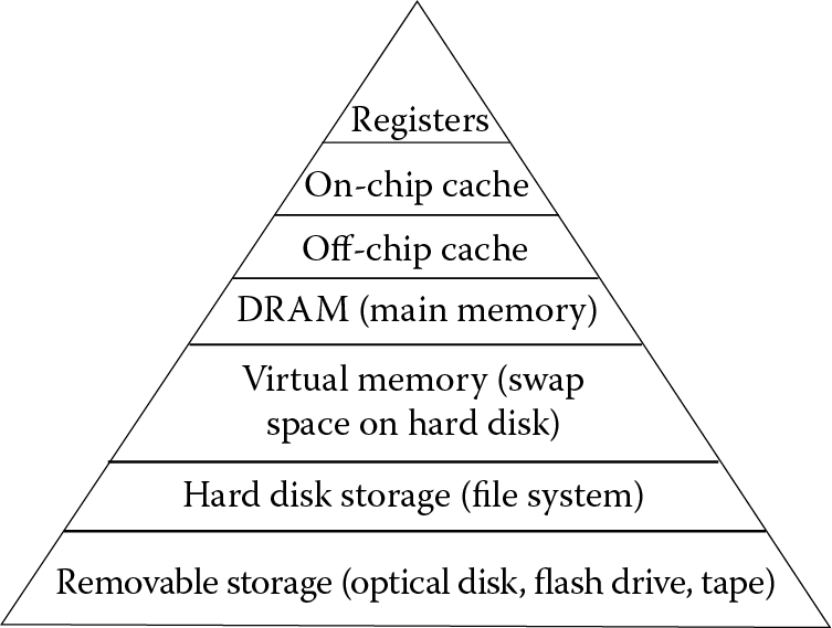
In the memory hierarchy, registers are part of the CPU. There are anywhere from a few to a few dozen registers, each able to store a word,† so a CPU might have a few dozen to a few hundred bytes of register storage. They operate at roughly the same speed as the system clock. There are often two different levels of cache: on-chip and off-chip. The on-chip cache is located on the CPU although is not in the same area of the CPU as the registers. Although on-chip cache is the same technology as registers, additional addressing hardware is needed that causes on-chip cache to be slightly slower, perhaps as much as twice as slow as register access. The off-chip cache, located separately on the motherboard, uses the same technology as on-chip cache. However, because the off-chip cache is a greater distance away from the CPU, it requires a longer time to access it, perhaps 3 to 10 times slower than the on-chip cache. Because the on-chip cache is located on the CPU itself, it must share space with the rest of the CPU. The off-chip cache can be far larger and therefore a far greater storage capacity. An on-chip cache might consist only of 32 or 64 KB, whereas an off-chip cache might be anywhere from 1 to 8 MB in size. Even so, the off-chip cache is far smaller than DRAM capacities, which today are at least 4 GB. Yet, the DRAM speed is far slower still, perhaps 25 to 100 times slower than the CPU itself.
Notice that the memory hierarchy does not end with DRAM. The programs that we run today are often larger than the size of memory itself! How then can we squeeze them into memory? Also consider that we tend to run several programs at a time. In order to handle the need for greater amount of memory than we have, we extend main memory using a concept called virtual memory. In virtual memory, whatever is not currently being used is shipped off to an area known as swap space. Swap space is stored on the hard disk in a separate area known as the swap partition. This partition is set up differently from the rest of the file system disk space—it is partitioned to be faster even though the partitioning is not as efficient in terms of space utilization. But by having it operate quickly, we can swap pieces of memory in and out as needed.
Each level of the memory hierarchy acts as a “backstop” for the next higher level. We start by loading the entire program and space for data from hard disk (or removable storage) into virtual memory and copy only the parts that are needed immediately (e.g., the start of the program) into DRAM. Then, as we begin to access instructions and data, they are copied into the on-chip and off-chip caches. Once the on-chip cache fills up, any additional items loaded into the cache first require that something be discarded.
As you move up the hierarchy, the space restrictions are greater and so discarding happens more often. Selecting wisely results in items being in the cache when the CPU needs them. Selecting poorly causes poorer performance. We refer to the efficiency of cache by the hit rate (how often what we want is found in the cache). Surprisingly, even for small on-chip caches, hit rates can be as high as 98% to 99%. As you move down the hierarchy, hit rates improve. Variations of the hierarchy have been tried including a third level of cache and including a cache with the hard disk. These variations, although more expensive, tend to improve performance.
Role of Input and Output
The I/O subsystem consists of input and output devices (including storage devices), a bus to connect the devices together and to the system bus, and interface devices such as expansion cards and ports. Strictly speaking, a computer does not need input or output devices to function. The computer program is stored in memory along with program data, and results are stored back into memory. However, without input and output devices, we are unable to interact with the computer. We cannot tell the computer what we want done, nor can we view the results.
The earliest forms of input and output were restricted to magnetic tape, punch cards, and computer printout. There was no direct interaction; instead, the user would prepare both the program code and data using a teletype device, whose results would appear on punch cards (one card per instruction or datum). The stack of punch cards would be input through a punch card reader and stored on magnetic tape. The tape would be mounted, the program and data input and executed, and the output stored back to magnetic tape. The tape would be removed and mounted onto a printer, which would print the output. This was not a very satisfying way to use a computer!
Today, of course, there are a great number of devices available to make the computer accessible in any number of situations. The key word behind I/O today is ease of use. We refer to the design philosophy of this interaction as human–computer interaction (HCI). In HCI, we view computer usage as human-centric rather than machine-centric. Table 2.1 lists some of the more common I/O devices in use today and the primary reason for their use. Storage devices are omitted from the table but would include internal and external hard disk, optical disk, flash memory, magnetic tape, and network storage devices. Network storage is commonly hard disk, accessible over a network.
Input and Output Devices
|
Bar code reader |
Input packaging information, used primarily in stores |
|
Camera |
Input video image (still or moving) |
|
Goggles |
Output video image, used primarily in virtual reality |
|
Joystick |
Input motion/pointing information, used primarily for computer games |
|
Keyboard |
Input text information, primary means of input for most users |
|
Microphone |
Input voice information, used in cases where either the user is unable to use hands or has a large amount of information to input; sometimes inaccurate |
|
Monitor |
Primary output device |
|
Mouse |
Input user interactions with GUI windowing system |
|
MIDI device |
Input of musical instrument data |
|
Pen tablet |
Input written information when keyboard is undesirable; sometimes inaccurate |
|
Printer |
Output text and/or images to paper |
|
Scanner |
Input text and/or images from paper |
|
Speakers |
Output music and sound |
|
Touch pad/point |
Alternate pointing input device when mouse is not desired (because of portability issues or health issues) |
|
Touch screen |
Alternate pointing input device when mouse and touch pad/point is not desired, primary input device for handheld devices |
|
Trackball |
Alternate pointing input device when mouse is not desired (because of portability issues or health issues), sometimes used for computer games |
In HCI, the emphasis is on promoting more natural ways of communicating with a computer. This area of study, which brings in branches of computer science, psychology, design, and health, among others, provides guidelines for more accessible computer usage. For instance, Braille output devices are available for users with visual impairments. Larger monitors and operating systems that can easily change screen resolution (the size of the objects on the screen) can also aid those with visual impairments. Microphones are often used by people who cannot use a keyboard and/or mouse.
HCI also focuses on devices that will reduce the strain placed on the human body through excessive computer interaction. Ergonomics is the study of designing systems and objects to better fit human usage. For computers, these include improved keyboards that put less strain on the human wrist, better pointing devices such as an improved mouse or a touch point, as well as improved furniture. Both keyboard and mouse usage have led many people to developing carpal tunnel syndrome, one of the many forms of repetitive stress injuries. A repetitive stress injury arises from doing similar actions over and over in such a way that it causes wear and tear on the body. For instance, using a keyboard incorrectly can strain the muscles in the wrist, leading to carpal tunnel syndrome. Poor posture when sitting in front of a computer for hours at a time can lead to other forms of stress.
The Rehabilitation Act of 1973, which authorizes grants to states that promote services for citizens with severe handicaps, has been amended (section 508) to promote accessibility in all forms of IT. The standards set forth in section 508 include guidelines for IT products including websites, software, operating systems, and hardware. For instance, all desktop and laptop computers are now required to come with expansion slots that support the various HCI devices (e.g., microphone, trackball). Operating systems are required to permit change in screen resolution to accommodate visual impairments. Government-supported websites are required to be easily traversable, for instance, by permitting the use of the tab key (or other hot keys) rather than the mouse to move from one area to another.
Aside from the Rehabilitation Act section 508, there are many other accessibility guidelines. These include the national instructional materials accessibility standards, promoted by the American Foundation for the Blind, UDL Guidelines 2.0 from the National Center on Universal Design for Learning, and the Web Content Accessibility Guidelines as recommended by the World Wide Web Consortium. Each of these focuses on different technologies, but they all promote the ideology that accessibility is important. Through HCI, information technology has become more usable to a greater population.
Although both accessibility and reduced injury are important goals of HCI, studies today primarily explore how to put the human at the center of the computer’s interaction. From a data perspective, how can we improve human ability to input into the computer? For instance, would a microphone coupled with speech recognition technology allow a human to input more accurately and quickly than a keyboard? For the processed information (output), is the monitor the best output device? Would 3-D goggles provide a more precise way of conveying information?
Issues in HCI include not only improved devices, but improvements to existing devices. Two examples are to provide higher resolution displays to make output more legible and to provide redundancy in output to ensure that the output signals are understood. Other concepts include matching mental models of the human mind, providing related information in close proximity to other related information, using visual output rather than text to better match human memory capabilities, and so forth.
One last issue with HCI is permitting the human to move away from the stationary computer and take computing with him or her. This concept, sometimes referred to as ubiquitous computing, is now available through the use of handheld devices. However, small screens do not seem to support the concepts listed above. Therefore, new I/O devices are being developed that allow us to take our computing with us. These devices combine wireless and cell phone-based technologies with some of the more advanced input and output devices such as goggles for displays, microphones for input, and headphones for audio output. Sometimes referred to as wearables, these devices will probably become commonplace over the next 5 to 10 years.
As an example of what a wearable could do, imagine that you are riding the bus. The bus provides wireless Internet access. Your wearable devices connect to your home computer through the wireless, so all processing and storage is on your home computer. Your goggles are presenting to you visual information such as text-based news or a video. Your headphones not only serve to provide you audio output, but also attempt to block sounds coming from the outside world. Your microphone allows you to speak to your computer to control what you are doing. Finally, the goggles are not entirely opaque, they are semitransparent so that you can also see the outside world as necessary (for instance, so that you can see when you arrive at your bus stop). But the goggles do more than just present an image from your computer. Your computer has been programmed to block unwanted images. And so, as you walk off the bus, you do not see the advertisements displayed on the side of the bus, instead those images are replaced with blank spots or images that you find appealing. Does this sound farfetched? Perhaps it is today, but it will not be as HCI continues to improve.
Aside from wearables, there are a number of other forms of emerging technology worth mentioning. Touch screens are obviously a large part of our lives today as they are a part of all smart phones and tablet devices. Touch screens are both input and output devices as they are displays that have sensors to note locations where a person is making contact with the screen. Touch screens have existed since the late 1960s, but were too prohibitively expensive to use in computing devices. However, today, touch screens are used not only for handheld device interfaces, but for computer games, kiosks, and medical devices, and may soon also be found as a standard interface for desktop and laptop computers. Today’s touch screens do not require a pen-based (stylus) interface and are capable of responding to multiple touches at the same time.
Virtual reality (VR) is a technology still in its infancy even though it has been around since the late 1980s. In VR, the computer creates an illusionary world and through various types of input and output devices, the human is deposited in that world. The human interacts with the virtual world based on the motion and orientation of the head, via a headset with a motion sensor, and data gloves. The user sees and hears the virtual world through goggles and headphones (Figure 2.8). In addition, a full body suit can provide the user with other forms of sensation.
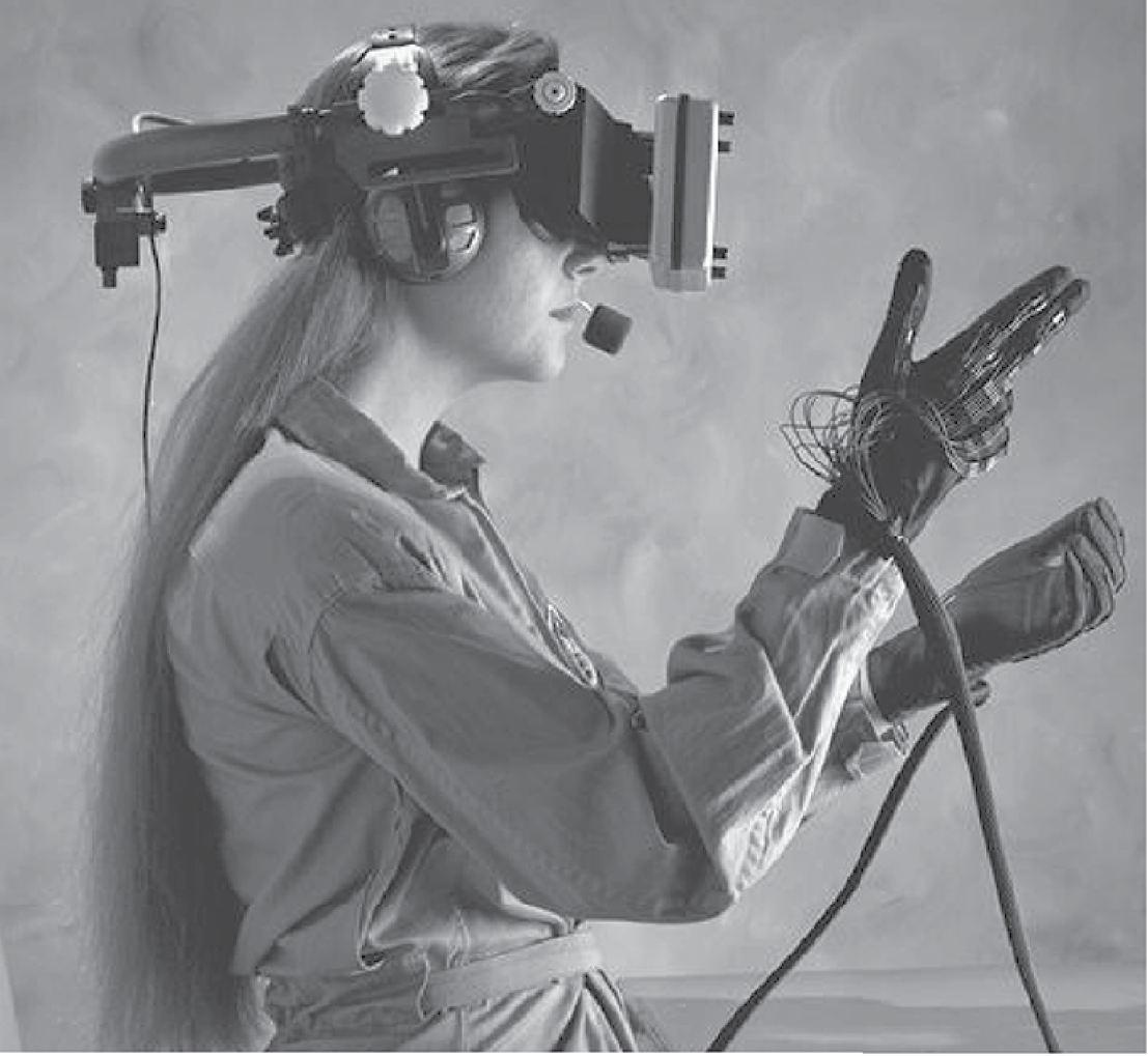
Virtual reality headset and data glove in use. (Courtesy of NASA, http://gimp-savvy.com/cgi-bin/img.cgi?ailsxmzVhD8OjEo694 .)
With VR, a human can be immersed in a location that normally the human could not reach, such as walking on Mars or walking into an active volcano, or swimming deep in the ocean. Practical uses of VR include exploration, design and analysis (imagine inspecting an aircraft that only exists in the design stage), education, and entertainment. However, in spite of the potential that VR offers, it is not commonplace because there are many obstacles to overcome. Primarily, the limitations in I/O devices to portray a realistic illusion leave a lot to be desired. Additionally, VR requires an excessive amount of computation to properly model and present an illusionary world. Thus, VR is still fairly expensive with data gloves and headsets costing between $500 and $5000 each.
One last form of emerging I/O technology worth noting is the sensor network. Sensors are devices that can sense some aspect of the environment such as temperature, water pressure, or sound vibration. Most devices that contain sensors usually have limited sensors, positioned in specific locations on the device. A sensor network is a distributed collection of sensors so that the device is able to obtain a more realistic “view” of the environment. Today, sensors are cheap enough that sensor networks are becoming more commonplace. We combine sensors with wireless communication to create a wireless sensor network, consisting of as many as a few thousand individual sensors, each of which can communicate with each other and a base computer to process the sense data. Sensor networks are found in a variety of consumer devices, vehicles, health monitoring devices, and military hardware. An entire sensor network may cost as little as a few hundred dollars. Applications for sensor networks include surveillance, monitoring atmospheric conditions (weather, greenhouse gases, air pollution), health monitoring, seismic activity, and exploration.
To wrap up this discussion of I/O devices, we also need to address two other technologies that have improved users’ abilities to connect the devices to their computers. These are plug-and-play and USB. The idea behind plug-and-play is that you are able to connect a new device to your computer at any time and that the device, once recognized by the operating system, is ready for use. Before plug-and-play, you would have to reboot your computer once you connected the new device so that the device could be recognized during the boot process. Plug-and-play was first pioneered for the Windows 95 operating system but has since become standard in most operating systems.
The most common (although not only) means of attaching a new I/O device to your computer is through the USB port. USB stands for Universal Serial Bus, a standard interface for computers since the 1990s. The USB standard defines the connectivity, which dictates the type of cable used, the method of communication between device and computer, and the power supply that will exist between the computer and device. Today, most devices can be attached via USB including keyboards, pointing devices, printers, external disk drives, smart phones, and other handheld devices. USB drives, or flash memory, give a user a decent amount of external storage (1–8 GB) that is portable. The USB port has replaced serial and parallel ports used by such devices. In addition, the USB port can supply power to the device.
Computer Hardware and Computer Assembly (Installation)
In this section, we examine the more common computer components and examine a basic assembly (installation) for windows-based desktop computers.
CPU
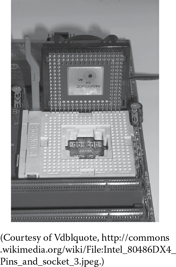
The central processing unit, or processor, is stored on a single chip, known as the microprocessor. The CPU has a number of small pins on one side of it. It is best to never touch these pins—bending them will most likely ruin the CPU. You insert the CPU into a special socket on the motherboard. You might notice that one corner of the CPU has a triangle on it. This will help you position the CPU correctly when you insert it into its socket.
Memory
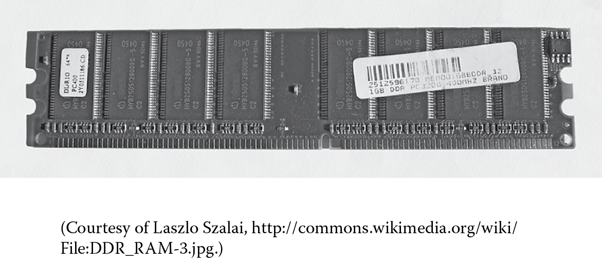
Most computer memory is stored in RAM. We usually refer to this as memory or main memory, although there are other types of memory in the computer (ROM, cache). Memory chips today come already placed on a circuit board. You slip the circuit board into a special slot on the motherboard. Again, you will have to position the circuit board correctly into the slot. If you notice in the figure, there are pins that run along the bottom of this circuit. One set of pins is longer than the other; this will help you decide the proper orientation in the memory slot.
System Unit
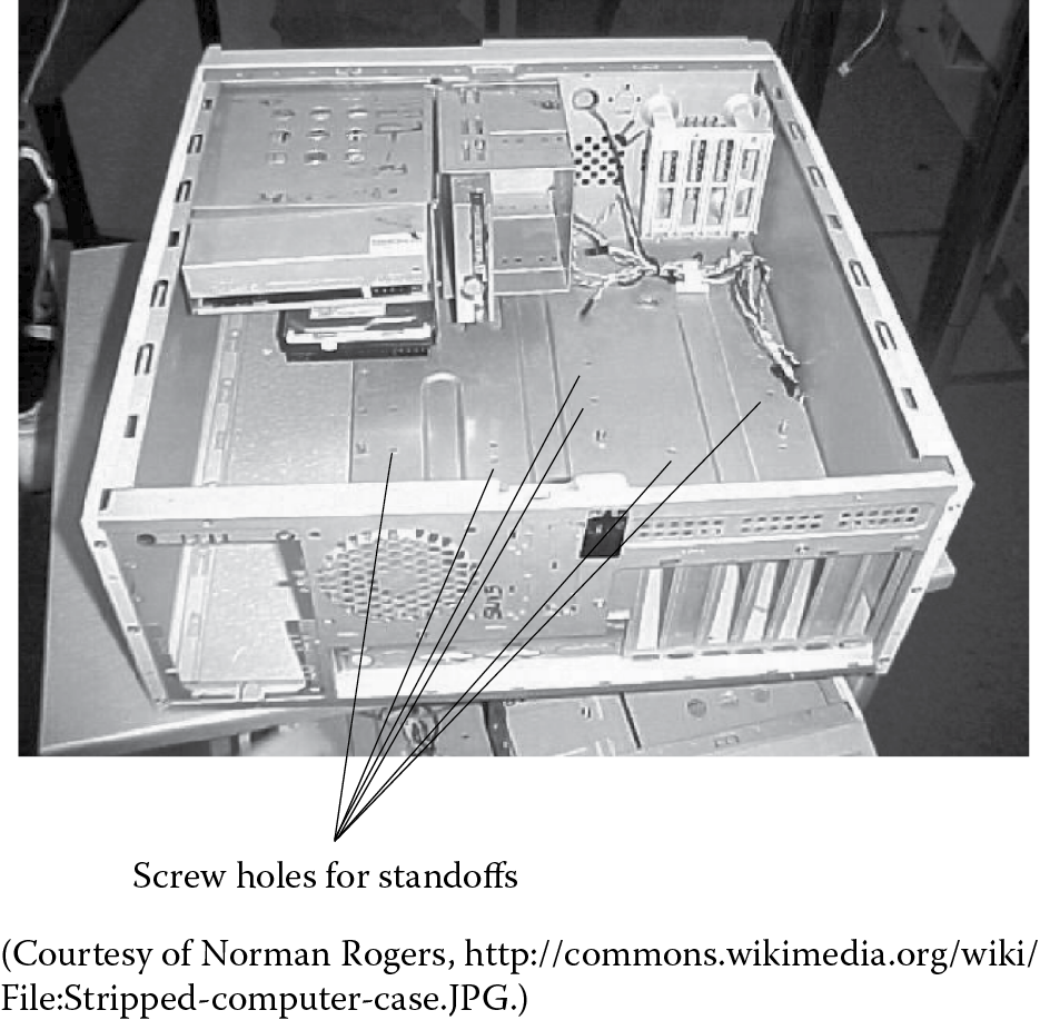
This is a case into which you will place several key components of the computer. The most important component is the motherboard. The motherboard will sit on top of “standoffs” to elevate it above the surface. It will actually be placed along one side of the system unit, not on the bottom. Looking at the system unit, you can see many screw holes; some of these will have the standoffs. Also inserted into the system unit are a power supply, a fan, and some storage devices such as an optical disk drive and a hard disk drive. There is room for other devices in the slots along the front of the system unit.
Motherboard
The motherboard provides the connections between the CPU, memory, and other components. These devices will connect to the motherboard via expansion slots and rear panel ports. The motherboard is a piece of fiberglass or plastic on which sockets and bus lines are attached. The sockets include one (or more) socket for the CPU, sockets for DRAM memory, expansion slots for cards that are interfaces with peripheral devices, connectors for storage devices, power supply connections, and ports that will stick through the rear panel of the system unit. ROM memory chips are already attached to the motherboard.

The motherboard has screw holes so that you can attach it to the system unit. As the system unit will usually stand vertically, the motherboard will actually be positioned vertically as well, so it is important that the motherboard be attached firmly. Additionally, the standoffs ensure that the motherboard does not physically touch the inner surface of the system unit. Since electrical current flows across the motherboard, if it were to touch the metallic inner surface of the system unit, this could short out the current flow resulting in a lack of current making it to the appropriate chips.
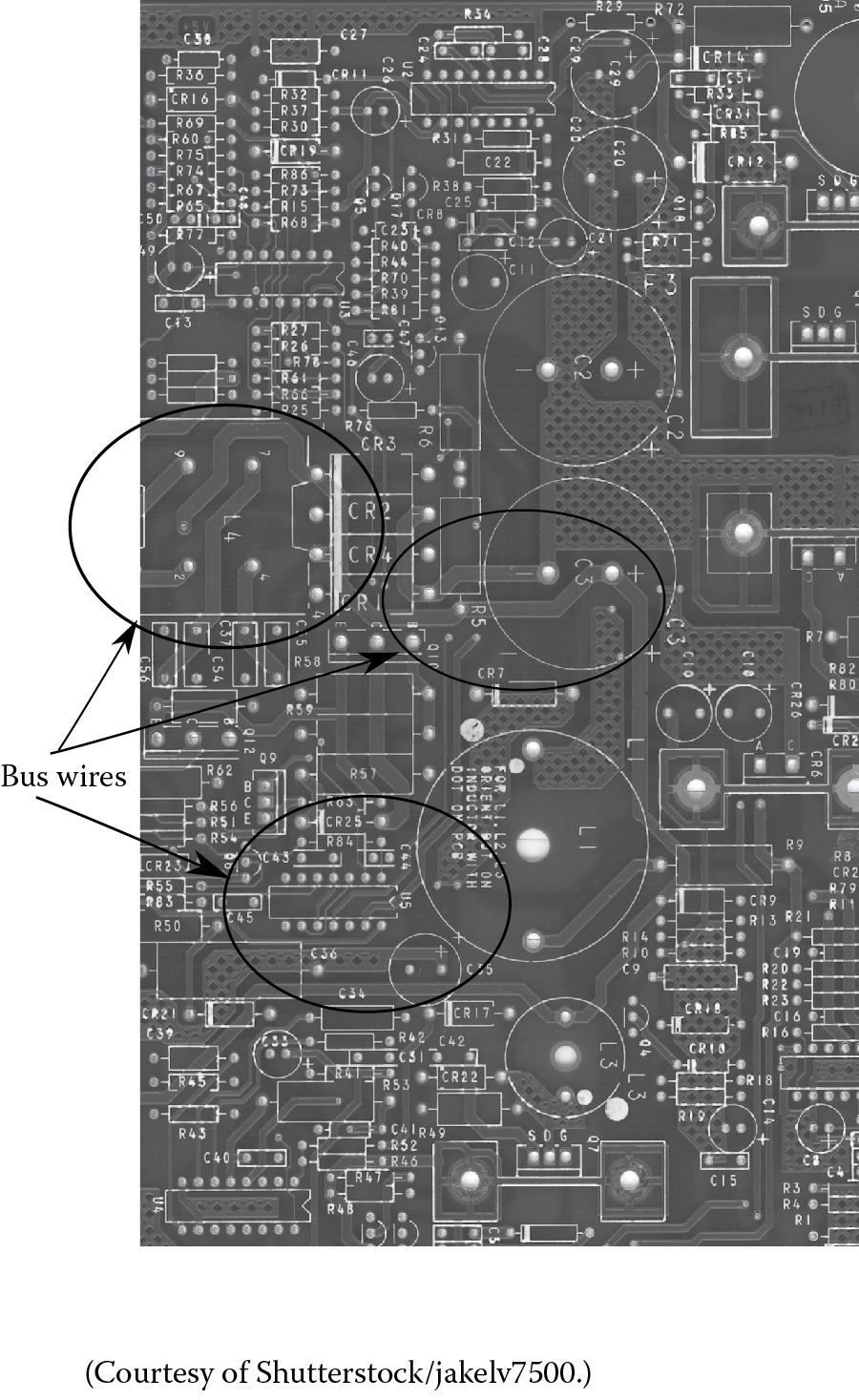
The underside of the motherboard contains “wires”—soldered lines that make up a portion of the system bus. Current flows over these lines. Therefore, it is important that these lines do not touch anything else that is metal. This is one reason why we will mount the motherboard on top of “standoffs”. This will elevate the motherboard off of the side of the system unit. Notice that the underside of the motherboard is rough (bumpy) with little pieces of hardware and solder sticking out. When you work on the motherboard, it is best to place it on top of a soft, yielding surface, but also one that will not conduct any electricity. The box that the motherboard came in would be one possibility, and the plastic bag that contained the motherboard would be another.
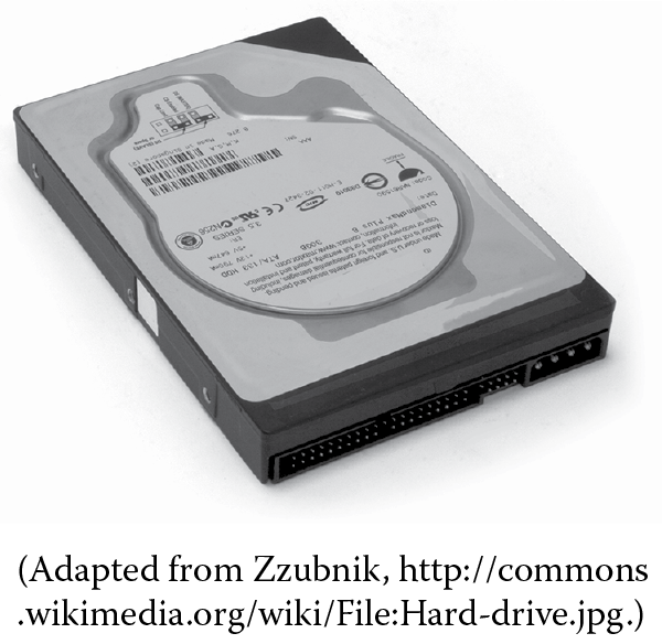
Hard Disk Drive
The hard disk is the standard unit of long-term storage. In the earliest days of computers, magnetic tape was used (reel-to-reel then magnetic tape cassettes and cartridges).
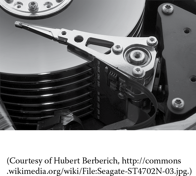
Today, the hard disk drive stores a great quantity (typical storage sizes are about 1/2 TB to a full TB). Our computers also contain optical disk drives more to allow our computers to serve as entertainment consoles (to play music CDs and movie DVDs) than for storage purposes. The hard disk drive contains several hard disk platters onto which information is stored as magnetic charges. Read/write heads move in unison over the various disk surfaces. The hard disk drive also contains the logic and mechanisms to spin the disks and move the read/write head arm.
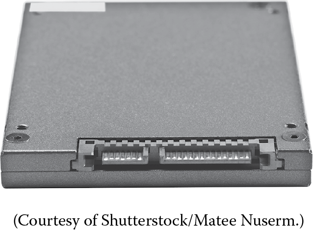
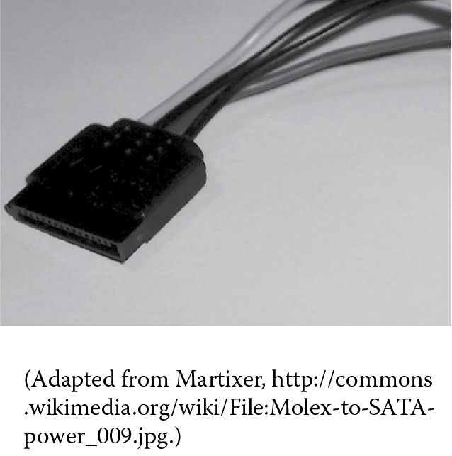
There are generally two types of drives that we use today: IDE (Integrated Drive Electronics) and SATA (Serial Advanced Technology Attachment). Shown below are the back of a SATA drive where you can see two connections, one for the power supply and one for data. To the right of the drive is a power cable for the SATA drive. Notice how the SATA connector has an “L-shape” to it, which helps you orient the connector when you plug it in.
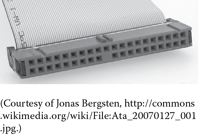
An example of the back of an IDE drive is shown below. To its right is an IDE data connector. The power connection for the IDE drive consists of four holes to match the four prongs on the left (as shown here, the drive is upside down so in fact the four prongs would be on the right) of the drive.
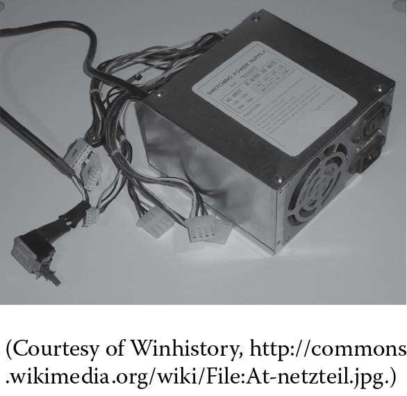
In addition to the motherboard and drive units, you will also insert a power supply unit into the system unit. The power supply unit connects to a number of cables. These cables are connected to the motherboard to power the motherboard, CPU, the display panel (on the front of the system unit), the fan, and the drives. This figure shows the cables all bundled together. You will have to be careful as you connect the various power cables to their locations on the motherboard or drives as these cables can be awkward to connect correctly such that they do not get in your way as you continue with the assembly process.
Buying a Computer
So you want to buy a computer. What are your choices? Before answering this question, you must first decide what you will use the computer for. This will help you classify which type you might need:
- Server
- Desktop
- Laptop
- Notebook
Once you have selected the type of computer, you have other choices. If you are looking at anything other than a server, your choices basically boil down to
- Macintosh
- PC running Windows
- PC running Linux
- Other (this is primarily a choice for notebook and server)
And now within these choices, you must select
- Processor type (speed, cache size, 32-bit or 64-bit)
- Other peripheral devices
Your choices here are predicated on the use of the computer, the software requirements of software you intend to use, and the amount of money you are willing to spend.
You might wonder, what about the connectors for the keyboard, mouse, and display? These connections are already part of the motherboard. You will remove a panel from the back of the system unit so that the various connectors (ports) are accessible from outside.
Now that you have seen the various components, let us look at how they go together. The first thing you should do is identify all of the components. These will include the motherboard, CPU, memory circuit boards (chips), power supply, hard disk drive, optical disk drive, screws and standoffs, a grounding strap, and tools. Although you do not have to wear the grounding strap yet, be aware that it is very important that you put it on before touching any of the electronics (motherboard, chips). To further protect the hardware, do not work on carpeting and wear lose clothes that will not retain a static charge. A static charge could damage any of the chips, most especially the CPU. In addition, keep the work area clean of clutter and debris. Do not plug in the power supply yet, and always plug the power supply in to a power strip, not directly into a wall socket

After identifying and organizing your components, the first step is to mount the power supply into the power supply bay of the system unit. You will need to remove the side panel off of the system unit. Place the power supply in its proper place and screw it in. You will also need to remove the rear port panel. This should snap right out.
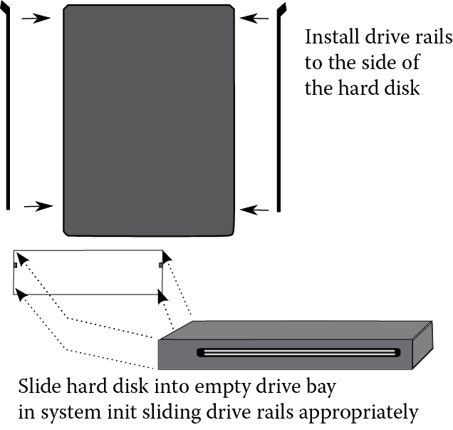
Next, you will insert the DVD and hard drive. You will have to remove the front “bezel” off of the system unit in the location of where you want to insert the DVD drive (you do not need to do this for the hard disk since the hard disk drive’s surface will not need to be visible, but the DVD drive needs to open). Depending on the type of system unit shell you have, you will either have to attach plastic rails onto the drives to slide them into their slots, or slide the drives in and attach them using the slot “arms”. Once your drives are in place, do not yet connect any cables to them. The cables would interfere with other work, so it is best to save the connections until the last steps.
Now, you will begin to assemble the components on the motherboard. For this, you need to wear a grounding strap. You should attach the lose end of the grounding strap to something metal, preferably the metal “cage” of the system unit. Using the motherboard, determine where the standoffs are needed in the system unit. Do not affix the motherboard yet, but screw in the standoffs in their proper position (again, using the motherboard to determine where—you will need to look for the screw holes in the motherboard and match then to screw holes in the side of the system unit).
The first component to insert onto the motherboard is the CPU. Make sure you have the CPU aligned properly (look for the arrow), lift the locking lever bar, flip up the CPU socket lid, slip the CPU into its socket, lower the lid, and then lock the lever into place.
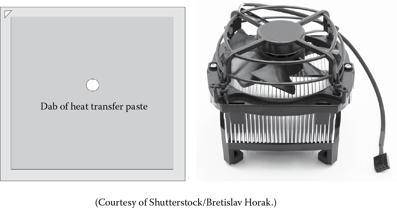
Next, you will affix the CPU’s cooling unit. First, you need to place a dab of heat transfer paste onto the outer surface of the CPU. The amount you place onto the CPU is small, about the size of a small pea. Next, orient the cooling unit so that its four connectors (pegs) are positioned over the four holes surrounding the CPU socket. Make sure that the unit is oriented so that the power cord can easily fit into the power socket on the motherboard. Once it is positioned correctly, push down on each of the four pins one at a time. Once all four pins have been pushed through the motherboard, lift up the motherboard to confirm this. Then, turn each of the pins as indicated on the surface to lock the pins in place.
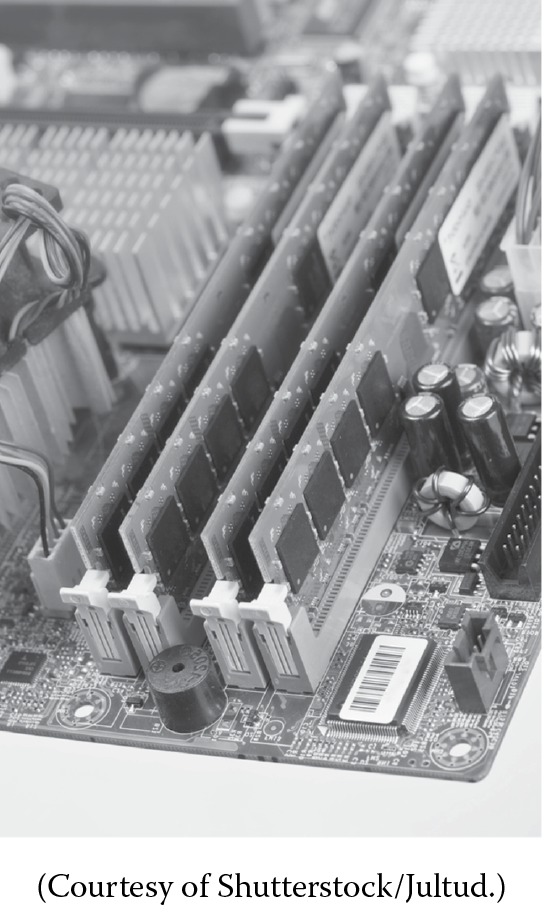
Next, take a memory circuit board and insert it into one of the memory slots. Make sure that the board is aligned properly by looking for the gap in the pins and match it to the gap in the slot. Make sure the tabs along the side of the slots are “open”. Slide the circuit board onto the opening and then using your thumbs only, press down until you see the tabs close automatically. You would repeat this step for each memory circuit that you wish to add to your computer.
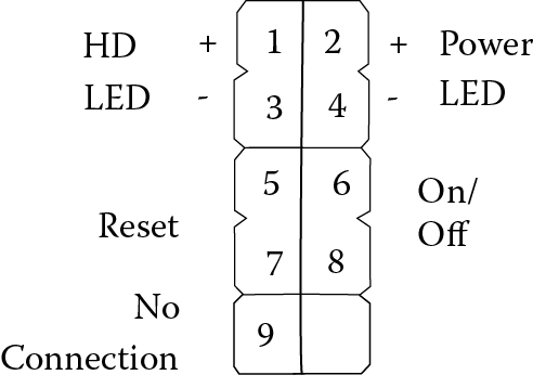
With these units in place, you can now screw the motherboard into place on the standoffs inserted earlier. To finish off the installation, you will now need to make all of the connections between the power supply unit, drives, fan, and motherboard. First, find the cable that has four 2-pin connectors (note: depending on the power supply unit, this might be a single eight-pin connector). The attachments will be shown on the motherboard installation document. For instance, the drawing below indicates the connections to power the disk drive LED, the reset (reboot) button, the power LED, and the on/off switch. Failure to connect the connectors to the proper pins will result in these components not functioning. In the diagram below, pins 1/3 are used for the hard disk drive LED. Pins 2/4 power the on/off LED. Pins 5/7 are used for the reboot button. Pins 6/8 are used for the on/off button’s light. Finally, pin 9 does nothing.
Next, connect your drives. You will probably have two drives to connect, an optical drive and a hard disk drive. Chances are, the hard disk is an IDE as IDE drives are more common in PC-style computers. The optical drive may be either SATA or IDE. Identify the type to determine which plugs to use. First, insert the drives into available bays in the system unit. You will probably want to insert the optical drive on top. This is because the optical drive will interface with the outside world so it is more common to have it appear near the top of the system unit. You will have to remove the cover over that bay so that the optical drive is accessible from outside. Different system units will have different types of bays. Commonly though, all you need to do is slide the drive into the bay and then turn the key on the side of the bay.
Once both (or all) drives are in their bays, you must connect them to the motherboard and the power supply unit. Find the appropriate power cable to attach to the power supply and the appropriate data cable to connect to the motherboard. The last connection is to plug the fan power cable into the power supply cable and to connect this to the motherboard. At this point, you can plug in the power supply unit to both the computer and the surge protector. Make sure the surge protector is plugged into an electrical outlet and turned on. Now you can boot your computer!
If the computer successfully boots, it will boot to the ROM BIOS but because there is no operating system on your hard disk, it will not reach windows. If you have successfully assembled your computer, insert a Windows installation CD into the optical drive, shut down the computer, and reboot. Once the computer has booted to ROM BIOS, you can go through the Windows installation (this is briefly covered in Chapter 4). Congratulations!
Further Reading
Computer science and computer engineering programs typically require a course on computer organization and architecture. Texts for such courses go well beyond the introductory level presented in this chapter. Among the topics covered in such classes are Boolean algebra and circuit design, binary representations and arithmetic (which we introduce in Chapter 3), CPU implementation details and performance, cache and DRAM technologies, and the I/O system. The seminal texts are the following:
- Patterson, D. and Hennessy, J. Computer Organization and Design: The Hardware/Software Interface. San Francisco: Morgan Kaufmann, 1998.
- Hennesey, J. and Patterson, D. Computer Architecture: A Quantitative Approach. San Francisco: Morgan Kaufmann, 2012.
The first text is primarily targeted at juniors in college, whereas the latter is aimed at seniors and graduate students. Both of these texts are challenging even for the brightest computer science majors. Other computer organization and architecture textbooks include the following, the third of which might be one of the more accessible books particularly for non-majors:
- Clements, A. The Principles of Computer Hardware. New York: Oxford, 2000.
- Hamacher, C., Vranesci, Z., Zaky, S., and Manjikian, N. Computer Organization and Embedded Systems. New York: McGraw Hill, 2012.
- Null, L. and Lobur, J. The Essentials of Computer Organization and Architecture. Sudbury, MA: Jones and Bartlett, 2012.
- Stallings, W. Computer Organization and Architecture: Designing for Performance. Upper Saddle River, NJ: Prentice Hall, 2003.
- Tanenbaum, A. Structured Computer Organization. Upper Saddle River, NJ: Prentice Hall, 1999.
You can find a nice demonstration on the fetch–execute cycle at http://www.eastaughs.fsnet.co.uk/cpu/execution-fetch.htm. Additionally, the website http://courses.cs.vt.edu/csonline/MachineArchitecture/Lessons/CPU/Lesson.html provides a nice diagram of the most important parts of a CPU along with a description of how they are used during the fetch–execute cycle.
One of the best sources for comparing CPU performance on benchmarks is the website www.cpubenchmark.net. You can also find useful pricing comparisons of computers and computer hardware at www.pricewatch.com.
Texts covering just the memory hierarchy tend to cover design and algorithms for efficient memory usage or leading-edge technology with DRAM and SRAM. The following text though will shed more light on the role of the components that make up the memory system:
- Jacob, B. and Wang, D. Memory Systems: Cache, DRAM, Disk. San Francisco: Morgan Kaufmann, 2007.
There are a number of texts dealing with input, output, HCI, and related topics, some of which are listed here.
- Dargie, W. and Poellabauer, C. Fundamentals of Wireless Sensor Networks: Theory and Practice. Hoboken, NJ: Wiley, 2010.
- Dix, A., Finlay, J., Abowd, G., and Beale, R. Human–Computer Interaction. Englewood Cliffs, NJ: Prentice Hall, 2003.
- Heim, S. The Resonant Interface: HCI Foundations for Interaction Design. Reading, MA: Addison Wesley, 2007.
- Kortum, P. HCI Beyond the GUI: Design for Haptic, Speech, Olfactory and Other Nontraditional Interfaces. San Francisco: Morgan Kaufmann, 2008.
- Lumsden, J. Human–Computer Interaction and Innovation in Handheld, Mobile and Wearable Technologies. Hershey, PA: IGI Global, 2011.
- McCann, J. and Bryson, D. (editors). Smart Clothes and Wearable Technology. Cambridge: Woodhead Publishing, 2009.
- Salvendy, G. (editor). Handbook of Human Factors and Ergonomics. Hoboken, NJ: Wiley, 2006.
- Sherman, W. and Craig, A. Understanding Virtual Reality: Interface, Application and Design. San Francisco: Morgan Kaufmann, 2002.
The following government-run website details section 508 of the Rehabilitation Act of 1973, describing accessibility standards: http://www.section508.gov/index.cfm.
This chapter also provided a brief introduction to personal computer components and assembly. There are numerous books on the topic such as
- Chambers, M. Build Your Own PC Do-It-Yourself for Dummies. Hoboken, NJ: Wiley, 2009.
- Heaton, J. Build a Computer From Scratch. St. Louis, MO: Heaton Research, Inc., 2006.
- Majlak, D. Building Your Own Computer. No Frills, No Filler, Just Answers (a Kindle book). Seattle, WA: Amazon Digital Services, 2011.
- Mueller, S. Upgrading and Repairing PCs. Indiana, IN: Que, 2011.
- Thompson, B. and Thompson, B. Building the Perfect PC. Massachusetts: O’Reilly, 2010.
Although we briefly introduced programming, we will cover that topic in greater detail later in the text.
Review Terms
Terminology used in this chapter:
Accessibility Input
Accumulator (AC) Instruction register (IR)
Assembly program IPOS cycle
Address bus Load
ALU Megaflops
Bit Memory
Bus Memory chips
Byte Memory hierarchy
Compiler MIPS
Control bus Mother board
Control unit Off-chip cache
CPU On-chip cache
CPU cooling unit Output
Data bus Power supply
Decode Processing
DRAM Processor (CPU)
Ergonomics Program counter (PC)
Fan Read
Fetch–execute cycle Register
GHz SATA drive
Grounding strap Sensor network
Hard disk drive SRAM
HCI Standoffs
Hit rate Status flags (SF)
IDE drive Storage
Store Virtual reality
Swap space Wearable
System unit Word
Virtual memory Write
Review Questions
- What happens during the fetch stage of the fetch–execute cycle?
- What happens during the decode stage of the fetch–execute cycle?
- What happens during the execute stage of the fetch–execute cycle?
- What is a load?
- What is a store?
- What is an operand?
- What is the ALU? What are some of the circuits in the ALU?
- What does the control unit do?
- What does the PC store?
- What does the IR store?
- What does the AC store?
- Is the AC the only data register?
- What is moved over the data bus?
- What is moved over the address bus?
- What is moved over the control bus?
- Why does a processor’s GHz rating not necessarily tell you how fast it is?
- What is MIPS and how does it differ from GHz?
- What is Megaflops and how does it differ from MIPS?
- What is a benchmark?
- What is the memory hierarchy?
- Which form of memory is faster, DRAM or SRAM?
- Why are there both on-chip and off-chip caches?
- What happens if the CPU looks for something at one level of the memory hierarchy and does not find it?
- Where is virtual memory stored?
- What were the forms of input and output found in early computers?
- What is HCI? What does it study?
- What is a repetitive stress injury?
- What types of input and output devices could you use as wearable technology?
- What are some of the applications for virtual reality?
- Why is it important to wear a grounding strap?
- What might happen if you discharge static while working with the motherboard?
- Why should you install the CPU onto the motherboard before installing the motherboard into the system unit?
- What does the CPU cooling unit do? Why is it necessary?
- When installing a storage drive, how does the SATA data connector differ from the IDE data connector?
Discussion Questions
- How important is it for an IT person to understand the functions of individual computer components such as the role of the CPU and memory? How important is it for an IT person to understand concepts such as cache memory, pipelining processors, the use of the bus, the fetch–execute cycle, and the use of registers? How important is it for an IT person to understand the differences between SRAM, DRAM, and ROM?
- As an IT person, do you ever expect to program in assembly language? If so, provide some examples and if not, explain why not.
- Which is more significant in IT education, understanding the function of the hardware of the computer or understanding how to assemble (build) a computer? Explain.
- Most people believe that the processor’s clock speed is the most important factor in a processor’s performance. Discuss all of the factors that can impact the performance of a processor. Rank your factors in the order that you feel will have the most significant impact on performance. Where did the clock speed rank?
- In HCI, why do they need to study human psychology to design improved I/O devices?
- For the input and output devices listed in Table 2.1, which ones could cause repetitive stress injuries? Which ones might you identify as replacements to prevent repetitive stress injuries?
- Provide a list of five ways that you might use virtual reality in your day-to-day life.
- You work for a large organization. Your employer asks you to put together the specifications for new desktop computers for the employees. As these are work computers, there will not be a high demand on multimedia performance, but instead there is a desire for ease of use, efficient communications, and large storage. Put together a specification in terms of what you would look for, including platform (e.g., Windows, Mac, Linux), processor type and speed, amount of cache, memory, word size, and secondary storage. What other factors will impact your decision?
- Imagine that you are assembling your own computer as described in “Computer Hardware and Computer Assembly (Installation)”. You have completed the assembly, plugged in the computer and turned on the power switch. Nothing happens. What are some of the possible problems that might have occurred during assembly that will prevent the computer from booting?