
Chapter 1 showed the current interest in parallel or interleaved converters used for grid interfaces or motor drives. This interest has risen due to the continuous development in power semiconductor technologies leading to high-power single-die insulated gate bipolar transistors (IGBTs).
The first step toward parallel converters was hybrid (custom) IGBTs. These modules parallel IGBTs at silicon level and have many advantages. First, these chips and gate resistors are placed very close together, reducing parasitic inductance between chips. This ensures uniform temperature distribution across the chips inside the package.
A layer of thick copper directly bonded on a ceramic substrate forms the conduction path for the emitter current and the thermal spreading layer for the heat from the IGBT chips. The IGBT chips are mounted via solder on this copper layer. The ceramic substrate can be alumina, aluminum nitrite, or beryllium oxide, materials with good thermal conductivity and voltage isolation up to 6000 V. Both thermal conductivity and voltage isolation are better than the thermal pads used for isolation in parallel discrete devices.
During the design of a new power stage, a practicing engineer has to decide whether to use hybrid (custom) IGBT modules or equivalent discrete devices. Here are some points to consider:
• Hybrid (custom) IGBT modules are advantageous when more than five chips are considered. Their advantages lie in size, electrical isolation, thermal management, cost of the whole system, and the lack of noise owing to switching. The last advantage saves the need for extra bus capacitance.
• Discrete devices are advantageous when two or three chips in parallel are required to develop a design. They ensure that the smallest footprint with both electrical isolation and parasitics is manageable.
The next possibility consists of paralleling IGBTs for high-current applications, as shown in Figure 14.1. There is an obvious engineering question whether it is better to realize a high-current switch by paralleling discrete devices or by a single higher rated device.
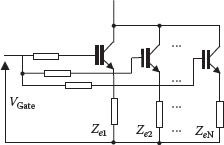
FIGURE 14.1 Parallel IGBTs.
Which solution is better to carry out a 1200 A, 1200 V switch: A high-power 1200 A IGBT or four low-power, parallel-connected 300 A IGBTs? To respond, we use a numerical example and datasheet comparison, using datasheet information from Powerex IGBTs. Further, ripple differences and different snubber requirements for both devices will be ignored.
Thermal features:
• IGBT/Diode thermal resistances of 0.13/0.18 [C/W] (300 A) versus 0.022/0.050 [C/W] (1200 A).
• Heatsink touch areas of 163.67 sq. in (300 A) versus 133.01 sq. in (1200 A).
Diode recovery loss:
• 300 A device: Trr = 250 ns, Qrr = 17.6 μF
• 1200 A device: Trr = 300 ns, Qrr = 9.0 μF
Switching loss and conduction loss: From the datasheet information regarding switching and conduction losses, one can conclude that paralleling power semiconductor switches represents a competitive solution for building three phase power converters (Figures 14.2 and 14.3).
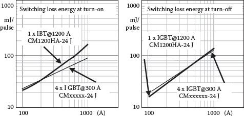
FIGURE 14.2 Switching loss at turn-on and turn-off.
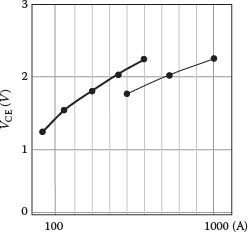
FIGURE 14.3 Conduction loss for both solutions: (left) 1200 A device, (right) 4 × 300 A device.
14.2 HARDWARE CONSTRAINTS IN PARALLELING IGBTs
Having demonstrated the suitability of parallel connection of IGBTs, ask for understanding the limits of the practical implementation. The idea of paralleling IGBT devices is based on using low-power devices that share currents equally. When the sharing is not equal, one of the currents may go beyond the rated value for that particular IGBT. Special care should be taken to avoid current mis-sharing so that the IGBT can be protected.
Differences in the current level can occur in steady state or in dynamic operation. The steady-state current imbalance is produced by different Vce(Ic) characteristics as well as by the differences in the circuit parasitic resistances. Differences in the turnon and turn-off imbalances are produced by the distribution of the module transconductance characteristics as well as by the differences in parasitic inductances. The operation is influenced by temperature imbalance and thermal instability. Each of these sources of instability is discussed next.
Two IGBTs cannot have identical characteristics due to technological dispersion. The ON-time Vce (Ic) characteristics are shown in Figure 14.4 and they can be approximated for each of the two parallel IGBTs by:
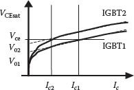
FIGURE 14.4 Sketch of the Vce(Ic) characteristics for two parallel IGBTs.
(14.1) |
Reporting each individual current to the total current of the parallel IGBTs yields
(14.2) |
Observing these two equations shows that the device with the lower Vce carries most of the current. Moreover, the total current is lower than Np * Ir due to the characteristic dispersion of a number of Np IGBT devices. Higher temperature allows better current sharing. For instance, imbalance in static characteristic represents 15% at 25°C and 5% at 125°C.
To measure and match sets of IGBTs with close Vce (Ic) characteristics, semiconductor manufacturers like Powerex came up with a special marking for different levels of the saturation voltages.
Example: … C: 1.70–1.95 V D: 1.90–2.15 V
After the design has been matched to IGBTs within the same ratings, a derating coefficient should be used to select design and device. The value of this coefficient depends on the semiconductor family as shown in Table 14.1.
A static derating factor can be defined as
(14.3) |
and it can be estimated with an empirical relationship:
(14.4) |
where Np is the number of parallel devices and x is the mis-sharing factor, which is equal to 0.10 for 250 and 600 V devices, 0.15 for 1200 V devices, and 0.20 for 1700 V devices (Figure 14.5).
TABLE 14.1
Derating of Different IGBT Families
250 V Trench Gate |
10% |
600 V |
10% |
1200 V and 1400 V |
15% |
1700 V |
20% |
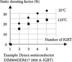
FIGURE 14.5 Dependence of the static derating factor on the number of IGBTs.
Parasitic resistances within the circuit are the second factor that can influence current sharing during IGBT’s ON-time. Mounting, busbar, and terminal connection of IGBT devices introduce parasitic resistances in both emitter and collector. The emitter resistance has a greater effect on current sharing as it influences the gate circuitry too. Depending on the emitter resistance, there will be a voltage drop on the emitter that decreases the actual gate control voltage (VGE = Vcontrol − VRE). This changes the IGBT output characteristics and modifies the appropriate collector current. Different IGBT characteristics define different currents for the same collector–emitter voltage. To reduce this imbalance, it is necessary to make the wiring on the emitter as short and uniform as possible. This reduces parasitic resistances.
It is also important to analyze current sharing during turn-on or turn-off transients. The output IGBT characteristic (Vce-Ic) does not have any direct influence on the transient turn-off voltage imbalance. In contrast, the transconductance characteristic (Figure 14.6) determines the current sharing during transient.
If the same gate conditions are ensured for both IGBTs, the device with the largest value of transconductance (steeper characteristic) carries a larger current and incurs the highest switching loss. A dynamic derating factor analogous to a static derating factor can be defined, and the comparison is shown in Figure 14.7.
Dynamic current sharing is better than static current sharing. However, dynamic sharing is more sensitive to external circuit factors, such as the stray inductance in the gate-emitter circuit loop. The transient current passes through parasitic inductances in the emitter and decreases the effective gate voltage. Different values of the emitter inductance lead to different voltage drops in the gate circuitry, producing different lengths of delay of the transition and different shapes of the current. To reduce this imbalance, it is necessary to make the wiring on the emitter as short and uniform as possible (Figure 14.8).
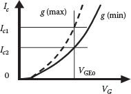
FIGURE 14.6 Transconductance characteristics.
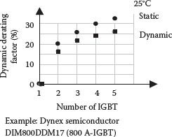
FIGURE 14.7 Dynamic derating factor in comparison with the static derating factor.
Another improvement is related to the way the gate driver should be connected. It is better to use the same gate driver with separate gate resistors to eliminate the risk of parasitic oscillations. Further, the gate resistors should be tied closely through the gate control terminal with a separate emitter pin for gate control.
Finally, there is the effect of temperature imbalance. All IGBT characteristics depend on temperature and the current sharing between two or more parallel IGBTs is influenced by their individual temperature at the junction. Examples of temperature dependence of each characteristic can be seen in any IGBT datasheet.
Temperature has some influence on current sharing in steady-state conditions. An immediate solution is to use a common heatsink for all parallel IGBTs to keep temperature spread within 10°C. The common heatsink introduces a thermal feedback between junctions. The IGBT with a higher power dissipation has a higher temperature and influences the temperature of the other through the common heatsink. The operation point of the second IGBT changes and current sharing is modified. Even if the temperature coefficient is negative for all devices, the IGBT with the lower voltage drop has a lower temperature coefficient. Lower voltage drop also implies larger current share. Both current and temperature are increasing and this is producing the decrease of the voltage drop and current compensation (Figure 14.9).
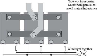
FIGURE 14.8 Emitter connection for reduced parasitics.
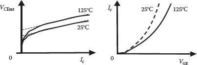
FIGURE 14.9 IGBT characteristics.
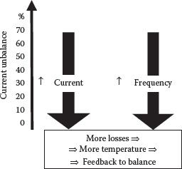
FIGURE 14.10 Current unbalance dependence on operation current and frequency.
Figure 14.10 presents this idea schematically.
14.3 GATE CONTROL DESIGNS FOR EQUAL CURRENT SHARING
Modern solutions using active gate control for static or dynamic current balancing are shown in Figure 14.11. They require high bandwidth analog processing of the sense current feedback. The levels of the gate voltage and current are controlled during the ON-time of each individual IGBT, whereas the delay of the transient is controlled in a dynamic manner.
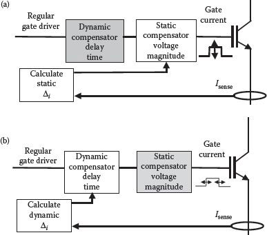
FIGURE 14.11 Gate driver control for current sharing. (a) Static current balancing. (b) Dynamic current balancing by delaying turn-on and turn-off moments.
The manufacturing volume in high-power applications is not very large and many projects end up with a unique prototype or a very short product series. As high-power devices require a special or individual design, many engineers are tempted by parallel low-power hardware. Paralleling IGBTs or MOSFETs has already been discussed earlier in this chapter, but this is not always a convenient option as the power stage needs a new design and package anyway. However, paralleling power stages is a very easy and cheap approach. The effort lies in adapting the existing control system to paralleling [3]. This is mainly done through software and the physical effort is thus limited.
Whilst there are many engineering teams which have tried parallel operation in their R&D laboratories, only a few manufacturers tried to have a systematical analysis of this new solution and to review its use in larger scale volume products. The idea is to use power converter modules from an existing series production and to add especially manufactured hardware that can support parallel connection of these modules, while using revised or additional software.
There are two possible paralleling approaches: through galvanic isolation and by direct connection on the DC side. All solutions with isolation use separate power supplies for each power converter and transformers for adding up the paralleling effects. Such a system becomes expensive and bulky, with a decreased efficiency and seriously limiting the number of parallel devices.
The second approach is based on direct connection on the DC side with interphase reactors on the load side. The control system must ensure equal current sharing [4,5,11]. The instantaneous output voltages are not equal even if their average value is. This implies different voltage levels on each side of the inter-phase reactors. This voltage drop produces circulation currents between modules that increase the required rating for the power semiconductor devices.
What are the major challenges to direct connection of power converters? Design of inter-phase reactors is limited by constraints of steady-state or transient operation. Steady-state ripples require a large inductance to limit them and reduce the IGBT conduction losses and filter losses. A smaller value of the inductance is preferred to provide a large current slew rate. The selected inductance should support the whole DC bus voltage over the sampling interval while producing a maximum ripple variation of less than a specified amount. Moreover, this inductance should limit the circulation currents on fundamental frequency owing to difference in the reference waveform of the paralleled/interleaved power converters [6,9,10,12]. Finally, a some-what smaller value is usually selected from these constraints to favor dynamic performance and to allow a reasonable circulating current.
There are different possible connections between power stages. The way the interphase reactor becomes part of the circuit is shown in Figure 14.12.
Separate inductors or mid-point inductors are often used. New solutions employ coupled inductors with direct or inverse coupling. Analysis of directly coupled or inversely coupled inductors reveals the value of the equivalent inductance at its terminals.
(14.5) |
Another alternative is to spread the reactor inductance between the AC and DC sides to improve the harmonic filtering on the AC side. This idea is adapted from the conventional diode rectifiers where power structures above 15 kW have inductors on both AC and DC sides.
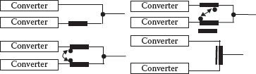
FIGURE 14.12 Different connections of the inter-phase reactor.
The major tasks of the control system are [4,5,11]:
• To equalize current sharing
• To limit circulating currents
As always, design of the control system is based on the load character. An inductive load (Figure 14.13a) suggests an open-loop control based on the switchingpattern selection, as the voltage on the load-side node is not well defined and it forms a section of inductances. In contrast, capacitive or strong voltage source character of the load (Figure 14.13b) implies a firm closed-loop control as the voltage across the load is well defined.
14.4.3 CONVERTER CONTROL SOLUTIONS
The selection of the sequence within the pulse width modulation (PWM) of all parallel converters is important. First, a single PWM circuit can be built and the same switching sequence can be used to control all parallel converters. The drawback of this solution is the difficulty of defining separate protection circuits for each power stage. Moreover, any difference in the inter-phase inductors can create zero-sequence circulating currents.
A second solution uses different control hardware on each power converter leading to almost identical PWM patterns while retaining the individual protection circuitry of each power converter. The drawback consists of not having too much improvement in the ripple during operation.
The third solution implies the control of the parallel structure by considering all possible switching states. Such an approach is limited to a small number of parallel converters to retain the number of states to a minimum. Let us herein consider the case of only two power converters. Different switching patterns in the two converters produce different circulation currents through inductors. Each difference in the PWM pattern results in a voltage drop across the inter-phase inductances and a change in current owing to the inductive nature of the load. In contrast, identical patterns in both converters maintain the same current error. These circulation currents can be produced by the difference in the reference waveforms due to the control loops, difference in the active vectors used at a given moment, or differences between the zero states used by each individual converter. Importantly, the effect of the difference in the active vectors used at a given moment can be corrected by conventional (d, q) control.
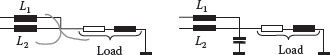
FIGURE 14.13 Different load types.
FIGURE 14.14 Switching states.
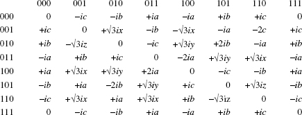
The voltage vectors derived from all switching states can be seen in Figure 14.14. Generation of any PWM uses a combination of these vectors very similar to the Space Vector Modulation (SVM) presented with the conventional three-phase six-switch converter. Each state of the system exposes different inverter legs to circulation currents. The rate of change of these circulation currents leads to changes in the zero sequence current. The rate of change of the zero sequence current is presented in Table 14.2. Table 14.3 shows changes in the cross-currents.
Once this converter analysis has been accomplished, goal is to suppress current harmonics while providing small dΔi/dt variation. The switching pattern is selected to minimize both cross-currents and zero-sequence currents with the data from previous tables. First, the cross-current vector is defined in one of the seven regions formed as complex plane sectors and a small region near zero while the zero sequence current is compared with a small window comparator to detect values from Table 14.2. The currents should remain within some tolerance margins throughout the operation (Table 14.4).
TABLE 14.3
Zero Sequence Currents Function of the Switching Table
Each inductor current on each power converter can be controlled individually or on the three-phase concept of (d, q, 0) control (Figure 14.15). Generally, a system of N identical subsystems can be transformed into a set of state equations described by a vector that is the average of the N subsystems. This creates a common-mode system that describes the dynamics of the average vector and it is used to define the control of the output voltage. Deviations from the average vector of all subsystems form another set of N − 1 state vectors adding up to zero. The system dynamics are therefore described by the deviation from the average vector through this set of N − 1 state vectors.
The proportional-integral (PI) controller can have any internal structure as discussed in the relevant chapter. The gains and limits of each current controller can be defined with the equivalent circuits on (d, q) coordinates. Understanding these gains and limits is very important as the paralleling modifies the structure of the plant model and the closed-loop transfer function. Depending on the direction of the power transfer, these equivalent circuits correspond to buck or boost DC/DC converters.
TABLE 14.4
Cross-Currents i1 − i2
“+” = Increase on axis; “–” = Decrease on axis.
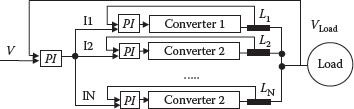
FIGURE 14.15 Structure of the control system.
14.4.5 SMALL-SIGNAL MODELING FOR (D, Q) CONTROL IN A PARALLEL CONVERTER SYSTEM
Separate equivalent circuits in quasi-DC variables are considered on the (d, q)-axes (Figure 14.16). They help in deriving a small-signal model with a control variable D (duty cycle) on each axis (Figure 14.17). Dd and Dq are duty cycles on (d, g)-axes and m is the converter modulation index so that The small-signal model is derived from the state variable equations that have all inductor currents and the capacitive output voltage as state variables (all measured in the power transfer direction).
(14.6) |
Simplified control functions are presented next. A more detailed analysis including all the instabilities due to nonlinearity and nonminimum phase system characteristics are provided on [1,2]. The big difference between current control of a single converter and current control of parallel-connected converters is seen in a different model of the plant (Figures 14.18 and 14.19).
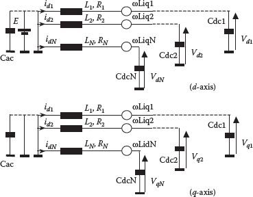
FIGURE 14.16 Boost DC/DC converter. (From Neacsu, D.O., Wagner, E., Borowy, B. 2002. 37th IAS Annual Meeting. Conference Record of the Volume 3, 13–18 October, pp. 1958–1965. With permission.)
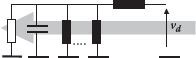
FIGURE 14.17 Equivalent circuits on (d, q)-axis.
Let us first analyze each (d, q) equivalent circuit when it behaves as a DC/DC buck converter and the small signal model of the equivalent load that results from Figure 14.20. Transfer function from duty cycle to the inductor current:
(14.7) |
The inductances of the other converters introduce a dumping effect. The modulation index to inductor current transfer function is different for each interleaved stage. The huge difference from the single-stage case is the integrative character in low frequency [7,8].
The (d, q) modeling for the power transfer through a boost DC/DC converter is shown in Figure 14.19 and the small signal model is accordingly derived. Transfer function from duty cycle to the inductor current is also shown in the figure.
Figure 14.19 shows that a change in the first converter duty cycle determines a change in the inductor L1 current, followed by a change of the load voltage across the capacitor CL. The voltage on the load changes currents through the other inductors and a feedback change in the output capacitor voltage occurs. The duty cycle to inductor current transfer function can be calculated based on the small signal equivalent circuit:
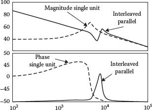
FIGURE 14.18 Bode plots for the buck converter model.
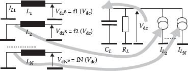
FIGURE 14.19 Equivalent circuit for parallel connection of boost converters.
(14.18) |
In short, inductances on the other converters have a dumping effect on the converter transfer function and the modulation index to inductor current transfer function depends on the number of interleaved stages [6,9,10,12]. The biggest difference in small-signal model from the case of a single converter consists in the integrative character at low frequency.
14.4.6 (D, Q) VERSUS (D, Q, 0) CONTROL
Many versions of vector control implemented by the industry within standard three-phase power converters have considered only the (d, q) control, without any controller for the zero sequence. Using parallel hardware in interleaved power converter applications has raised the question whether conventional (d, q) control is enough or should it be improved with a zero-sequence controller.
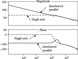
FIGURE 14.20 Bode plots for the boost converter case.
Circulation currents between power converters can appear if the switching pattern in one or more converter legs is different from one power stage to another. Assuming that only one phase shows a circulation current, the power converter’s three currents can be written as
Ia = × + sin(ωt), Ib= sin(ωt + 120), Ic = sin(ωt + 240)
After (a, b, c) transforms to (d, q), (0.66x) adds up to (d, q) components and (0.33x) adds up to the zero-sequence component.
It is important to note the integrative action of the zero sequence components. When a voltage is applied across the inter-phase inductors, owing to the different switching patterns in different power stages, the zero-sequence current increases or decreases depending on the polarity of the voltage. When a zero voltage is applied, the zero-sequence current is kept constant. Repetitive voltage across the inter-phase inductor can increase the zero-sequence component at values dangerous for the power stage.
In current control, the use of PI control on each of the (d, q) axes ideally withdraws the additional component (0.66x) on these axes and does not affect the component on the zero-sequence axis. All three phase currents are subjected to an equal amount of error. If this is too large, we need a zero-sequence controller.
The zero-sequence current is not seen in the common-mode model, as it is a part of the differential mode model. This means that a power system with N parallel converters needs only N − 1 controllers, as there are N − 1 independent currents. Each zero-sequence current controller is designed from the inter-phase inductances that appear on the zero sequence equivalent circuitry.
14.5 INTERLEAVED OPERATION OF POWER CONVERTERS
The same parallel-connected hardware can be operated in multiple ways leading to reduced ripple in the aggregate input and output waveforms (Figure 14.17). The simplest solution is to use the same PWM clock for all converters. The switching pattern results are identical and the whole power stage behaves like a single highpower converter.
Different power converters can use different clock signals producing IN/OUT current waveforms with a ripple reduced by √N owing to passive (stochastic) ripple cancelation. This is definitely not a practical solution. The existing hardware can be controlled with equal phase displacement (2π/N) producing the so-called interleaving (Figure 14.21). The ripple magnitude is reduced by N times and the ripple frequency is increased by N times, simplifying filtering. This solution was first used for DC/DC converters and it is increasingly used in AC applications. Buck or boost topologies have been interleaved for a long time to improve harmonics and to share power between several power devices. Advanced methods send the current sharing information through the harmonic content of these converters. This is mainly possible due to the large ratio between the switching frequency and the control bandwidth. In contrast, AC applications use lower switching frequency and the control bandwidth is limited.
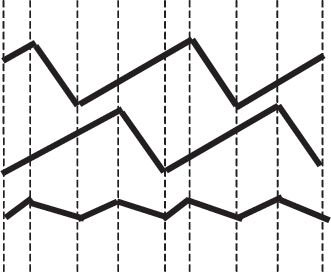
FIGURE 14.21 Ripple composition by interleaving.
Interleaving has been used for other classes of three-phase converters such as the buck-derived three-phase converters (in reference 7 of Chapter 3) (Figure 14.22a) or the B4 inverter modules (in reference 8 of Chapter 3) (Figure 14.22b). All these have given an extensive analysis of interleaved six-switch three-phase converters [6,9,10,12].
There are numerous advantages in using interleaving control of parallel hardware. The most important advantage is in using prior knowledge to build, control and protect the single-unit three-phase inverters and converters. Other advantages are discussed next (Figure 14.23).
The ripple of the sinusoidal phase current is maximum when the area under the curve of inductor voltage (volt seconds) or the phase voltage is maximum. Accordingly, the ripple of the current that results from interleaving is reduced. Both conduction losses and filter losses are minimized by interleaved operation of parallel hardware. Reliability is improved by parallel hardware and a good level of redundancy is ensured. Finally, parallel hardware ensures electronic gearing.
It has been shown that the circulating currents are the result of differences between the switching patterns within different power stages. The amount of the circulating current is influenced by the selection of the PWM algorithm in multiple modes.
First, the circulation currents depend on the difference between the reference waveforms (or ON-times) used on each power converter, as shown in Figure 14.24. In short, the sinusoidal PWM leads to the smaller difference between references and the smaller circulating current between power stages.
Another type of circulating current results from different active vectors used on each power stage. As a result of the use of different active vectors at the same time, one leg of the inverter is connected to the +DC bus, while the same leg on another inverter is connected at −DC bus. Such circulation current gets decomposed on (d, q, 0) components and can be partly corrected through the (d, q) current controllers.
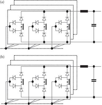
FIGURE 14.22 Different topologies used within interleaved configurations: (a) buck-derived three-phase cenverters. (b) B4-Inverters modules.
Finally, pure zero-sequence currents are produced when all three switches connected to one terminal of the DC bus are ON, while the three inverter poles on the other inverters are connected at the other terminal of the DC bus. This happens when one converter uses a zero vector and another converter uses the other possible zero vector. Special PWM methods can be employed to avoid using any zero vector (Figure 14.25).
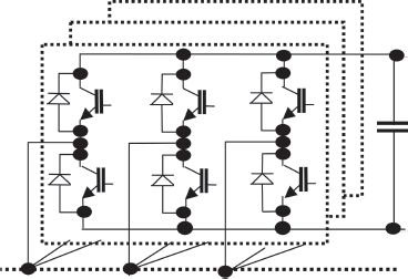
FIGURE 14.23 Circulating currents from differences in the PWM references.
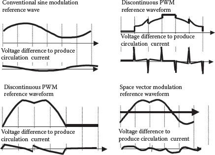
FIGURE 14.24 Different interleaving possibilities for an even number of converters. (From Neacsu, D.O., Wagner, E., Borowy, B. 2002. 37th IAS Annual Meeting. Conference Record of the Volume 3, 13–18 October, pp. 1958–1965. With permission.)
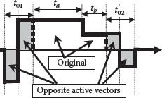
FIGURE 14.25 Generation of the PWM sequence without any zero vector.
An alternative solution is to select the same zero state in all power converters whenever a zero state is necessary. The selected common zero state can be changed in a few seconds to avoid temperature run-up. Using always the same zero vector, no matter what active vectors are employed during the PWM sampling interval eliminates the possibility of circulating currents associated to identical zero states.
14.7 SELECTION OF THE PWM ALGORITHM [1,2]
Previous chapters have presented different PWM algorithms to control a three-phase inverter. Interleaved control of parallel hardware can be based on any of these algorithms. We limit our analysis to carrier-based PWM (asymmetrical or symmetrical), SVM, discontinuous PWM implemented on the SVM support to minimize loss, or special PWM with the same zero state. Any of these methods can be generated by symmetrical (center-aligned) PWM or asymmetrical PWM depending on the state sequence at the switching interval. The type of PWM employed influences the harmonic content and waveform shapes of the phase currents, circulation currents, neutral voltage, and DC side currents.
When using symmetrical PWM on an even number of interleaved converters, there are two possibilities for selecting the most suitable switching sequence, and these are shown in Figure 14.26.
Extensive analysis has established comparative results that can be grouped into the following conclusions:
• General Remarks
• The first high-frequency components of the phase currents are always at Nfsw, where N is the number of interleaved power stages.
• The first high-frequency component of the zero-sequence current is always at fsw. The DC bus and the neutral voltages show the first component at Nfsw frequency, except for possible components owing to system asymmetries.
• Using PWM with an optimal sequence to reduce the load current harmonics produces more harmonics on the individual inverter currents.
• When circulating currents are reduced, the peak-to-peak neutral voltage bounces across a larger interval.
• Carrier PWM
• Symmetrical PWM produces less harmonics in the inverter currents than does asymmetrical PWM.
• Interleaving of symmetrical PWM can be implemented by pulse or by period (Figure 14.26).
• The zero-sequence currents in symmetrical methods are larger due to greater superposition of different states.
• Peak-to-peak neutral voltages are also lower for the symmetrical PWM methods.
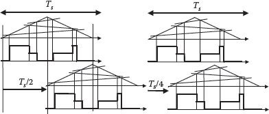
FIGURE 14.26 Different interleaving possibilities for an even number of converters.
• Reduced Loss PWM
• Reduced-loss PWM shows a very large zero-sequence current at a low frequency if no zero-sequence current controller is used.
• Zero-sequence controller becomes mandatory with SVM or reduced loss PWM algorithms.
The most important conclusion of this study is that using sinusoidal PWM algorithms in interleaved applications is more advantageous than SVM or Reduced-Loss PWM algorithms.
Each individual three-phase inverter is controlled by the same controller as in a single-unit application. PWM, power stage protection, and current control are implemented locally within each inverter’s control module (Figure 14.27).
References for these controllers are provided from a system controller. The main tasks for the system controller are the proper current distribution among inverters, tight output regulation, hierarchical protection, and user interface or control through a reference.
The most important task is to distribute current equally between power converters. This can be achieved with master-slave control, central-limit control, or circular-chain control [4,5,11] (Figures 14.28 and 14.29).
Ultimately, each of these methods has to have an effective communication protocol or interface. As local control is ensured with hardware controllers located at each power converter, each system controller must be equipped with at least two communication ports. The first communication port is needed to communicate between power stages to ensure current sharing and fault management [13]. The information sent over this communication channel depends on the selection of the system controller structure such as the master-slave control, central-limit control, and the circular-chain control.
The second channel is used for PC interfacing for online monitoring and development and it can be considered local.
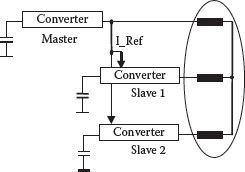
FIGURE 14.27 Parallel connection of six-switch three-phase converters.
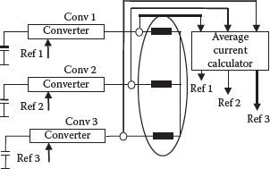
FIGURE 14.28 Master-slave structure.
Both required communication channels are bidirectional and a serial support is preferred owing to system complexity. Possible communication links for multiconverter applications are CAN, RS232, or RS485. The converter control S/H is strongly affected by the communication baudrate or bandwidth. To achieve a control S/H at each PWM cycle, the communication link should ensure a full exchange of information at the PWM frequency rate. This is a very serious constraint and limitation.
The last issue to be solved by the system controller is related to protection at a higher hierarchical level. It has been already shown that the local controller should ensure a fast protection of the power semiconductor devices, and shutdown quickly in case of overcurrent, IGBT desaturation, overvoltage, or overtemperature. These are faults that can occur quickly and require immediate attention. After a shutdown decision has been taken, the shutdown event information is processed by each converter controller and the software enters a special routine for shutdown and fault debouncing. The inter-converter network baudrate is limited and instant global decision is not possible. The solution considered often is to distribute faults depending on the required response time. Some faults are sent over the regular communication link and some are transmitted over an emergency hardware wire for a quick shutdown of all power converters. System monitoring is ensured through periodical status reports for the faults that do not require quick response action. A special software routine appraises the system and corrects existing faults on the basis of these reports. Definition of this software routine for start-up and/or coming back from the shutdown state is very important.
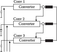
FIGURE 14.29 Circular chain control.
Another fault that could happen during operation is the loss of the communication link even temporarily. The most common solution uses a special communication protocol that has parity checking and security features for surveillance of the communication channel. This further reduces the communication baudrate. The special communication protocol sets a flag for the appropriate fault and the software algorithm initiates a shutdown procedure, otherwise uncontrollable circulating currents can occur within each converter. Local software can detect these faults and shutdown independently. Simplified solutions are often used instead of the special communication channel, by settling a fault bit within the regular fault message sent through the communication channel.
This chapter presents the details of the parallel and interleaved operation of parallel three-phase hardware. It is, therefore, demonstrated that interleaved operation of three-phase systems is a viable solution for medium and high power converters, especially in applications with low voltage and high current [14,15]. Design aspects and selection of the inter-phase reactors or PWM algorithms are also shown.
P14.1 |
A power electronic converter needs to parallel three F-series 600 V Powerex IGBTs to constitute each switch. What is the static derating factor that we should consider? |
P14.2 |
For the same power converter, if the IGBTs are 200 A devices, what is the maximum current this structure will allow through all three IGBTs? |
P14.3 |
Consider an interleaved power converter with two inverter power stages, each controlled with sinusoidal PWM at 10 kHz and operated at grid frequency of 60 Hz and delivering 120 V RMS in open loop. Calculate the low-frequency component applied permanently on the inter-phase inductors. What is the low-frequency circulation current if each inductor has 100 mH. |
P14.4 |
Consider the time constant equations of the SVM algorithm as given by Equation 5.30. Define the new time intervals corresponding to Figure 14.27. Draw the switching pattern within one sampling interval to generate a vector in the first sector. Is there any way by which this can be implemented in a center-aligned PWM-support hardware? |
1. Neacsu, D.O., Borowy, B., and Bonnice, W. 2001. Limiting inter-converter zero sequence currents within three-phase multi-converter power systems—Review and ultimate solution. IEEE IECON, Denver, CO, USA, pp. 1255–1261.
2. Neacsu, D.O., Wagner, E., and Borowy, B.N. 2002. Selection of the PWM algorithm for 3-phase interleaved converters. IEEE IAS, Pittsburgh, PA, USA, pp. 13–19.
3. Garg, A., Perreault, D.J., and Verghese, G.C. 1999. Feedback control of paralleled symmetric systems with applications to nonlinear dynamics of paralleled power converters. Proceedings of the 1999 IEEE International Symposium on Circuits and Systems, ISCAS ‘99, vol. 5, pp. 192–197, 30 May–2 June.
4. Zhou, X., Xu, P., and Lee, F.C. 2000. A novel current-sharing control technique for low-voltage high-current voltage regulator module applications. IEEE Trans. PE 15(6), 1153–1162.
5. Wu, T.F., Chen, Y.K., and Huang, Y.H. 2000. 3C strategy for inverters in parallel operation achieving an equal current distribution. IEEE Trans. IE 47(2), 273–281.
6. Perreault, D. and Kassakian, J. 1997. Distributed interleaving of paralleled power converters. IEEE Trans. CAS 44(8), 728–734.
7. Mazumder, S., Nayfeh, A., and Borojevic, D. 2002. Comparison of nonlinear and linear control schemes for independent stabilization of parallel multi-phase converters. IEEE IAS.
8. Mazumder, S.K., Nayfeh, A.H., and Borojevic, D. 2001. A novel approach to the stability analysis of boost power-factor-correction circuits. IEEE 32nd Annual Power Electronics Specialists Conference, PESC 2001, Vancouver, Canada, vol. 3, pp. 1719–1724, June.
9. Kelkar, S. and Henze, C.P. 2001. High performance three-phase unity power factor rectifier using interleaved buck-derived topology for high power battery charging applications. IEEE 32nd Annual Power Electronics Specialists Conference, PESC 2001, Vancouver, Canada, vol. 2, pp. 1013–1018, June.
10. Singh, B.N., Joos, G., and Jain, P. 2000. Interleaved 3-phase PWM AC/DC converters based on a 4-switch topology. IEEE 31st Annual Power Electronics Specialists Conference, 2000. PESC 2000, Galway, Ireland, vol. 2, pp. 1005–1011, 18–23 June.
11. Wu, T.F., Chen, Y.K., and Huang, Y.H. 2000. 3C strategy for inverters in parallel operation achieving an equal current distribution. IEEE Trans. IE 47(2), 273–281.
12. Chang, C. and Knights, M.A. 1995. Interleaving technique in distributed power conversion systems. IEEE Trans. CAS 42(5), 245–251.
13. Donescu, V. 2001. Fault detection and management system broadcasts motor drive faults. PCIM, June, 38–42.
14. Anon. 2000. FM2000—Modular drive design up to 2000HP. TECO-Westinghouse internet documentation.
15. Anon. 2000. Drive modules offer system integrator flexibility. ABBACS600 in Engineering Talk.
16. Neacsu, D.O., Wagner, E., Borowy, B., 2002. 37th IAS Annual Meeting. Conference Record of the Volume 3, 13–18 Oct. 2002, pp. 1958–1965.