
3.1 HIGH-POWER DEVICES OPERATED AS SIMPLE SWITCHES
Using semiconductor devices such as bipolar transistors and MOSFETs at somewhat higher power levels in the active region yields low efficiency. A voltage regulator built with a bipolar transistor working in the active region can barely provide an efficiency of 30–40% because of the large collector–emitter voltage drop. In contrast, operation of the same device in switch mode allows efficiencies of 80–99%, depending on the converter topology and the number of passive elements. The whole idea of using switches is to operate at high frequency with a constant or variable duty cycle followed by low-pass filtering with a passive filter. The DC or low-frequency component of the converter waveform is therefore derived and used as a result of the power transfer.
Take the example of a switch controlled to produce a voltage on the load (Figure 3.1). This is the simple case of a step-down DC/DC conversion. If a low-frequency AC component is injected in the duty cycle of the switch, a low-frequency variation is seen on the load (Figure 3.1). In other words, the low-frequency component of the load voltage reflects the control reference. Figure 3.2 illustrates this principle of modulating the pulse width (or duty cycle) of a buck (step-down) converter according to a variable control function.
Figure 3.2 also helps us to understand the difference in terminology between duty cycle and modulation index. The former characterizes the variation of the whole control reference, whereas the latter concerns the control of each individual switch. Therefore, we can modify the load voltage root mean square (RMS) on the fundamental frequency through the modulation index.
Many power loads are actually supplied in current, and the goal of power conversion is to provide a smooth variation in the load current. In such a case, the filtering task is partly laid on the inductive component in the load circuit, which is able to transform pulses of voltage into smooth current. If the load already has enough inductive components, it is not necessary to add an inductive filter in the system; the load itself will take care of the filtering task.
Conversion at higher power levels requires drawing power from a three-phase grid system and delivering it to a three-phase load. Special topologies have been developed for three-phase power conversion and their operation is more complex than a single switch-based DC/DC converter. Particularities within the operation of the three-phase power converter are presented in this chapter. The main power devices used today in building power converters have already been introduced in the previous chapter.
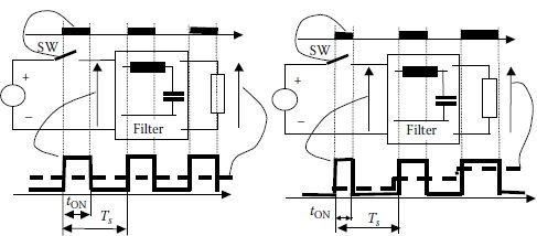
FIGURE 3.1 Basic switch operation: constant and variable duty cycle.
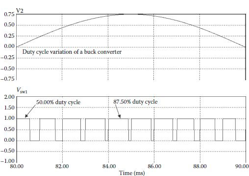
FIGURE 3.2 Duty cycle with an AC variation.
3.2 INVERTER LEG WITH INDUCTIVE LOAD OPERATION
The simplest circuit to produce an AC waveform on the output is shown in Figure 3.3.
To simplify our explanation, a pure inductive load is first considered. The high-side switch S1 and the low-side diode D1 constitute a buck converter during the positive half-wave of the inductor current. Analogously, the low-side switch S2 and the high-side diode D2 form a buck converter during the negative half-wave of the inductor current. During the ON-time of any switch (S1 or S2), energy is charged on the inductor depending on the width of the ON-time interval. Diodes (D1 or D2) ensure a circulation path for the currents during the OFF state of the switches. Overall, the current through the load inductor follows the control reference, with the delay given by the load power factor. Because of this phase-shift between the control reference and the actual load current, it becomes mandatory to control both switches in a complementary manner. If each switch is controlled on its appropriate buck converter half-wave, an interval without any switching of the load voltage will be necessary for inductor current to discharge through the diodes (Figure 3.4). A complementary control is shown in Figure 3.5. The load current is always under control and it follows a quasi-sinusoidal waveform with a constant phase-shift from the control reference.
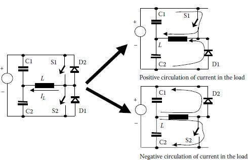
FIGURE 3.3 Current circulation for control of a converter leg.
Both cases presented in Figures 3.4 and 3.5 show a continuous variation of the width of voltage pulses applied to the load. This is called pulse width modulation (PWM). The modulating waveform coincides with the control waveform and pulses are produced at a constant frequency. The carrier pulses are ensured by a waveform called carrier signal. The way the modulating and carrier signals are produced and compared differentiates between PWM algorithms [10,11,12,13,14].
Figure 3.2 presents a very generic power converter. In practical applications, other topologies may be employed and the load might not be a simple inductance. The principle of transferring energy from a source in a switched operation mode ensuring high efficiency of the conversion always remains the same. It has already been shown that the controls for such operation are called PWM techniques.
In the AC/DC conversion case, it is obvious that the line or boost inductance acts as a low-pass filter (LPF) for the applied voltage. Considering an AC drive, the machine inductance filters the harmonics provided by the discontinuous power flow at switching. The flux linkage in the machine’s windings is approximately equal to the time integral of the impressed voltage, if a drop in voltage across resistance and leakage inductance of the stator windings are neglected. No matter how the inductance appears on the load circuit, the power transfer is ensured through PWM.
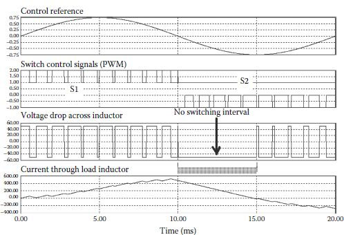
FIGURE 3.4 Control of each switch only on its appropriate half-wave (1 kHz switching frequency, 100 VDC, m = 0.75 and 0.5 mH inductor).
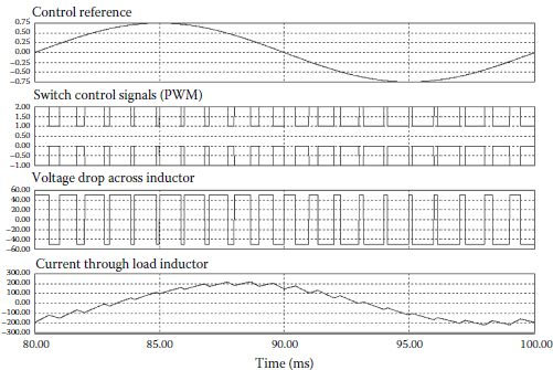
FIGURE 3.5 Control of each switch on the whole waveform (1 kHz switching frequency, 100 VDC, m = 0.75 and 0.5 mH inductor).
The great advantage of the PWM algorithm is its ability to control the content in fundamental voltage across the load. This is ensured by the modulation index that is related to the magnitude of the control reference waveform. For instance, the examples shown in Figures 3.4 and 3.5 are based on a modulation index of 0.75. The pulse width variations are based not only on the shape of the control reference but also on this modulation index. The pulse widths modify the charge and discharge intervals of the energy within the load inductor. Accordingly, the ripple of the current through load will depend on the variation of the pulse width. It is important to note that the duty cycle of the switch control coincides with the modulation index in the converter shown in Figure 3.2. Figure 3.6 shows how all waveforms depend on the modulation index. The load current ripple depends on the modulation index value.
Fourier or frequency analysis provides an instrument with which to compare the amount of ripple or harmonics that results from operating at one modulation index or another with one converter topology or another. Fast Fourier transform (FFT) results for the voltage applied to the load at different modulation indices and different switching frequencies are shown in Figures 3.7 and 3.8 for the converter shown in Figure 3.2.
If no modulation is involved, the harmonic spectrum of the output voltage shows a strong harmonic component at the switching frequency. When the modulation index increases, the component at the switching frequency decreases, and the low-frequency component at the frequency of the modulating signal increases. A part of the power transfers from the switching frequency component to the fundamental. The best case, with the most pure low-frequency component synthesis, is achieved at higher modulation indices. However, the modulation index can increase only until the wider pulse in the pattern fits the whole sampling (or switching) period interval. After this point, any increase of the modulation index will produce distortion of the synthesized fundamental frequency waveform.
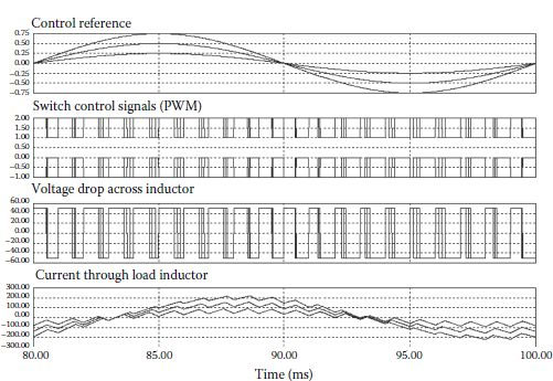
FIGURE 3.6 Waveforms characterizing the converter operation with different modulation indices.
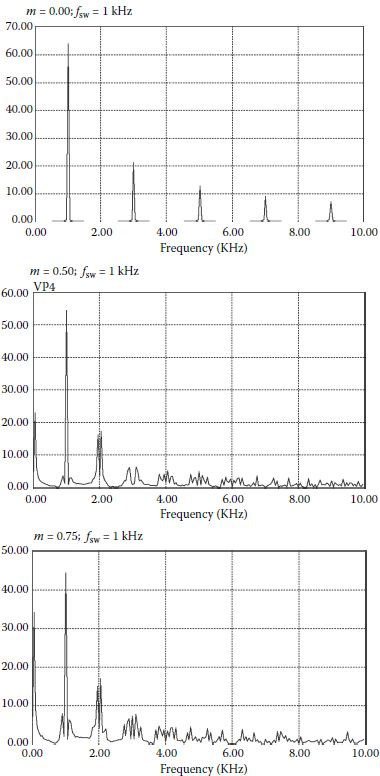
FIGURE 3.7 Output voltage spectra of different operation modes of the converter from Figure 3.2 at 1 kHz switching frequency.
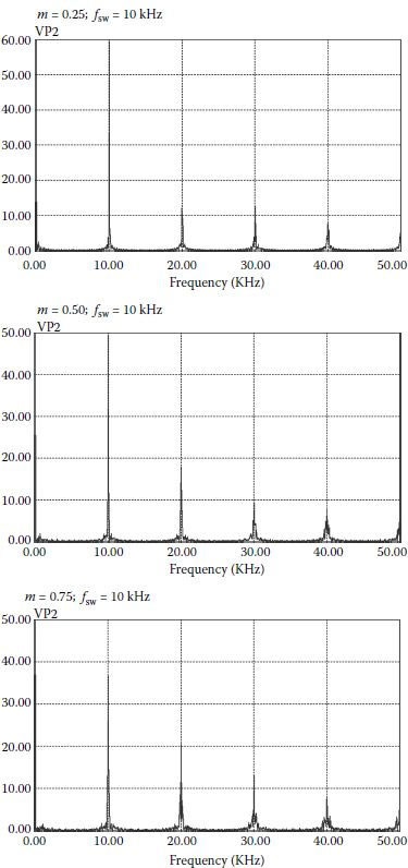
FIGURE 3.8 Spectra of different operation modes of the converter from Figure 3.2 (10 kHz).
Conclusions of these harmonic results can be grouped as follows:
• The main effect of modulation is to move the harmonics toward higher frequencies where they can be filtered easier.
• The load voltage spectra contain no DC component, but only components of fundamental frequency and multiplies of the switching frequency.
• The magnitude of the components at multiples of the switching frequency is smaller when frequency increases.
• More harmonics are observed at lower modulation indices.
Global harmonic performance coefficients provide a better comparative image. Section 3.8 makes a complete discussion of these coefficients.
3.4 BASIC THREE-PHASE VOLTAGE SOURCE INVERTER: OPERATION AND FUNCTIONS
Figure 3.2 has shown a possible solution for energy conversion from a DC power supply to a single-phase AC load. AC has been achieved on the load by PWM. At higher power levels, it is common to receive or deliver power on a three-phase system. Power is, therefore, distributed equally on the three phases, and the current in each phase is smaller.
The simplest solution to define a three-phase converter is to multiply the structure of Figure 3.2 on three similar circuits. Figure 3.9 shows such a converter. The operation of each inverter leg is identical to the operation of the converter from Figure 3.3 with reference voltages shifted 120° from one leg to another.
A star-connected three-phase load is represented in Figure 3.9. The load neutral point is connected to the mid-point of the capacitor bank. As the load voltages follow the three-phase reference system, the fundamental voltages applied to the load also form a three-phase system. If the load is symmetrical, the phase currents form a system with no zero sequence, which means that there is no current circulation from the load to the capacitor bank mid-point. The load can be disconnected from the capacitor bank mid-point and an alternative delta-connected load can also be considered (Figure 3.10). Because the phase currents must add up to zero, there is no zero-sequence in the currents for the star-connected load without connection to the DC capacitor bank mid-point.
It has been shown that switches have been controlled on each phase with sinusoidal references modulating the duty cycle of the pulses. The phase voltages can be expressed with dependence on the switch voltage drop.
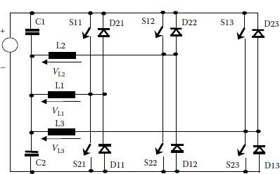
FIGURE 3.9 Three-phase inverter derived from the single-phase topology.
The main constraint for PWM generation is the need to produce a symmetrical set of voltages on the load (Figure 3.11). This can be expressed as
(3.1) |
The circuit equations are
{Vph A=Vpole A−VNOVph B=Vpole B−VNO⇒Vpole A+Vpole B+Vpole C=3VNO⇒VNO=13[Vpole A+Vpole B+Vpole C]Vph C=Vpole C−VNO |
(3.2) |
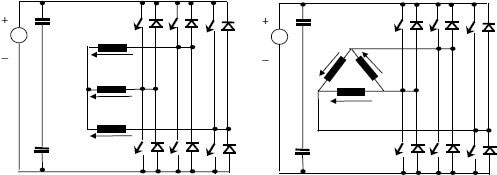
FIGURE 3.10 Different load connections.
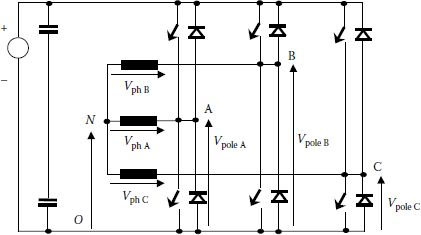
FIGURE 3.11 Voltage construction on the load.
These equations can be seen both in average and instantaneous values. The average analysis neglects all switching processes. If the pole voltages follow sinusoidal references superimposed to half of the DC voltage, the VNO voltage always equals half the DC voltage. If we consider a third or a multiple of the third harmonic injected identically within the pole voltages Vpole A, Vpole B, Vpole C, this harmonic will be found on the VNO voltage. Any shape of a repetitive signal on the third harmonic frequency will satisfy the same remark. Furthermore, as the same signal is a part of the pole voltages and the neutral voltage, it is not seen on the output phase voltage. This leads to a very important conclusion: third and multiple of three harmonics in the modulator reference voltages are not seen on the output phase voltages. It will be shown later that this conclusion helps increase the maximum modulation index.
The previous equations in instantaneous values help demonstrate that the phase voltages equal 1/3 VDC, 2/3 VDC, −1/3 VDC, −2/3 VDC, or 0. This also implies that the VNO voltage does not maintain a stiff constant DC voltage, but changes between different levels of voltage at each switching.
The operation of the ideal converter with a six-step modulation or PWM outlines the following conclusions for the output phase voltages:
• There is no even order harmonics
• There is no 3rd harmonic or harmonic multiple of three
• There is no DC component
Accordingly, a typical spectrum of the load voltage is characterized by fundamental, pairs of 6 k ± 1 order harmonics (5,7,11,13,17,19,…), up to the switching frequency and its multiplies. Examples of spectra of the load voltage are included in Figures 3.12, 3.13, 3.14. A low ratio between switching frequency and the frequency of the sinusoidal reference has been assumed in order to outline the lower-order harmonics.
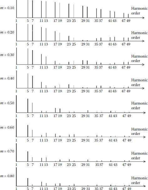
FIGURE 3.12 Six-step operation.
The six-step operation (without modulation) of the three-phase inverter produces large harmonics of the load voltages. Different methods for harmonic improvement have been introduced:
• Connection of several identical power stages through transformers and control with phase shift in order to add up voltage or current waveforms on the load (Figure 3.15)
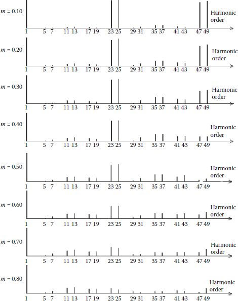
FIGURE 3.13 Switching frequency 24 times larger than the sinusoidal reference frequency.
• Control with PWM algorithms such as
• Programmed pattern calculated to optimize a harmonic coefficient for low-frequency range or for reduction of certain low-frequency harmonics
• Triangle-intersection or direct digital pulse-programming techniques to achieve carrier-based PWM methods (carrier-based PWM algorithms)
• Vectorial PWM methods
Each of these methods will be detailed later with specific examples of applications. Before pursuing such analysis, let us understand what the requirements are for performance indices in three-phase inverters.
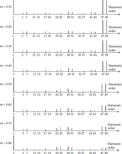
FIGURE 3.14 Switching frequency 48 times larger than the sinusoidal reference frequency.
3.5 PERFORMANCE INDICES: DEFINITIONS AND TERMS USED IN DIFFERENT COUNTRIES
In order to compare the results from different PWM methods and different power converters, several performance indices are defined based on frequency analysis. These analyses of the voltages and currents at the input or output of a power converter can be performed with coefficients of the Fourier series or with Fourier transform.
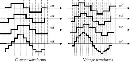
FIGURE 3.15 Harmonic improvement by adding-up voltage or current waveforms from individual power converters. Off-line optimization of the phase-shift is required.
Any periodic function can be developed in a constant value and an infinite series of sin and cos functions on even and odd multiples of the fundamental frequency.
This is called Fourier series and it is easy to apply for signals defined analytically.
u(ωt)=A02+A1 sin (ωt)+A2 sin (2ωt)+⋯+An sin (nωt)+⋯ +B1 cos (ωt)+B2 cos (2ωt)+⋯+Bn cos (nωt)+⋯ |
(3.3) |
where
(3.4) |
(3.5) |
(3.6) |
Components on the same frequency determine the magnitude of the respective harmonic.
(3.7) |
with the RMS value of
(3.8) |
Previous results shown in Figures 3.12, 3.13, 3.14 have used the Fourier series.
If the waveform is not defined analytically, but as a set of measurements or simulation results, then it is worthwhile to calculate the Fourier transform. This converts a time domain periodic function into a frequency domain function called spectral function.
(3.9) |
where nε (–∞,∞).
The reverse transform is given by
(3.10) |
Numeric calculus is achieved for an approximation of the Fourier integral when samples of the measured signal are known as u(kT) = uk. In this respect, let us consider T = NTs and dt = Ts.
(3.11) |
The sampling theorem states that N samples of a signal can define (N/2) – 1 positive spectral components and (N/2) – 1 negative spectral components. Function u(t) is periodic and this implies S(–nω) = S((N – n)ω). This further allows conversion of the negative spectral components into the upper range (N/2, N – 1) and calculation of N spectral components from the N samples of the waveform in time domain.
Computer calculation of the spectral function S(nω) can be done after evaluation of the expression:
w=e−j2π/N
It yields:
(3.12) |
The sequence of calculus can be reduced when considering the number of samples as a power of two. The outcome is also named FFT. For instance, choosing 1024 samples and the advantages of the FFT algorithm reduces the running time to only 1% of the time required for conventional Fourier transform calculation.
Because of the limited resolution of the Fourier transform methods, each component is shown for an interval adjacent with a triangular shape. The base of this triangle will be smaller for a finer sampling of the original signal and its magnitude will better approximate the magnitude of the frequency component. Previous results shown in Figures 3.7 and 3.8 have been determined with FFT.
3.5.2 MODULATION INDEX FOR THREE-PHASE CONVERTERS
For a three-phase inverter, performance indices are defined with respect to the modulation index
(3.13) |
Commonly used performance indices are introduced next. Calculated results are introduced as examples, but details on how these results have been achieved are overlooked in order to simplify the presentation. Precise differences in results from different PWM methods will be shown in Chapters 4 and 5.
3.5.3.1 Content in Fundamental (z)
It represents the ratio between the RMS value of the fundamental of the output phase voltage (VL1) and the RMS value of the output phase voltage (VL). It is used mostly in Europe.
3.5.3.2 Total Harmonic Distortion (THD) Coefficient
(3.14) |
Results of this coefficient depend on the number of harmonics considered in calculus. It is a good practice to consider a number of harmonics several times larger than the switching frequency.
Figure 3.16 shows THD for different switching frequencies when the modulation index varies between 0.1 and 0.8 and when calculus is performed for an extremely large number of samples. It is obvious that for the same modulation index, the results are approximately identical, no matter what the switching frequency when the frequency ratio is a multiple of six. This certifies that a PWM algorithm is just moving harmonics from lower frequency to higher frequency without altering the power delivered on the load.
3.5.3.3 Harmonic Current Factor (HCF)
As the inductive load is basically a low pass filter (LPF), the higher order current harmonics will be attenuated. The remaining spectrum of the current will be different from one PWM method to another and from one switching frequency to another. A coefficient regarding current harmonics would better define the performance of a PWM method. Such a coefficient is called HCF and it can be expressed also based on the voltage harmonics at the converter output:
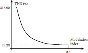
FIGURE 3.16 THD variation with the modulation index for 1.2; 2.4 and 3.6 kHz switching frequency when harmonics up to 150 kHz are considered.
HCF(%)=100I(1)√∞∑n=2[I(n)]2=100(V(1)/ωL)√∞∑n=5[V(n)nωL]2=100V(1)√∞∑n=5[V(n)n]2 |
(3.15) |
After some calculation, Figure 3.17 presents the HCF coefficient dependence on the modulation index for the three-phase converter shown in Figure 3.10. The larger the switching frequency, the lower the HCF coefficient.
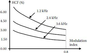
FIGURE 3.17 HCF variation with the modulation index for 1.2; 2.4 and 3.6 kHz switching frequency when harmonics up to 150 kHz are considered.
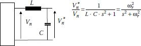
FIGURE 3.18 Output with filter of a power supply.
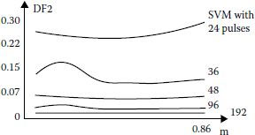
FIGURE 3.19 DF2 for regular SVM with different number of pulses on the fundamental period. (Adapted from Lucanu, M., Neacsu, D., and Donescu, V. 1995. Optimal Power Control Strategies for Space Vector PWM Inverters, Technical Bulletin of IPlasi, Romania, Tomme XLI (XLV), Fasc. 1–2, pp. 97–102.)
3.5.3.4 Current Distortion Factor
(3.16) |
This performance index is equivalent with HCF.
The requirements for AC power supplies consist of low output impedance and less than 5% voltage THD at load terminals. An output LC filter is necessary to decrease the THD content of the output voltage (Figure 3.18).
Let us note the harmonics of the filter output voltage V*n. Taking into account the effect of the filter and the transfer function between the filter output voltage and the inverter voltage, DF yields (Figure 3.19):
(3.17) |
3.6 DIRECT CALCULATION OF HARMONIC SPECTRUM FROM INVERTER WAVEFORMS
Any version of FFT can be calculated based on the samples of the waveform, but it requires extensive calculation. Calculation of the harmonic coefficients based on Fourier definitions is also complicated. This section introduces two methods for a quick estimation of the harmonic spectrum without integral calculation.
3.6.1 DECOMPOSITION IN QUASI-RECTANGULAR WAVEFORMS
Let us start with the quasi-rectangular waveform shown in Figure 3.20.
Applying Equation 3.5, the voltage harmonics can be expressed as
(3.18) |
All waveforms in power converters can be characterized with rectangular shapes. Moreover, such waveforms can be decomposed in periodic elementary quasi-rectangular waveforms, as shown in Figure 3.20. This approach can be applied to all staircase, two-level, and three-level waveforms.
Figure 3.21 shows the decomposition of a staircase waveform in quasi-rectangular waveforms.
Each harmonic component can be calculated by simple addition of the harmonics of the same order from the individual quasi-rectangular waveforms. The previous Fourier series development helps in the calculation of harmonics through simple addition.
(3.19) |
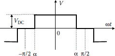
FIGURE 3.20 Waveform with parameter α.
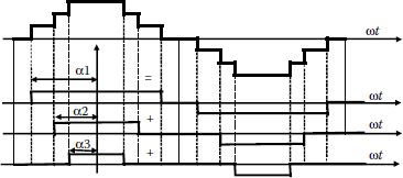
FIGURE 3.21 Decomposition in quasi-rectangular waveforms.
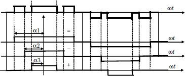
FIGURE 3.22 Decomposition of a PWM waveform.
Similarly, a PWM waveform can be decomposed into an algebraic sum of components (Figure 3.22).
The mathematical form of this decomposition is:
(3.20) |
Any periodic waveform can be decomposed into simple periodic rectangular waveforms with the same shape but phase shifted. The Fourier series of each such simple waveform is well known. Moreover, each harmonic component can be represented with a vector. Figure 3.23 shows an example of the waveform composed of simple square-waves. Adding up the appropriate waveforms is equivalent to adding up their corresponding vectors for fundamental frequency and generic harmonics of order n.
Simple mathematical relationships can be written for this vectorial composition. The magnitude and phase of a vector that results from composing two other vectors is well defined in mathematics textbooks. Definitely, this method is appealing for a reduced number of square-waves in decomposition.
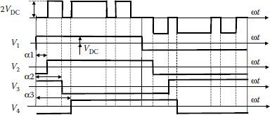
FIGURE 3.23 Decomposition in simple square-waves: (a) fundamental frequency; (b) n-th harmonics.
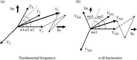
FIGURE 3.24 Vectorial composition.
The magnitude of the nth harmonics in the development of Fourier series for each individual square wave is provided by
Vn={4VDCnπ, for n=1,5,9,…−4VDCnπ, for n=3,7,11,…=(−1)k4VDC(2k+1)π, for k=0,…,∞ |
(3.21) |
The vectorial result can be computed easily by the decomposition of each particular vector on the real and imaginary axes, followed by algebraic operations on each of these two axes (Figure 3.24). It yields:
Re:VAll, Re 2k+1=V12k+1cosα1+V22k+1cosα2+V32k+1cosα3+⋯Im:VAll, Im(2k+1)=V12k+1sin α1+V22k+1sin α2+V32k+1 sin α3+⋯+Vn2k+1sin αn+⋯ |
(3.22) |
3.7 PREPROGRAMMED PWM FOR THREE-PHASE INVERTERS
The application of PWM methods in different industrial systems aims to improve global harmonic factors, reduce losses in the power converter or load, reduce torque pulsations in the motor drive applications, and reduce noise and vibrations.
It is easy to imagine a direct method of achieving this by optimal off-line definition of the switching instants. Results from all possible optimization criteria have reduction of low harmonics in common. This PWM can therefore operate without a fixed frequency but according to a preprogrammed pattern. The drawback of this approach is extensive computing. In comparison with carrier-based PWM or vectorial PWM, preprogrammed PWM can offer:
• Reduction of the inverter switching frequency by about 50%
• Direct operation into overmodulation providing more output voltage
• Reduced ripple of the DC current and elimination of the possibility of oscillations within the output filter
• Simpler implementation from a memory look-up table
3.7.1 PREPROGRAMMED PWM FOR SINGLE-PHASE INVERTER
Different topologies for single-phase voltage generation can be operated with bipolar PWM (two-level) or unipolar PWM (three-level) (Figure 3.25) [7,8,14,15]. The bipolar waveform can also be mathematically derived as a difference between a unipolar PWM and a square wave of half the amplitude. The following harmonic analysis supposes that waveforms are synchronized with a cos function and the Bn term equals zero.
The Fourier series for the three-level (unipolar) PWM can be expressed as
An=1n4VDCπ[∑Nk=1(−1)k−1 cos (kαk)]=1n[∑Nk=1(−1)k−1 cos (kαk)] |
(3.23) |
A DC bus voltage of π/4 has been considered for normalization in order to simplify calculation. The fundamental component can therefore be expressed as
(3.24) |
The first optimization constraint consists in setting a desired level of the fundamental. Canceling the 3rd, 5th, 7th, 9th, 11th, … harmonics require the appropriate Fourier coefficients to be zero. The number of degrees of freedom is provided by the number of angular coordinates αk. For instance, controlling the fundamental and cancelation of the first five odd harmonics is achieved when the output voltage has six level changes within a 90° interval.
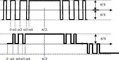
FIGURE 3.25 Bipolar and unipolar PWM waveforms.
If only cancelation of the first five harmonics is our goal, the following can be written:
A3=13[∑5k=1(−1)k−1 cos (3αk)]=0A5=15[∑5k=1(−1)k−1 cos (5αk)]=0A7=17[∑5k=1(−1)k−1 cos (7αk)]=0A9=19[∑5k=1(−1)k−1 cos (9αk)]=0A11=111[∑5k=1(−1)k−1 cos (11αk)]=0 |
(3.25) |
Solving this system yields the following values:
(3.26) |
Replacing these values for the fundamental component yields:
A1=cos(18.17)−cos(26.64)+cos(36.87)−cos(52.90)+cos(56.69)=0.74 |
(3.27) |
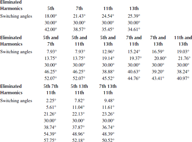
A proper adjustment of the VDC voltage can modify the content in fundamental A1. Similar calculus can be performed for any other harmonic condition (Table 3.1).
The bipolar (two-level) PWM wave has the following development in the Fourier series:
(3.28) |
A similar system of equations can be written for specific harmonic elimination or fundamental component control. For instance, elimination of the 5th and 7th harmonics along with the control of fundamental needs three angular variables.
TABLE 3.1
Eliminated Harmonics without Restriction on the Fundamental Content and the Appropriate Switching Angles
The equations yield:
A1=[−1+2( cos α1− cos α2+ cos α3)]=VA5=[−1+2( cos (5α1)− cos (5α2)+ cos (5α3))]=0A7=[−1+2( cos (7α1)− cos (7α2)+ cos (7α3))]=0 |
(3.29) |
As these equations are similar to those from the three-phase inverter analysis, a practical result will be shown later for the more popular case of a three-phase inverter.
3.7.2 PREPROGRAMMED PWM FOR THREE-PHASE INVERTER
For a three-phase voltage source inverter, elimination of low harmonics in the pole voltage (switching function) implies elimination of low harmonics in the phase voltage.
The harmonics in the line-to-line voltage (VLL) are related to the harmonics in the phase voltage through the following relationship:
(3.30) |
=1n∑n [cos (nαk)− cos n(αk+π3−π)]=1n∑n [cos (nαk)− cos n(αk+π3)]=1n∑n [2 cos n (αk+π6)− cos n(π6)] |
(3.31) |
The Fourier coefficients of the line-to-line voltage can be expressed by
(3.32) |
that is identical with the Fourier series for the unipolar PWM in the single-phase case.
However, symmetries for a three-phase system should be taken into account. Because of these symmetries, the switching-pattern calculation can be reduced to 30°. The three-phase switching pattern optimally defined for a 30° interval can then be used in the definition of the whole switching pattern. Switching instants within the first 30° interval are defined by an angular coordinate α measured from the beginning of the interval. Optimization can be set up based on appropriate waveforms for the phase voltages, VLL, or pole voltages in a three-phase voltage source inverter and for the phase currents within a current source three-phase inverter.
Similarly, operation of a single-phase preprogrammed PWM needs a pattern definition for 90°.
Therefore, it can be demonstrated that voltage reversals within the first 60° need mirror symmetries around the middle point situated at 30° from the beginning. For instance, a voltage transition from 0 to VDC at α1 implies a voltage transition from VDC to 0 at 60 – α1. Next, there should be no switching at the top of the waveform for a 60° interval (between 60° and 120° from the beginning of the waveform). The symmetry on the second harmonic imposes transitions on the following 60° with the same angular delays as on the first 60° interval. If all these conditions are respected, one can analyze only a single-phase waveform and account automatically for the cancelation of the second and third harmonics.
If the considered pattern has N switching instants within a 30° sector, N variables can be defined. For a given content in fundamental (A1), there are N – 1 degrees of freedom for harmonic elimination. The nonlinear form of these constraints provides the complexity of the optimization calculus.
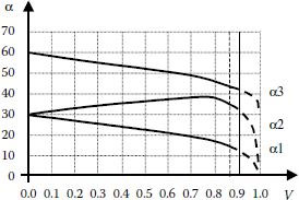
FIGURE 3.26 Solution for 5th and 7th harmonics eliminated with control of fundamental.
(3.33) |
where 2 M is the number of switching instants over a 30° interval and V is the desired fundamental voltage (current). Solving this system provides a set of values for αk at each V. Accordingly, the solution of Equation 3.27 or 3.33 can be presented graphically, as in Figure 3.26. Possible shapes of waveforms within a three-phase system are displayed in Figure 3.27.
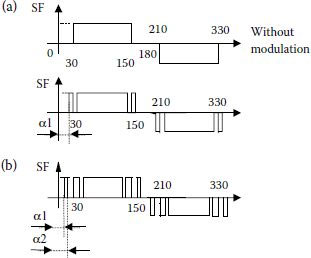
FIGURE 3.27 Examples of line-to-line voltage with eliminated harmonics.
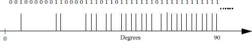
FIGURE 3.28 Binary programmed PWM.
This section presented methods for cancelation of specific harmonics. Other optimization criteria can be considered for minimization of THD, HCF, or torque harmonics [18]. They will lead to more complex calculus and require extensive use of computer programs, as MATHCAD or MATHEMATICA.
3.7.3 BINARY-PROGRAMMED PWM [1]
A version of the harmonic elimination principle can be achieved for a three-phase system with a division of the 30° interval in a fixed number of equal intervals. A variable is inserted at each of these sampling instants and optimization calculus is performed to define positive or zero values for these variables. Using symmetry, the whole waveform is finally built-up in the microcontroller memory.
For instance, Figure 3.28 applies this principle to a single-phase system required to cancel all harmonics up to the 13th and to maximize the content in fundamental [1]. The switching waveform results for 45 samples over an interval of 90° and the remaining higher harmonics are below 0.45% of fundamental. If applied to an induction machine, the torque harmonics result is below 3% of torque fundamental component.
3.8 MODELING A THREE-PHASE INVERTER WITH SWITCHING FUNCTIONS
Understanding the operation of each single-phase circuitry (Figure 3.3) helps define the controller for the three-phase converter. A very good tool for mathematical modeling of the operation of a three-phase converter is based on the switching functions concept. Given the repetitive manner of switching power devices within the three-phase power converter, one can define switching functions as periodical functions built up of rectangular pulses. The switching functions can commute within a limited number of states. This mathematical representation is possible only when switching of the power devices is not dictated by circuit operation (as in the SCR).
A conventional analysis of the converter presented in Figure 3.10 would need 36 circuit equations to be written for all currents and voltages. This system of equations can be further reduced to three if symmetries of the three-phase circuitry are considered. To simplify the mathematical model, switching functions are introduced. The definitions of the switching functions are not unique [2,3,4]. Let us consider several examples:
f1={1, S11 = on and S21=off0, S11 = off and S21=onf2={1, S12= on and S22=off0, S12 = off and S22=onf3={1, S13 = on and S23=off0, S13 = off and S23=on |
(3.34) |
Load voltages can be expressed with dependency on these switching functions:
(3.35) |
The DC current can also be calculated based on these functions:
(3.36) |
Another possibility:
Load voltages can now be expressed as
(3.38) |
The DC current can also be calculated on the basis of these functions:
(3.39) |
This method provides a mathematical relationship between the PWM control algorithm and the load voltages and DC current in a three-phase converter. Simulation tools can be built-up based on this concept, and they can provide a quick simulation without taking into account all the transient details pertaining to any peculiar power device. For instance, a direct implementation of these equations can be made in MATLAB-SIMULINK [2] environment, whereas an implementation with current and voltage sources can be accomplished in PSPICE [3].
3.9 BRAKING LEG IN POWER CONVERTERS FOR MOTOR DRIVES
Motor drives represent the greatest application for three-phase inverters. Power converters are manufactured especially for this application in the topology with six switches, presented in Figure 3.10. The braking deceleration of these motors transfers power to the intermediary circuit of these power converters. The basic requirements for a braking module have been analyzed in the introductory chapter. The DC voltage rises until the frequency converter trips for protection and it requires, sometimes, a special brake module to absorb this braking power. For power levels above 6.8 kW and less than 20 kW, the power converter itself includes an internal brake circuit and can accept an external brake resistor [4,7]. This resistor should be mounted on a heatsink and covered. For higher power levels, such braking modules can be attached outside [19].
This circuit is useful for dynamic regeneration during power dissipation, avoiding overcharging of the DC capacitor. This circuit is not rated for a continuously overhauling load, but it needs to absorb the peak brake power during large dynamics. It is rated for the average power calculated over a complete cycle.
(3.40) |
(3.41) |
where J is total inertia (kg m2); n1 the initial speed (RPM); n2 the final speed (RPM); tb the brake time (s); tc the cycle time (s).
A minimum value of the brake resistor must be defined to limit its current and power.
Then, we derate this calculus based on the ambient temperature at the moment of braking (Figure 3.29).
Another way to brake a motor is to use the DC brake. A DC voltage is applied across two motor phases to produce a stationary magnetic field in the stator. The braking power remains in the motor, which may overheat. For this reason, this method is used only in low-speed ranges.
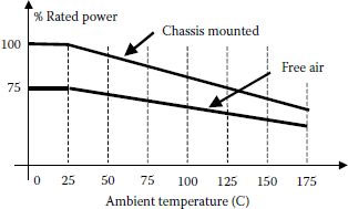
FIGURE 3.29 Derating based on temperature.
3.10 DC BUS CAPACITOR WITHIN AN AC/DC/AC POWER CONVERTER
The introductory chapter showed the role and features of the DC capacitor bank. The selection of the bus capacitors and the associated ripple aspects are next discussed. One of the functions of the DC capacitive bank is to reduce ripple. The input current to a three-phase inverter is composed of current pulses according to the switching sequence. An example is shown in Figure 3.30. The average value of these pulses represents the active power delivered to the three-phase inverter. The other harmonics compose the ripple to be filtered by the capacitor bank [5,6,16,17].
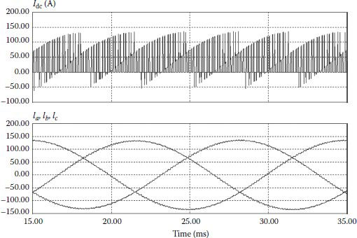
FIGURE 3.30 DC current and the phase currents of a three-phase inverter.
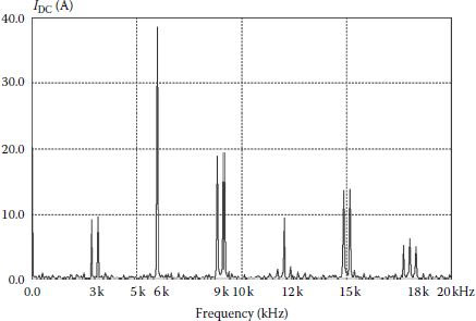
FIGURE 3.31 Spectrum of the DC current for carrier sinusoidal modulation at 3 kHz.
Aluminum electrolytic capacitors are usually selected in order to filter the front-end rectification waveform and to store the energy necessary for the dynamics of the load (Figure 3.31). This type of capacitor has an anode foil with an aluminum oxide layer acting as the dielectric, a cathode foil with no oxidation process, and a separator paper. All of them are wound together and impregnated with an electrolyte.
The equivalent circuit of an aluminum electrolytic capacitor is shown in Figure 3.32. The most important parameter is definitely the capacitance, and it is expressed by [5]
(3.42) |
where ε, is the dielectric constant, S the surface area of dielectric (cm2), d the thickness of the dielectric (cm). The dielectric constant is [8,9,10] within any aluminum electrolytic capacitor, whereas the dielectric layer is very thin, in the range of about 15 A per volt. The surface area is increased by electrochemically etching the aluminum foil up to 100 times in low-voltage foil and 25 times in high-voltage foil. This is the major advantage of aluminum capacitors, as they provide a larger capacitance when compared with other types of electrolytic capacitors.
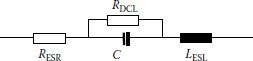
FIGURE 3.32 Equivalent circuit for an electrolytic capacitor.
The equivalent series resistance (ESR) represents the resistance that produces heat in the capacitor when the AC ripple current is applied. It is a combination of the resistive losses because of aluminum oxide thickness, electrolytic spacer combination, and resistance due to materials and material characteristics, such as foil length, tabbing, lead wires, and contact resistance.
The leakage current (DCL) corresponds to the DC current leaking through the capacitor. Ideally, it is well known that the capacitor is supposed not to allow any circulation of a DC current. However, small leakage of current occurs; it is proportional with capacitance and decreases when the applied voltage reduces.
The inductance of a capacitor (equivalent series inductance—ESL) is a constant and it depends on the mechanical mounting of terminals. The ESL is in the range of 3–40 nF and it influences the capacitor operation only at very high frequencies.
All these components contribute to the capacitor impedance. The frequency characteristic of this impedance has usually a notch in tens of kilohertz range, whereas the magnitude at lower and higher frequencies is higher. The lowest impedance value corresponds to the resonant frequency that turns the electrolytic capacitor into an inductor [6]. The frequency components within this frequency range will not be filtered by the electrolytic capacitor. Therefore, small low-inductance film capacitors (polyester or polypropylene) are generally used in differential or common mode to compensate the frequency characteristic of the electrolytic capacitor. A simple solution consists of using parallel connections with electrolytic capacitors in order to filter the harmonic components from current ripple and electromagnetic inference. The use of high-frequency film capacitors as DC bus snubber is suggested at the electrolytic capacitor terminals to minimize the connection inductance.
Finally, let us note two other important parameters in the selection of the DC bus electrolytic capacitor: the rated voltage and the ripple current. The rated voltage is calculated as the sum of the DC and AC voltages applied to the capacitor. If the ripple current is larger than a specified value, the life of the capacitor becomes shorter because of the heat generated by the excessive ripple current. Accordingly, there is an inverse relationship between the current ripple and the capacitor’s ESR.
This chapter introduces the single-phase and three-phase inverters and explains the challenges in meeting harmonic performance requirements. Details of preprogrammed PWMs are provided along with mathematical tools to calculate harmonics. Among all possible algorithms, the most used are the carrier-based PWM and the vectorial PWM that are explained in later chapters.
Finally, the brake leg and the DC capacitor bank are shown as possible auxiliary components of a three-phase inverter. Chapter 6 will provide the details on protection and building a three-phase inverter for different power levels.
P3.1 |
Figure 3.16 shows no difference between the THD of the output voltage for different switching frequencies at any modulation index. How can this be explained? |
P3.2 |
Consider Figure 3.21 with a DC voltage of 100 V. Write the mathematical constraints for achieving a fundamental voltage of 48 V and cancelation of the third and fifth harmonics (use Equation 3.19). Solve this system of equations and look for a solution with α1 < α2 < α3. |
P3.3 |
Consider Figure 3.22 with a DC voltage of 100 V. Write the mathematical constraints for achieving a fundamental voltage of 48 V and cancelation of the fifth and seventh harmonics (use Equation 3.20). Solve this system of equations and look for a solution with α1 < α2 < α3 < 30°. This condition also ensures that third harmonic vanishes. |
P3.4 |
Write Equation 3.22 for the case of Figure 3.23. Consider α1 = 12, α2 = 18, α3 = 23, and calculate the first seven harmonics. |
P3.5 |
Consider V = 0.4 and read α1, α2, α3 from Figure 3.26. Calculate the first 10 harmonics using these values in Equation 3.27. |
P3.6 |
Imagine a new definition of the switching functions for a three-phase inverter and write the appropriate dependency of the phase voltages and DC current on these switching functions. |
1. Said, W. 1989. Torque pulsations harmonics in PWM inverter induction motor drives. etzArchiv 11, 267–269.
2. Neacsu, D., Yao, Z., and Rajagopalan, V. 1995. Switching Function Analysis of Power Converters in MATLAB. Research Report, UQTR, Canada.
3. Salazar, L. and Joos, G. 1995. PSPICE simulation of three-phase inverters by means of switching functions. IEEE Trans. Power Electron. 9(1), 35–42.
4. Mohan, N., Undeland, T., and Robbins, W. 2002. Power Electronics, 3rd edition. John Wiley and Sons, New York.
5. Anon. 2000. United Chemicon Catalog H9.
6. Lai, J.S., Kouns, J.S., and Bond, J. 2002. A low-inductance DC bus capacitor for high-power traction motor drive inverter. IEEE Industry Applications Annual Meeting, 2002, Vol. 2, pp. 826–831.
7. Thornborg, K. 1988. Power Electronics. Prentice Hall, London, UK.
8. Brichant, F. 1984. Force-Commutated Inverters—Design and Industrial Applications. MacMillan Publishing Company, New York, USA.
9. Alex, D., Turic, L., and Stiurca, D. 1985. Umrichtersystem mit hoherem grundschwingungsge-halt fur die Drehstromtraktion. Bulletin SEV/VSE, Zurich, Switzerland, pp. 490–492.
10. Holtz, J. 1992. Pulsewidth modulation—A survey. IEEE Trans. IE 39, 410–420.
11. Holtz, J. 1994. Pulsewidth modulation for electronic power conversion. Proc. IEEE 82, 1194–1212.
12. Buja, G.S. and Indri, G.B. 1977. Optimal PWM for feeding AC motors. IEEE Trans. IA 13, 38–44.
13. Patel, H.S. and Hoft, R.G. 1973. Generalized technique of harmonic elimination and voltage control in thyristor inverters. IEEE Trans. Ind. Appl. 9, 310–317.
14. Neacsu, D. 2001. Space Vector Modulation. IEEE IECON Tutorial.
15. Enjeti, P., Ziogas, P., and Lindsay, J. 1990. Programmed PWM techniques to eliminate harmonics: A critical evaluation. IEEE Trans. IA 26, 302–316.
16. Enjeti, P. and Shireen, W. 1990. A new technique to reject DC-link voltage ripple for inverters operating on programmed PWM Waveforms. IEEE PESC 705–711.
17. Dahono, P.A., Sato, Y., and Kataoka, T. 1995. Analysis and minimization of ripple components of input current and Voltage of PWM Inverter. IEEE IAS Annual Meeting 3, 2444–2450.
18. Sun, J., Beineke, S., and Grotstollen, H. 1994. DSP-based real-time harmonic elimination of PWM inverters. IEEE PESC 679–685.
19. Anon. 2001. Drives 101—Lessons. and Danfoss Internet documentation.
20. Lucanu, M., Neacsu, D., and Donescu, V. 1995. Optimal Power Control Strategies for Space Vector PWM Inverters, Technical Bulletin of IPlasi, Romania, Tomme XLI (XLV), Fasc. 1–2, pp. 97–102.