
4.1 CARRIER-BASED PULSE WIDTH MODULATION ALGORITHMS: HISTORICAL IMPORTANCE
Figure 3.2 shows the principle of pulse width modulation (PWM) control, but it does not provide any information on how we can produce the modulation within a real hardware circuitry. In order to keep the pulse frequency constant, a carrier signal is necessary. Switches change their conduction states at moments of time that are determined by the intersections between our reference voltage and a triangular high-frequency signal with a fixed magnitude equal to unity. This operation is shown in Figure 4.1.
The frequency of the pulses is kept constant while their duty cycle is modulated. This is known as natural sampling, suboscillation or the subcycle method. The method and the names are derived from the initial hardware implementation. In the 1970s, when engineers were already using power semiconductor switches fast enough to support modulation, the only control hardware available was analog circuitry. It was therefore easy to generate the carrier signal as a triangular waveform and to achieve modulation by comparison with a variable reference.
The method described in Figure 4.1 allows several possible shapes for the triangular waveform (Figure 4.2):
• Center-aligned (a)
• Left-aligned (c)
• Right-aligned (b)
Secondly, the ratio (q) between the frequency of the carrier and the frequency of the reference signal can have different values. If q is small, harmonics can be improved if the following are taken into account:
• q should be an integer in order to have synchronous waveforms leading to a periodical train of pulses.
• q should be odd in order to produce the same number of pulses on both positive and negative half-waves. The output voltage, therefore, contains no even harmonics.
• The harmonic of order q is the dominant one.
• In a three-phase system, the third and multiple-of-three harmonics vanish when q is selected as a multiple of three.
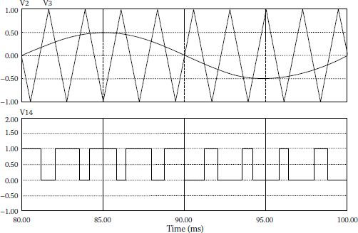
FIGURE 4.1 Sinusoidal PWM based on intersection between a triangular carrier signal and the reference.
The modulation signals could also have other shapes, such as trapezoidal and staircase (Figure 4.3), which provide advantages in the hardware implementation of the controller and in optimal switching performance at the power stage [1,2,3,4,5,6,7].
Finally, let us note here the advantage of a uniform-sampled PWM in digital implementation. This method samples and holds the sinusoidal reference at the same frequency as the carrier. The resulting reference looks like a staircase wave-form with elementary steps equaling the width of the carrier period. Figure 4.4 illustrates this method for a low-frequency carrier. Control pulses are obtained at the intersection of the S/H signal and the triangular waveform. A proper synchronization of these signals produces symmetrical signals.
A mathematical description of the harmonics of these carrier-based methods is difficult because the intersection moments are not linearly or equally spread over the reference cycle. Harmonics can be observed by FFT applied to simulation or measured data (Figure 4.2, right). The best harmonic content is achieved for the center-aligned pulses.
The case of a three-phase system can be treated as three individual modulators (Figure 4.5) with a star connected load. This load connection modifies the shape of the load voltage in each phase. Since the ratio of the switching and fundamental frequencies is chosen as a multiple of three (denoted with 6 k), high-frequency harmonics are seen in pairs at orders of 6 k ± 1. Frequency components at multiples of the switching frequency vanish.
Center-aligned PWM is also known as symmetrical PWM, whereas the left- and right-aligned methods are called asymmetrical PWM. Figure 4.2 showed the single-phase generation for each of these methods. The three-phase converter uses the same modulators, but the special load-connection modifies the shape of the load voltage and its spectrum.
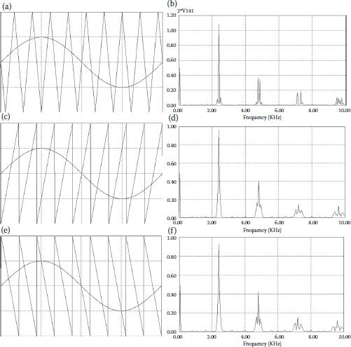
FIGURE 4.2 Different shapes of the triangular signal for q = 9 and modulation index of 0.5, for a single-phase inverter switched at 2.4 kHz: (a) time-domain waveforms for center-aligned triangular carrier; (b) spectrum of output voltage with modulation defined in (a); (c) time-domain waveforms for right-aligned triangular carrier; (d) spectrum of output voltage with modulation defined at (c); (e) time-domain waveforms for left-aligned triangular carrier; (f) spectrum of output voltage with modulation defined at (e).
4.2 CARRIER-BASED PWM ALGORITHMS WITH IMPROVED REFERENCE
The magnitude of the sinusoidal reference can be extended up to the magnitude of the carrier waveform. This situation corresponds to a maximum modulation index:
(4.1) |
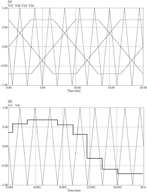
FIGURE 4.3 Trapezoidal and staircase references.
This is less than what is obviously possible when the pole (leg) voltage bounces on the full DC bus. This deficiency—of limited modulation index—is corrected by modified reference waveforms.
In Section 3.4, we have seen that a three-phase inverter can have third or higher order harmonics on the pole voltage without seeing them on the load voltage. Generally, any zero-sequence waveform can be added to the reference without being noticed on the load. This feature is used in applications that limit the peak-to-peak voltage applied to the load while preserving a high content in fundamental for this voltage. There is an infinite number of possible additions to the reference waveform that satisfy this condition.
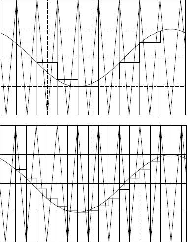
FIGURE 4.4 Uniform sampling of the reference signals.
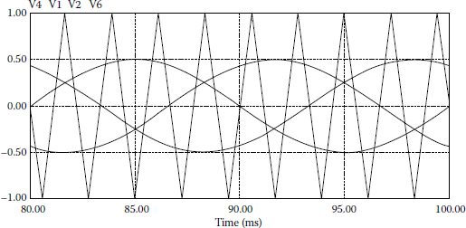
FIGURE 4.5 PWM generation in a three-phase system.
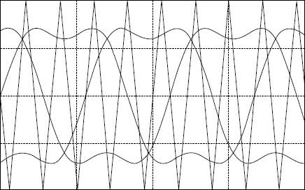
FIGURE 4.6 Injection of the third harmonic in the reference signal.
First, let us consider a simple third-harmonic injection with the phase selected to suppress the peak of the sinusoidal reference (Figure 4.6).
{vref, A=Vsin(ωt)+kVsin(3ωt)vref, B=Vsin(ωt+120)+kVsin(3ωt)vref, C=Vsin(ωt+2400)+kVsin(3ωt) |
(4.2) |
Considering k as a parameter, we can define the amount of the third harmonic to be injected in the reference signals in order to optimize performance indices such as maximum content in fundamental or minimum harmonic current factor (HCF) coefficient.
In [1], a minimization of the total harmonic distortion (THD) is considered and k = 1/4 is found as the optimal solution. Separate works [2,3] demonstrate that a third harmonic with k = 1/3 maximizes the fundamental voltage.
As the shape of the pole voltage is different from the shape of the phase voltage (Section 3.4), it is possible to keep one inverter leg unswitched and to produce the load three-phase system of sinusoidal waveforms out of the other two phases. Due to symmetries within a three-phase system, each interval of no switching can last for 60°. Accordingly, the reference function needs to be defined by six sets of functions, each one valid for 60°. A 50% theoretical switching loss reduction is therefore possible by not switching each switch for 60°. This opportunity was first explored in [4,5] and it was shown that discontinuous references produced by discontinuous zero sequence components can extend linearity above 0.785 up to the six-step operation fundamental and reduce switching losses. Later, other researchers proposed other shapes (or functions) for the zero sequence component. Figure 4.7 provides several examples [8,9,10,11,12,13,14,15].
The difference between these methods is the way in which we have selected the 60° interval when an inverter leg is not switched. It is advantageous to select between these methods based on each application and taking into account that switching losses strongly depend on the current through the insulated gate bipolar transistors (IGBTs). Power converters working on the grid application would benefit by using the first method in which the no-switching interval is produced around the peak of the voltage reference and phase current. Motor drive applications are typically characterized by a lagging current and the second method would be better, as it has the no-switching interval after the peak of the voltage reference. If the high-side IGBTs and the low-side IGBTs are identical in the inverter building, using the last two methods would produce different power loss and heat on the high side and the low side. The last two methods are not used, since they do not share equally losses between power switches.
Closely observing the mathematics of these methods enables us to define a generalized modulator configurable in specific applications. Figure 4.8 illustrates generalized PWM generation. The injected zero sequence is calculated as the difference between the sinusoidal references and the peak of the carrier waveforms considered here as unity. This difference represents how much we should add to the top of the existing reference system in order to saturate the modulator and to not have any switching during a 60° interval. It becomes obvious that the range of φ lies within 0° and 60°. Due to symmetries in a three-phase system and the condition of equally sharing losses, alternative use of saturation at maximum and minimum of the reference is considered.
Despite the obvious theoretical advantages of these methods, they are not often used in practical systems. Carrier-based PWM algorithms have emerged in analog hardware support. Using discontinuous zero-sequence injection highly increases the complexity and cost of the analog control circuits. Moreover, the performance at low-modulation index is very poor due to the narrow pulse limitations and transition instabilities during the change of the modulation function. As an alternative, engineers have used this method in high-modulation indexes only, keeping the conventional continuous modulation for low-modulation indexes.
Understanding the principles of carrier-based PWM generation with discontinuous reference functions later helped define reduced loss space vector PWM methods. These are analyzed extensively in Chapter 5 and are based exclusively on digital implementation. Because of their usefulness in extended linear ranges and reduced switching losses, combined with the advantages of digital implementation, they are used nowadays by industry.
One of the major applications for three-phase inverters operated with PWM is within motor drives. The simplest and still most used control of an induction motor considers the constant flux within the machine on the basis of a constant Volt/Hertz (V/Hz) ratio. Without getting into machine drive details, let us see what are the consequences of applying PWM inverters for this class of applications.
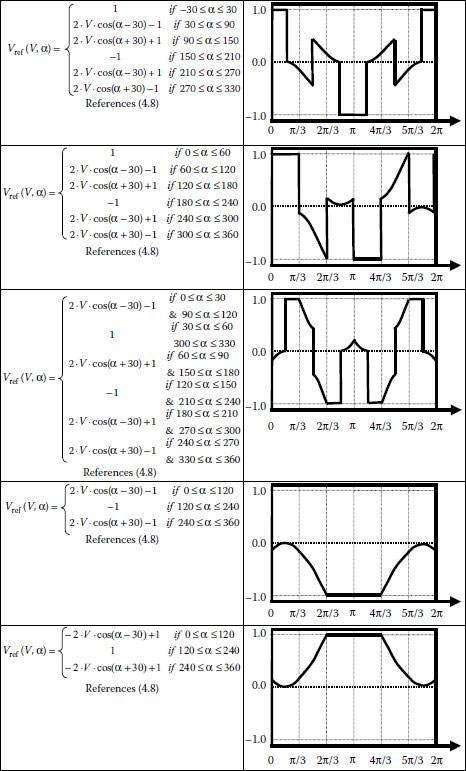
FIGURE 4.7 Possible modulator references for discontinuous PWM for a modulation index of 0.5.
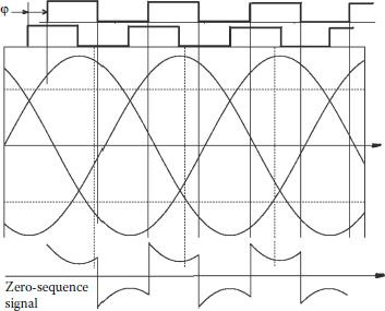
FIGURE 4.8 Generalized PWM generator.
First, note that the V/Hz characteristic used in control is not linear over the entire frequency range (Figure 4.9). At low frequencies, the magnitude of the reference voltage is small and the voltage drop on the resistive component of the stator is larger than the inductive voltage component. The reference magnitude, therefore, actually increases within the controller, accounting for the resistive voltage drop while the machine flux remains constant. Moreover, at high frequencies, the characteristic is limited in order to keep a constant voltage. This ensures control with a field weakening.
From the control and implementation of control perspectives, V/Hz control considers phase voltage generation in phase measures, with variations on a time scale referring more to the shape over the fundamental period. In contrast, modern vector control or field-orientation control assumes a high-frequency sample-and-hold of the drive system and a control independent of phase measures. Within a vector control system, the digital PWM generation does not use the desired shape of the phase voltage over a cycle, but the calculation of the instantaneous changes of these voltages (or currents) only. Volt per hertz control changes magnitude and phase while the vector-control method changes current references at a fixed sampling interval. Understanding this big difference emphasizes the advantage of using carrier based PWM in V/Hz control methods [4,5,6,12,16].
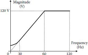
FIGURE 4.9 Real V/Hz characteristics.
It has been shown that for very large ratios between the carrier frequency and the frequency of the reference waveform, these two waveforms do not need to be synchronized to each other. However, for low-frequency ratios, waveform synchronization becomes mandatory and the frequency ratios may take particular values only (multiple of six).
4.3.1 OPERATION IN the LOW-FREQUENCIES RANGE (BELOW NOMINAL FREQUENCY)
In a motor drive application, the fundamental frequency varies over a wide range. On the other hand, the switching frequency must be contained due to power loss and thermal considerations. It is very difficult to satisfy both constraints using a single pattern of the PWM generator over the whole frequency range. The frequency ratio is generally selected to take different values on different fundamental frequency intervals, on the basis of the limits of the switching frequency or optimization of the HCF factor [4,5,6,12,16]. If we extend this method for power supplies that generate voltages with variable frequency and magnitude, we can optimize the number of pulses on the basis of filter requirements optimization. Let us analyze each method separately.
• Limit of the switching frequency: A possible solution is shown in Figure 4.10. For each frequency interval there is a linear relationship between the fundamental frequency of the reference and the carrier frequency (fsw). The slope of the characteristics equals the frequency ratio. To avoid system oscillations, transition between operation modes is ensured with a hysteresis. The solution shown in Figure 4.10 changes operation modes when frequency doubles, but similar controls can be defined for ratio values in a series like 24 → 36 → 48 → 60 → 72 or 18 → 36 → 72 → 144 → 288. Many industrial solutions go up to a frequency ratio of six for the last interval, ending up with a six-step not-modulated operation. The solution in which intervals are selected at double frequency is generally preferred because that reduces the number of transitions between operation modes and is simple to implement (see Chapter 8).
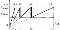
FIGURE 4.10 Use of different number of pulses on different intervals.
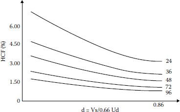
FIGURE 4.11 HCF for PWM with different number of pulses.
• Optimization of the HCF factor: HCF has been calculated for different frequency ratio methods and results are shown in Figure 4.11. If the application requires limiting this coefficient to below a given level, we can optimize the number of switching processes while still satisfying the harmonic requirement by selecting different frequency ratios for different frequency variation intervals (Figure 4.11) (see Chapter 3, Ref. 20). For instance, when a minimum value of 4% is considered, the maximum switching frequency is about 1.5 kHz. A limit to the frequency ratio must be assumed in the very low-speed range in order to simplify the digital implementation. Therefore, the HCF constraints will be relaxed for frequencies less than a few hertz. The proposed dependence of the sampling frequency fsw on the fundamental frequency f1 is presented in Figure 4.12 (see Chapter 3, Ref. 20).
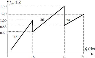
FIGURE 4.12 Sampling frequency versus output frequency.
• Filter requirements optimization for power supply applications: High-power power supplies operate at a constant frequency and with variable-voltage and are required to provide a low output impedance and less than 5% THD voltage content at load terminals. Their harmonic performance analyses have been considered in Section 3.5 and computer analysis results for DF in frequency ratios that equal 24, 36, 48, 72, and 96 have been shown in Figure 3.19. The proper frequency ratio can be selected from these results in order to keep DF below a certain value for any modulation index.
4.3.2 HIGH FREQUENCIES (>60 HZ)
In high frequencies that range from (60–120 Hz), a unique PWM pattern with a low number of pulses must be used independent of frequency and with a constant modulation index. This is generally optimized to reduce harmonics with lowest orders:
• Elimination of selective harmonics, such as the 5th or the 5th and 7th and so on, in the output phase voltage (Section 3.6).
• Global reduction of several low harmonics; for instance, minimization of the V25+V27.
4.4 IMPLEMENTATION OF HARMONIC REDUCTION WITH CARRIER PWM
Chapter 3 has provided solutions for specific harmonic elimination within three-phase inverters. Their implementation requires extensive off-line calculation and storage in memory look-up tables. This solution is not very advantageous for the control engineer. In contrast, this chapter has shown that carrier-based PWM is easily understood and implemented in modern microcontrollers without off-line calculation. Chapter 7 will further detail different implementation strategies within modern controllers. Some of these devices already have special peripherals for natural-sampled or regular-sampled carrier-based PWM. In the early 1990s, researchers considered these digital hardware platforms for implementation of harmonic elimination strategies [17].
Let us reconsider Figure 3.26 in Figure 4.13. Solutions for harmonic elimination for the line-to-line voltage (VLL) can be achieved below a modulation index of 0.866. The operation outside 0.866 can be artificially achieved by extending the angular solutions, as shown in Figure 4.13. As a coincidence, this also represents the maximum modulation index for a space vector modulation algorithm. Moreover, the dependency of the switching angles on the modulation index is linear up to approximately 0.69 and nonlinear between 0.69 and 0.866. Figure 4.13 also shows that odd switching angles have a negative slope whereas the even switching angles have positive slopes. All these characteristics start and end at points with a separation of
(4.3) |
where N is the number of switchings within a 60° interval (3 in our example).
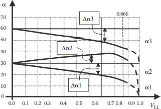
FIGURE 4.13 Switching angles for harmonic cancelation in VLL of a three-phase inverter.
Let us consider a regular-sampled PWM with this sampling interval (Ts). During each sampling period, control of the trailing and leading edges are supposed to be achieved separately according to the regular-sampled PWM approach. For each of these controls, sinusoidal reference waveforms are considered, as shown in Figure 4.14 and the switching angles are given by Equation 4.4 in absolute values from the beginning of the whole cycle.
k=oddαk=(k+1)Ts2−mTs2 sin [(k+1)Ts2+ϕ1]k=evenαk=(k)Ts2+mTs2 sin [kTs2+ϕ2] |
(4.4) |
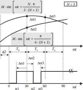
FIGURE 4.14 Equivalence between harmonic elimination and regular-sampled PWM.
The sinusoidal term is required for a microcontroller implementation of Equation 4.4, since the first term is already incrementally generated within the natural PWM algorithm. The magnitude of the reference sinusoidal waveform represents the modulation index (m) and it follows closely the desired amount of voltage on the load with an error less than 3.5%. The phase of these sinusoidal references can be determined with curve fitting at each sampling moment or with an approximate solution. The approximate solution uses:
(4.5) |
The resulting errors of this approximation are less than 0.25° at any operation point, leading to “cancelled” harmonics less than 2% [17].
For modulation indices between 0.69 and 0.866, the switching angle dependency on the modulation index is nonlinear, and the implementation on a regular-sampled PWM can be achieved by a nonlinear variation of the position of the sampling instants. The sampling period becomes smaller and smaller when the modulation index increases and all the sampling intervals are crowded toward 0°. Finally, all sampling moments coincide at 0° for the maximum modulation index, and square-wave operation is achieved.
4.5 LIMITS OF OPERATION: MINIMUM PULSE WIDTH
The circuit presented in Figure 3.2 is ideal and differences in operation will occur when switches are implemented with real semiconductor devices. Figure 3.2 also showed how current always commutes between a switch and a diode on the same leg. The PWM method can sometimes lead to short widths of the pulses to be applied on the load [18,19].
Transients in a real semiconductor device delay and narrow the shape of the voltage pulses achieved on the load. In extreme cases, the load does not see any clear voltage pulses while the power semiconductor devices are still switching. In other words, losses remain but the expected harmonic improvement on the load is not realized. Waveforms pertaining to such a case are shown in Figure 4.15.
In order to avoid the commutation at the power stage of short pulses, the most common methods employed are
• Pulse deletion: pulses are deleted from the PWM waveform if narrower than a certain amount and intervals with no switchings on the power converter occur. Waveforms resulting from this method are shown in Figures 4.16 and 4.17. One can see that the resulting load current has an increased content in fundamental and larger harmonics.
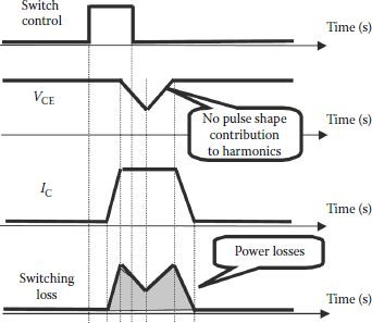
FIGURE 4.15 Switching waveforms for a short pulse.
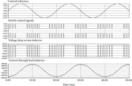
FIGURE 4.16 Effect of pulse dropping in the converter waveforms (converter from Figure 3.3).
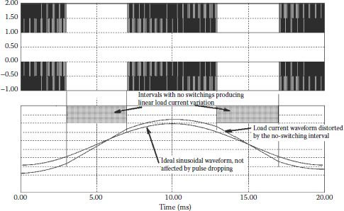
FIGURE 4.17 Effect of a very large pulse dropping interval (same converter at 10 kHz).
• Pulse limitation: pulses are limited to a predefined value if narrower than a certain amount and switches are transitioning at fixed pulse widths for some time. Waveforms resulting from this method are shown in Figures 4.18 and 4.19. The loss in fundamental is noticeable; the worsened content in harmonics is also noticeable.
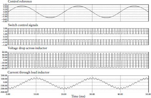
FIGURE 4.18 Effect of pulse limitation in the converter waveforms (converter from Figure 3.3).
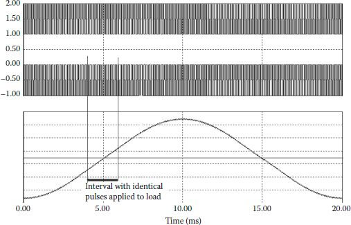
FIGURE 4.19 Effect of a very large pulse limitation interval (same converter at 10 kHz).
The pulse dropping region occurs at an especially high modulation index and the dependence of the fundamental component of the phase voltage on the modulation index is shown in Figure 4.20. Loss or gain of characteristics is more obvious at the high modulation index where generally high currents are also present.
The pulse-dropping region poses important problems for the control engineer. The system becomes nonlinear and controllability is lost during the intervals when pulses are limited or deleted. This ultimately leads to instabilities.
Many researchers have tried to find solutions to compensate for the pulse dropping effect or to avoid operation with narrow pulses. Compensation of the pulse dropping effect can extend linearity of the inverter transfer characteristics in high-modulation indices range.
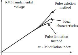
FIGURE 4.20 Fundamental voltage dependency on the modulation index.
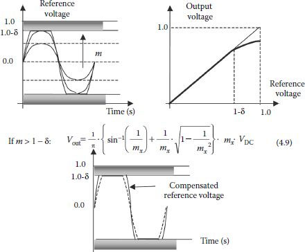
FIGURE 4.21 Compensation of the control (reference) voltage in order to achieve the desired linear dependence on the fundamental component.
Figure 4.21 shows how the real reference voltage signal is saturated at a level equal to 1 – δ, where δ is the accepted minimum pulse normalized. This normalization is made to the maximum available modulation index, which is 0.785 (or π/4).
To calculate its component on the fundamental frequency, we have to use the Fourier coefficient relationship:
A(1)=1ωT∫ωT0v(ωt)cos(ωt)dωt⇒vref=√A2(1)+B2(1)B(1)=1ωT∫ωT0v(ωt)sin(ωt)dωt |
(4.6) |
Let us denote mx as the magnitude of the voltage reference before saturation (larger than 1 for the considered normalization). The relationship between the modulation index and mx is given by
(4.7) |
The component on the fundamental frequency after saturation is calculated as
v(1)out=1π{sin−1(π4m)+[π4m]√1−[π4m]2}4mπVDC={[4mπ]sin−1(π4m)+√1−[π4m]2}12[2VDCπ]⇒v(1)out[2VDC/π]=12{[4mπ]sin−1(π4m)+√1−[π4m]2} |
(4.8) |
Several methods have proven useful:
• Increase of the voltage reference in inverse proportion with the falling transfer characteristic [11] with drawbacks on the dynamic range (Figure 4.21). Observing the limitation of the real reference voltage due to limitation of the pulse width provides a mathematical relationship between the modulation index and the real output voltage. A memory look-up table of the inverse relationship helps to compensate for the truncation of the transfer characteristics in order to get the desired fundamental component on the load.
• Adding a square-wave to the modulating voltage command [11] with drawbacks on the harmonic content of the phase currents, inverter, and machine losses (Figure 4.22). The magnitude of the square-wave (x) is calculated based on the magnitude of desired waveform (V) so that, after saturation at “1,” the same level of the component at the fundamental frequency can be kept.
• Other reshaping of the modulating commands with increased computational effort (Figure 4.23).
All these methods based on reshaping the reference voltage are not very suitable for motor drive applications due to the intensive computation required in real time. At each operating point, we would need to correct the reference waveform for linearity.
A completely different method consists of using staircase PWM or another PWM method that does not produce narrow pulses. The idea is to use a reference voltage with changes in the low frequency and sampled by the PWM generator at high frequency (Figure 4.24).
Using this method results in loss of resolution in defining the pulse width based on the sinusoidal reference waveform. This has effects on the harmonic content of the load voltage. Figure 4.25 shows what we gain by using this method while limiting pulses to a minimum pulse width and what we lose by using this staircase reference instead of a sinusoidal reference.
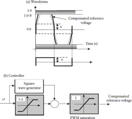
FIGURE 4.22 Reshaping the control (reference) voltage by adding square-wave functions: (a) waveforms; (b) controller.
4.5.1 AVOIDING PULSE DROPPING BY HARMONIC INJECTION [18]
The last solution reviewed in this chapter refers to a harmonic injection able to avoid small pulse widths. It has already been shown that the presence of the third harmonic in the switching function or pole voltage does not show up in the phase voltage. Since many years, this has been used to increase the linear transfer range of a three-phase inverter. It was originally required because only a low switching frequency was available from power semiconductor devices.
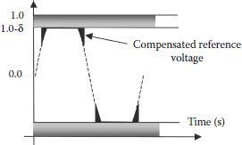
FIGURE 4.23 Reshaping the control (reference) voltage by adding square-wave functions.
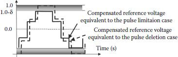
FIGURE 4.24 Principle of generating staircase PWM.
The same idea can be used along with high-frequency power semiconductor devices to avoid pulse dropping. This will modify the modulation waveform so that the pulse width is kept inside a desired bandwidth, as shown in Figure 4.26.
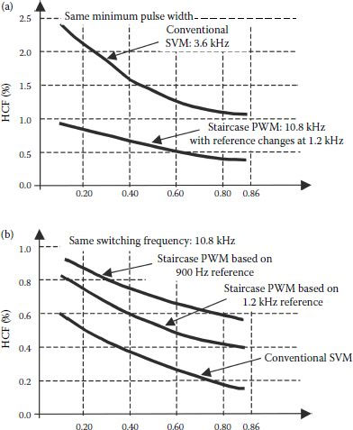
FIGURE 4.25 Different harmonic results for the load current. (Printed with permission of IEEE.)
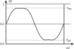
FIGURE 4.26 Limit the pulse width by third harmonic injection.
The pulse widths in the presence of the third harmonic are calculated with
(4.9) |
(4.10) |
(4.11) |
where θ is the angular coordinate. This is known from the methods using the third harmonic to increase the modulation range. These equations are easily implemented in a digital controller with center-aligned PWM generator. Examples of implementation will be shown in Chapter 9.
Considering that the only goal of this third harmonic injection consists of limiting the pulse width to avoid pulse deletion, the amount of the third harmonic can be calculated from the constraint of the minimum pulse.
The extreme points of any of PWMA, PWMB, or PWMC are given by
(4.12) |
The following solutions yield cos θ=√(9k−1)/12k and sin θ=√(3k+1)/12k[15] for θ < 90°, and PWMA hits its maximum at this point.
Generally, we have min PW < PWMA < max PW (Figure 4.26). For specific operating switching frequency (pulse period) and minimum pulse width, the maximum accepted pulse width will result automatically. Let us denote:
(4.13) |
Replacing the solutions sin θ and cos θ in the definition of PWMA (Equation 4.9) yields the following [15]:
xpu=m[sin θ+k[3 sin θ−4sin3 θ]]+12⇔(2xpu−1)m=[sin θ+k[3 sin θ−4sin3 θ]] |
(4.14) |
(2xpu−1)m=√3k+112k[1+k[3−43k+112k]]⇔(2xpu−1)m=√3k+112k23(3k+1) |
(4.15) |
[(2xpu−1)m]2=3k+112k49(3k+1)2⇔[(2xpu−1)m]2=3k+112k49(9k2+6k+1) |
(4.16) |
(4.17) |
(4.18) |
This polynomial equation has three solutions for each set of numerical values for the period of the PWM cycle, the desired minimum pulse width, and the modulation index. The smaller solution in absolute value is preferred in order not to increase the inverter ratings.
Let us take an example for a switching frequency of 12 kHz (83.3 μs), a modulation index of 1.0, and different constraints for the minimum pulse width. Table 4.1 [18] presents solutions for Equation 4.18 in each case. It can be verified that the sum of all solutions equals −1.
For modulation indices less than unity and identical constraints, the amount of the injected third harmonic is smaller. At low-modulation index, there is no need for harmonic injection. For instance, the dependence of k on the modulation index for a desired minimum pulse of 5 μs is presented in Figure 4.27.
This kind of dependency can be stored in a look-up table. The third harmonic needs to be injected in all three reference voltages and this can seem difficult in a vector-controlled converter where the (x,y) coordinates are available, but not the phase references. Moreover, the phase of the injected third harmonic can be difficult to estimate even from the phase references. However, the third harmonic can be calculated from the (x,y) coordinates with
TABLE 4.1
Solutions of Polynomial Equation
Min PW [μs] |
xpu |
Solution K3 |
Solution K1 |
Solution K2 |
0 |
1.0000 |
–1.4705 |
0.4089 |
0.0616 |
0.5 |
0.9939 |
–1.4580 |
0.3935 |
0.0646 |
1.0 |
0.9879 |
–1.4458 |
0.3780 |
0.0678 |
1.5 |
0.9819 |
–1.4335 |
0.3622 |
0.0713 |
2.0 |
0.9759 |
–1.4212 |
0.3459 |
0.0753 |
2.5 |
0.9699 |
–1.4089 |
0.3291 |
0.0799 |
3.0 |
0.9639 |
–1.3967 |
0.3115 |
0.0851 |
3.5 |
0.9579 |
–1.3844 |
0.2931 |
0.0913 |
4.0 |
0.9519 |
–1.3721 |
0.2733 |
0.0988 |
4.5 |
0.9459 |
–1.3598 |
0.2215 |
0.1083 |
5.0 |
0.9399 |
–1.3475 |
0.2257 |
0.1218 |
5.5 |
0.9339 |
–1.3352 |
0.1861 |
0.1491 |
Source: From Neacsu, D.O., Rajashekara, K., and Gunawan, F. Linear Control of PWM Inverter by Avoiding the Pulse Dropping, IEEE Workshop on Power Electronics in Transportation, Detroit, MI, USA, October 24–25, pp. 31–38. © (2002) With permission of IEEE.
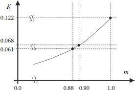
FIGURE 4.27 Optimal k-value for the considered example.
vt=mk sin (3θ)=mk sin θ(3−4sin2θ)=k√v2sx+v2syvsx√v2sx+v2sy[3−4v2sxv2sx+v2sy] |
(4.19) |
(4.20) |
This term should be added to each phase reference before using the center-aligned PWM generator hardware.
Using this approach within a motor drive helps to improve the phase current waveforms and removes the undesired distortion produced by the pulse width limitation algorithm. Comparative results are shown in Figure 4.28.
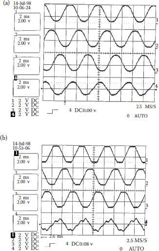
FIGURE 4.28 Vector control operation waveforms outlining the improved current waveform with the new algorithm. (a) The new algorithm for ids = 25 A, iqs = 80 A, m = 0.84; (b) pulse limitation method for sinusoidal PWM with ids = 25 A, iqs = 80 A, m = 0.84. (From Neacsu, D.O., Rajashekara, K., Gunawan, F. Linear Control of PWM Inverter by Avoiding the Pulse Dropping, IEEE Workshop on Power Electronics in Transportation, Detroit, MI, USA, October 24–25, pp. 31–38. © (2002) With permission of IEEE.)
The previous analysis of inverter operation considered ideal switchings within the inverter legs. However, Chapter 2 showed the ON/OFF transients of different semiconductor power devices. Any change of state requires a finite interval of time that should be considered in the design of the control circuitry.
For instance, if the command for turning on the low-side IGBT comes quickly after the command for turn-off of the high-side IGBT, a short circuit occurs through both devices. To avoid this, a delay is introduced in the control of the turning-on device after the other device is turned-off. This provides enough time for the turnoff process to finish. During this deadtime interval, both switches are assumed OFF [20,21,22,23,24,25,26,27] (Figure 4.29).
When IGBTs are used and not MOSFETs, this delay needs to be longer due to the tail of the collector current. This tail is produced by the charges stored in the p–n junction of the bipolar transistor. As the MOSFET channel stops conducting, electron current ceases, and the IGBT current drops rapidly to the level of the recombination current at the inception of the tail. Different modern IGBTs are optimized to reduce this tail current by speeding-up the recombination time with different lifetime-killing techniques. As they reduce the gain of the bipolar transistor, these techniques also increase the voltage drop and turn-on losses. Accordingly, there are some limits or constraints to speeding up the turn-off process. The tail current interval cannot also be improved through the gate control. Finally, transient characteristics are worse at higher temperature.
Introducing this delay in the switching sequence modifies the width of the pulses applied on the load and their average value. Accordingly, the waveform of the load current and its harmonic spectrum are also altered.
Keeping these in mind, a proper definition of the deadtime interval is mandatory. If the deadtime interval is too short, the possible short circuit can absorb a large current and the heat produced may damage the power semiconductor. If the deadtime is too long, the pulse shapes are more compromised and the current waveform more altered.
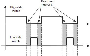
FIGURE 4.29 Deadtime.
A good practical method of estimating the length of the deadtime interval is to measure the DC current at the inverter input when no load is connected. Then, the only possible current would result from short circuits due to cross-conduction. This experiment can be carried out in several steps:
• Use a very large deadtime interval and start switching on one inverter leg. A small pulse of current will be seen on the DC-side, due to the dv/dt of the pole voltage through the Miller capacitance when switching occurs. This can account for about 5% of the power semiconductor rated current.
• Use a small deadtime interval. A larger current will be noticed on the DC side. It will depend on the length of the tail current remaining active when the other switch tries to turn on.
• Increase deadtime interval from this small value and observe the different shape and value of the pulse current through the DC side wires. The value of the deadtime interval is best selected when this current approaches the initial value.
These tests are more useful when done at high temperature. Usually, deadtime is generated with a delayed turn-on event, as shown in Figure 4.30.
After the deadtime interval value has been properly selected, it becomes important to understand how much performance is lost due to the delay in the switching intervals. As both switches on the same leg are supposed to be turned-off during the deadtime interval, the load current temporarily turns-on the antiparallel diode that maintains the current circulation. If the load current is positive (it circulates from power converter to the load), the low-side diode will turn on after the high-side switch is turned off (Figure 4.31). This determines the loss in the load voltage as compared to the ideal switching pattern. The pole voltage error during the pulse depends on the width of the deadtime and DC bus voltage.
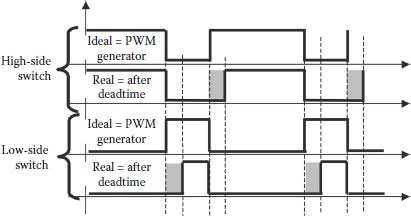
FIGURE 4.30 Practical generation of deadtime by delaying the turn-on of each power device.
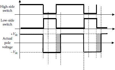
FIGURE 4.31 Effect of positive load current during deadtime.
In contrast, if the load current is negative (it circulates from load to the power converter), the load voltage gains something on its positive side (Figure 4.32). The amount of voltage error again depends on the width of the deadtime and the DC bus voltage.
On both positive and negative load currents, the amount of voltage error is constant throughout the modulation cycle and does not depend on the desired width of the pulses. The error voltage is shown in Figure 4.33. It is important to note that the amount of error voltage does not depend on the magnitude of the reference voltage (modulation index). The voltage error is larger at low modulation indices, such as in the case of V/Hz drives operated at low speeds.
This analysis assumes identical transients of the power switches at all moments during the cycle. This approximation is not exact as it has been proven that the transient slopes and delays of the power devices depend on the level of the current to be switched and the voltage on the DC bus. Voltage error is best analyzed by direct measurement of the load voltage.
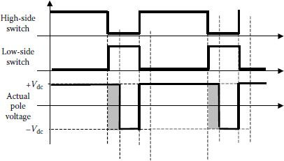
FIGURE 4.32 Effect of negative load current during deadtime.
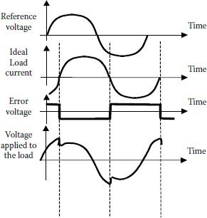
FIGURE 4.33 Voltage error is based on load current sign and load power factor (phase shift).
Applying voltage waveforms distorted by deadtime to a three-phase load would produce distortion of the current at each 60°. Each phase current will tend to be distorted twice during the modulation cycle and the effect of this distortion on the load current will obviously pass through the other two phases when the power converter from Figure 3.11a is considered.
This analysis outlines the following major drawbacks produced by deadtime:
• There is a clear difference between the voltage reference and the actual voltage applied on the load.
• Inverter output current has a 6th harmonic component that can be seen on the phase, the (d, q) components of the current, or on the torque ripple.
Several methods have been proposed for deadtime compensation:
• Voltage compensator based on hardware circuitry: A circuit is built to measure the actual load voltage and to compare it with the desired reference based on the current sign. The difference is always applied to the next pulse. There is an intrinsic phase shift in the applied voltage and this is the main problem of this method.
• Voltage feedback through a proportional-integral (PI) compensator: A real PI controller is built up from the error between the measured and reference voltages. The result is used as a compensation voltage added to the actual reference signal. This method is not suitable for fast switching converters, but for converters based on slow devices such as gate turn-off thyristors (Figure 4.34).
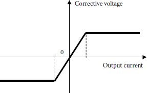
FIGURE 4.34 Modified corrective voltage for deadtime compensation.
• Pulse-based deadtime compensator: This method adjusts each pulse width on the basis of the previous pulse voltage by using symmetry of the output waveform. It is not very sensitive to fast load current changes.
• Current feedback compensator: This method adds or subtracts an amount from the desired pulse width based on the sign of the current. It works on open-loop and the goal is to approximate the deadtime effect for quasi-identical transient events. An improvement of this method is to modify the corrective amount added to the reference voltage depending on the current level. The same amount of pulse width is added for larger currents, but small currents imply a reduction of the corrective voltage.
The current feedback compensator method is the simplest to be implemented in a PWM converter working with a switching frequency of 8–20 kHz and controlled from a digital signal processor or microcontroller device. Compensation is achieved at each sampling interval with sign detection for each phase current and algebraic addition of a constant in the voltage reference waveform. This three-phase power converter is used for a motor drive application and results can be noticed at any motor speeds.
Another distortion of the output current in a real three-phase power converter refers to the zero current clamping (Figure 4.35). It is already known that a power semiconductor device cannot conduct very small load currents. When current is near zero, the power device remains on the OFF state and the load current is “clamped” at zero. This state lasts for a time interval that depends on the power device used within the three-phase converter, the amount of inductive components on the circuit, the operating frequency, and the magnitude of the current. For a given power semiconductor device and circuit, the slope of the current at zero crossing defines the length of the zero current clamping interval. Assuming a quasi-sinusoidal waveform for the current, this slope (di/dt) depends on the current magnitude and the frequency (di/dt = 2 * π * f * I) (Figure 4.36). This figure does not include the effect of dead-time. The presence of a large deadtime increases the width of the zero-current clamping interval.
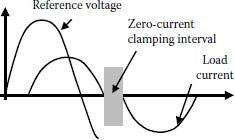
FIGURE 4.35 Zero current clamping.
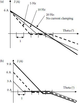
FIGURE 4.36 Zero-current clamping dependence on current frequency and magnitude.
Carrier-based modulation provides a linear characteristic up to the modulation index of 0.785. Deadtime and minimum pulse width constraints reduce further the linear region, as has been shown earlier. The interval between the maximum obtainable modulation index and the six-step operation is called overmodulation [28,29,30,31,32]. Inverter operation during this interval is characterized by nonlinearity and instabilities of the feedback controllers. This and other problems led engineers to design special PWM algorithms able to provide full inverter voltage utilization and linearity up to the six-step operation.
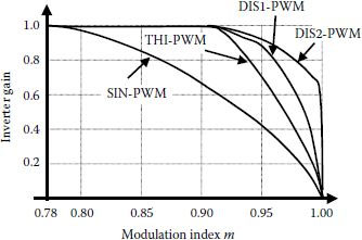
FIGURE 4.37 Inverter voltage gain.
Analysis of the saturation of any of the voltage references presented earlier is made with the same mathematics. An inverter voltage gain is defined and its dependence on the desired modulation index is shown in Figure 4.37. Another form for the same results is presented in Figure 4.38 and it can be considered as a zoom on the final part of the transfer characteristic between the control (desired) reference and the real modulation index calculated with respect to a six-step operation.
These PWM algorithms need very large reference signals in order to operate in the overmodulation range. For instance, conventional sinusoidal PWM requires a magnitude more than four times that of the sinusoidal reference to operate at six-step. The quickest variation is achieved for the discontinuous modulation: six-step operation is achieved for a modulator magnitude of 1.81.
4.6.3.1 Voltage Gain Linearization
The simplest solution to achieving six-step operation is to increase the magnitude of the reference voltage [33]. Another solution can be defined analogously with the minimum pulse compensation methods by adding square-waves to the reference. Both solutions require extensive off-line calculation and storage in a look-up table.
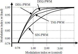
FIGURE 4.38 Inverter voltage gain.
Compared with the uniform-sampled PWM implementation, the sine-triangle intersection method provides simpler overmodulation algorithms. Digital implementation of the uniform-sampled PWM method requires software preparation of the overmodulation operation based on calculation of the function to be added to the reference.
Even if overmodulation can be carried out with one of these methods, the performance is strongly affected during overmodulation operation and it is recommended only for dynamic or transient operation. Among the methods studied, discontinuous PWM provides better performance and less influence on the deadtime and minimum pulse. Finally, vectorial analysis of PWM algorithms and definition of space vector PWM allows easier definition of the overmodulation algorithm.
Chapter 3 has presented a simple method for generation of PWM signals based on the intersection between a sinusoidal and a triangular waveform. Problems associated with implementation and use of this principle in a three-phase inverter are detailed in this chapter. Inverter operation is unfortunately affected by minimum pulse width, deadtime selection, and maximum available voltage. Solutions for compensation for each of these effects have been shown and improvements also presented.
P4.1 |
The conventional PWM method produces switchings of the inverter’s IGBTs at intersection of a sinusoidal waveform and a high-frequency triangular signal. The intersection moments are not easy to be expressed mathematically. How are they influencing the harmonic content of the output phase voltage? |
P4.2 |
Use a computer program with graphical features and draw the dependence of Equation 4.8 or 4.9 for large modulation indices. Consider δ = 0.10. |
P4.3 |
For the same numerical example, calculate the magnitude of the compensation square-wave of Figure 4.22. |
P4.4 |
How should the Staircase PWM be synchronized with the fundamental in order to obtain the most favorable value of the minimum pulse width? |
P4.5 |
Remake all calculus shown by Equations 4.15, 4.16, 4.17, 4.18, 4.19 for a PWM with 20 kHz and a minimum pulse of 3 μs. How much is the resulting third harmonics at a modulation index of 1.00? Use a computer program and draw the appropriate dependence on modulation index. |
P4.6 |
Equation 4.8 has been determined for sinusoidal modulation when the magnitude of the sinusoidal reference is exceeding 1.00 (or a modulation index of 0.785). Determine a similar relationship for the component on the fundamental frequency after saturation when a third harmonic injection is considered with a magnitude of 0.25 of fundamental. |
P4.7 |
Consider a high power three-phase IGBT inverter operated at 10 kHz with a fixed deadtime of 4 μs and a fixed modulation index of 0.5 (modulation index is defined in respect with the six-step operation). Neglect the actual transients of voltage and currents at IGBT switchings and calculate the RMS value of the error in the phase voltages. Represent this voltage as percentage of the actual load phase voltage. |
P4.8 |
Consider a sinusoidal function with a magnitude of 2.00 but limited on both positive and negative segments at 1.00. Calculate the RMS value of the fundamental of the waveform thus obtained. If the sinusoidal waveform magnitude equal to 1.00 corresponds to a modulation index of 0.78, what value of the modulation index corresponds to the new waveform? |
1. Buja, G.S. and Fiorini, P. 1980. A microprocessor based quasi-continuous output controller for PWM inverters. IEEE International Conference on Industrial Electronics, Philadelphia, PA, pp. 107–111, March.
2. Buja, G.S. and Indri, G.B. 1975. Improvement of pulse width modulation techniques. Archiv fur Elektrotechnik 57, 281–289.
3. Houndsworth, J.A. and Grant, D.A. 1984. The use of harmonic distortion to increase voltage of three-phase PWM inverter. Trans. IA 20(5), 1224–1228.
4. Scorner, J. 1975. Bezugsspanung zur umrichterssteuerung. ETZ-b 27, 151–152.
5. Depenbrock, M. 1977. Pulse width control of a three-phase inverter with nonsinusoidal phase voltages. Conference record, IEEE International Semiconductor Power Conversion Conference, pp. 399–403.
6. Rajashekara, K.S. and Vithayathil, J. 1982. Microprocessor based sinusoidal PWM inverter by DMA transfer. IEEE Trans. IE 29, 46–58.
7. Lucanu, M. and Neacsu, D. 1995. Optimal voltage/frequency control for space vector PWM three-phase inverters. ETEP 5(2), 115–120.
8. Legowski, S. and Trzynadlowski, A. 1993. Minimum loss vector PWM strategy for three-phase inverters. IEEE IECON, pp. 785–792.
9. Chung, D.W. and Sul, S.K. 1997. Minimum loss PWM strategy for three-phase PWM rectifier. IEEE PESC, pp. 1020–1026.
10. Trzynadlowski, A. and Legowski, S. 1993. Minimum loss vector PWM strategy for three-phase inverters. Applied Power Electronics Conference and Exposition, APEC’93, San Diego, CA, USA, pp. 785–792, 7–11 March.
11. Hava, A., Kerkman, R., and Lipo, T.A. 1998. A high-performance generalized discontinuous PWM algorithm. IEEE Trans. IA 34(5), 1059–1071.
12. Narayanan, G. and Ranganathan, T. 2002. Two novel synchronized bus-clamping PWM strategies based on space vector approach for high power devices. IEEE Trans. PE 17, 84–93.
13. Lai, R.S. and Ngo, K.D.T. 1995. A PWM method for reducing of switching loss in a full-bridge inverter. IEEE Trans. PE 10, 326–332.
14. Trzynadlowski, A., Kirlin, R., and Legowski, S. 1997. Space vector PWM technique with minimum switching losses and a variable pulse rate. IEEE Trans. IE 44, 173–181.
15. Faldella, E. and Rossi, C. 1994. High efficiency PWM technique for digital control of DC/AC converters. IEEE APEC, pp. 115–121.
16. Bose, B.K. and Sunderland, A. 1983. A high performance PWM for an inverter fed drive system using a microcomputer. IEEE Trans. IA 19, 235–243.
17. Bowes, S. and Clark, P. 1995. Regular-sampled harmonic elimination PWM control of inverter drives. IEEE Trans. PE 10(5), 521–531.
18. Neacsu, D., Rajashekara, K., and Gunawan, F. 2002. Linear control of a PWM inverter in the pulse dropping region. IEEE WPET, pp. 37–47.
19. Kerkman, R., Seibel, B., and Legate, D. 1992. PWM control in the pulse dropping region. U.S. Patent 5,121,043.
20. Kimball, J. and Krein, P. 1997. Real-time optimization of deadtime for motor control inverters. IEEE PESC, vol. 1, pp. 597–600.
21. Murai, Y., Riyanto, A., Nakamura, H., and Matsui, K. 1992. PWM strategy for high-frequency carrier inverters eliminating current-clamps during switching dead-time. Industry Applications Society Annual Meeting, Houston, TX, vol. 1, pp. 317–322, 4–9 October.
22. Choi, J.W. and Yong, S.I. 1994. Inverter output voltage synthesis using novel dead-time compensation. IEEE PESC, pp. 100–106.
23. Choi, J.W. and Sul, S.K. 1994. New dead time compensation eliminating zero current clamping in voltage-fed PWM inverter. IEEE IECON, pp. 977–984.
24. Ben-Brahim, L. 1998. Analysis and compensation of dead-time effects in three-phase PWM inverters. IEEE Industrial Electronics Society, Aachen, Germany, vol. 2, no. 31, pp. 792–797, 31 August–4 September.
25. Legate, D. and Kerkman, R. 1997. Pulse-based dead-time compensator for PWM voltage inverters. IEEE Trans. IE 44(2), 191–197.
26. Munoz, A. and Lipo, T.A. 1999. On-line dead-time compensation technique for open-loop PWM-VSI drives. IEEE Trans. PE 14(4), 683–689.
27. Kameyama, T. 1999. Inverter control device. U.S. Patent 5,872,710.
28. Hava, A., Kerkman, R., and Lipo, T.A. 1998. Carrier-based PWM-VSI overmodulation strategies: Analysis, comparison and design. IEEE Trans. PE 13(4), 674–689.
29. Kerkman, R., Leggate, D., Seibel, B., and Rowan, T. 1993. An overmodulation strategy for PWM voltage inverters. IEEE IECON, pp. 1215–1221.
30. Floricau, D., Fodor, D., Ionescu, F., and Hapiot, J. 1996. Extension of the two-level SVM control strategy for the overmodulation area including the six-step mode, Int’l Conference OPTIM, Brasov, Romania, pp. 1471–1478.
31. Khambadkone, A. and Holtz, J. 2002. Compensated synchronous PI current controller in overmodulation range and six-step operation of space vector modulation based vector controlled drives. IEEE Trans. IE 49(1), 574–581.
32. Kaura, V. and Blasko, V. 1996. A method to improve linearity of a sinusoidal PWM in the overmodulation region. IEEE PEDES, pp. 325–331.
33. Kerkman, R., Leggate, D., Seibel, B., and Rowan, T. 1993. Inverter gain compensation for open-loop and current regulated PWM controllers. IMACS-TCI, pp. 7–12.