
6.1 SELECTION OF POWER DEVICES IN A THREE-PHASE INVERTER
Previous chapters have explained the operation of a three-phase converter and the need for pulse width modulation (PWM). This chapter investigates the three phase power converter as a system, outlining packaging and protection problems.
Power semiconductor devices for a three-phase power converter should be selected after determining the power converter ratings from the application requirements and taking into account the cooling and stress requirements for a given power level.
When the power converter is used within a motor drive, its rating depends on the motor characteristics as it follows.
The application should provide information about the maximum torque required.
The power converter should take into account an increase of about 60% torque availability as an overload. Sometimes, this overload is considered within the rated torque with a derate of the nominal torque.
6.1.1.2 Maximum Current Available
The maximum phase current can be derived from the nominal power on the motor data.
6.1.1.3 Maximum Apparent Power
The power converter must be able to process the whole apparent power, including the active power that produces torque and circulates reactive power.
6.1.1.4 Maximum Active (Load) Power
The maximum power processed by the power converter can be calculated if the efficiency and cost of the motor at a fixed operation mode are known. This criterion is not very effective as both these vary highly with the mode of operation.
After the motor data has been investigated for power converter ratings of maximum phase voltage and currents, selection of power semiconductor switches should be made including additional margins required for overvoltage and overcurrent.
The power is transferred from the grid mainly on fundamental frequency and the power semiconductor switches can be rated for their active power and a tolerable power factor. The fixed grid voltage automatically sets a fixed maximum voltage on the power semiconductor switches. Both current and voltage can be considered, respectively, with overvoltage and overcurrent. Modern snubberless converters do not require an overvoltage rating consistently larger than the operation voltage across the power semiconductor device.
Once we have a rough idea of the maximum levels of currents and voltage on power semiconductor switches, we have to check the cooling system. Appropriate switching power or energy losses for the required current level can be calculated based on the device model or estimated from device datasheets. For instance, Powerex insulated gate bipolar transistors (IGBTs) provide all switching energy losses estimated for different operation conditions. The switching losses are added to the conduction losses of each power semiconductor device to determine the cooling requirements. The datasheet also provides information about the junction-to-case thermal resistance for each semiconductor package.
The application should also provide information about the cooling system (air or coolant) and the temperature and pressure of the coolant agent. Simple equations determine the change in temperature under these cooling conditions, when the power loss is known. If the system has to work at a high temperature, an iterative process in a larger power device should be considered. There are some cases when the thermal requirement becomes more important than the maximum current. For instance, a 27 kW/300 V/90 A IGBT-based DC–DC power converter used in automotive applications may have the inlet coolant at 90°C. Selecting 100 A devices produces a junction temperature higher than recorded in the device datasheet.
Iterative design leads to selection of 300 A devices in order to overcome this thermal constraint. Higher current devices have lower thermal resistance because they have a different technology and can cope better in high temperature conditions. In many cases, this solution is cheaper than considering a more sophisticated cooling system with a lower thermal resistance.
Power semiconductor devices should be protected against extreme operating conditions and faults. Several protection requirements have become standard for power converters at any power level.
A very large value of the current can pass through a power semiconductor switch for diverse operational reasons. Let us try to understand the main sources of overcurrent and the means of electronic protection before the fuses burn.
Insulation breakdown or wrong connections can produce a short-circuit between two output wires (phases) (Figure 6.1). A simple shunt resistor followed by a linear optocoupler or a Hall-effect sensor on the DC bus can detect the unexpected peak of the current. Another protection method consists of using the same phase current sensors that are used for current control. Each phase current is compared against two extreme thresholds for positive and negative levels.
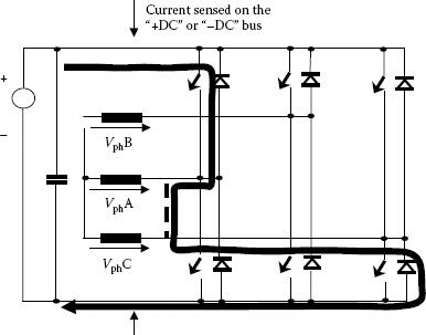
FIGURE 6.1 Short-circuit between two phases.
Ground fault is another possible source of overcurrent and it may be caused by a motor insulation breakdown to the ground (Figure 6.2). This source of overcurrent can also be detected with one of the previous methods: sensing either the DC current or each phase current. It is important to note that many industrial power converters controlled with vector-control methods do not measure all three-phase currents, but only two. They count on the symmetries of the three-phase system and calculate the third phase current as a difference between the sum of the other two currents and zero. Such a system cannot detect the ground fault if it occurs in the third phase.
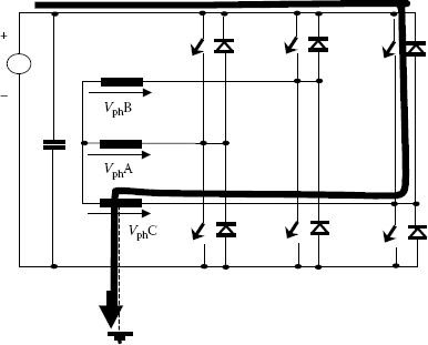
FIGURE 6.2 Ground fault.
Accordingly, a ground fault-protected system must sense all the three-phase currents.
Another source of undesired large currents arises from the shoot-through or cross-conduction fault. In certain conditions, the turn-on of an IGBT can produce a large positive (dv/dt) across the other IGBT on the same leg. Due to the Miller effect, this voltage variation can be accidentally transformed into gate current and turn-on the second IGBT. This would produce simultaneous conduction of both IGBT devices and short-circuit of the DC bus (Figure 6.3).
A general approach for protection consists of sensing voltage across each IGBT to prevent voltage build-up when the IGBT is in a controlled ON state. There are many circuit possibilities to implement this method: all of them sense the collector–emitter voltage and compare it with a fixed reference. Exceeding the reference shuts the gates off.
A simple circuit designated for this protection is shown in Figure 6.4 and it is called Desat protection. This name comes from the bipolar transistor’s saturation, and basically this circuit verifies if the controlled power semiconductor is really in the normal ON state (or “saturated” for a bipolar transistor). The voltage drop on the switch is sensed and compared with a reference defined by a Zener diode.
If the transistor is unsaturated, the voltage drop is higher than the specified value, and the hysteresis comparator inhibits the control signal, turning-off the power semiconductor switch.
It is important to note that any of these three sources of overcurrent (line-to-line, ground, or shoot-through) can trigger the system protection in order to shut-off all six gates of a three-phase inverter. A quick shutdown generally produces a large voltage spike due to inductive components’ tendency to keep the current circulating. This can be prevented by a soft shutdown of the IGBT under overcurrent, paying the price, though, of increased complexity of the control circuit.
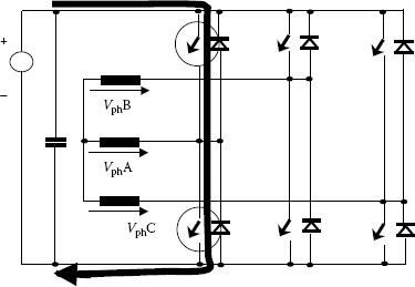
FIGURE 6.3 Shoot through.
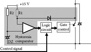
FIGURE 6.4 Desat protection.
The soft shutdown method shuts the gates off with a large gate resistor that is able to slow-down the turn-off waveforms. Synchronization of shutdown for all six gates implies additional complexity of the control circuitry. For this reason, the soft shutdown is used at low power levels where integrated circuits (IC) technology can easily accommodate the extra circuitry. International Rectifier Corporation has a nice series of high-voltage (600 and 1200 V) gate drivers (IR21xx and IR22xx) able to perform soft shutdown in the horsepower range.
Processing power in high-voltage circuits implies also protection against overcurrent and, especially, short-circuits. Fuses represent the most known method of overcurrent protection. A fuse is a device able to break a high current through its own damage under the heat generated by that current. Figure 6.5 presents the structure of a fuse.
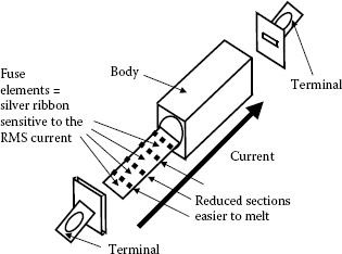
FIGURE 6.5 Basic structure of a fuse.
Current through the fuse produces heat, especially in the reduced sections. At high currents, these regions melt and the fuse is damaged. The rated current of the fuse is the maximum current carried continuously by the fuse without damage. This continuous current rating is defined with test procedures given in IEC269 or UL248 standards for ambient temperature, open air, and AC voltage at 50 or 60 Hz (grid). Another standard UL198L (DC Fuses for Industrial Use) provides the DC rating of the fuses in industrial applications.
An important parameter of a fuse is I2t (squared RMS current multiplied by the clearing time) and it defines the fuse melting under a high fault current (Figure 6.6) [1]. The fuse can also melt when a lower current passes through the fuse for a longer time. This defines a dependency of the melting time that is inversely proportional to the applied current (Figure 6.7).
Selection of fuses for protection of a power converter depends on the voltage, total RMS current, the semiconductor device’s rupturing I2t value, device current di/dt, circuit inductance, ambient temperature, style of connection, and so on [1,2,3]. Diodes and other rectifier semiconductors are provided with datasheet information on a half-cycle surge rating characterized by the magnitude of a single sinusoidal half-cycle pulse at 50 or 60 Hz that the device can withstand. This value along with the half-cycle length (8.33 or 10 ms) is considered to calculate the semiconductor I2t value.
Fuse selection is dependent on the total current containing both fundamental and harmonics and this is especially important in IGBT fusing. The high-switching frequency influences through the skin and proximity effects that are caused by nonuniform distribution of current density in the fuse elements. These effects are not very clearly known or defined, but they may justify premature opening of the fuse under the switching frequency components. A complete analysis of the power dissipation in a fuse under harmonics is presented in [4].
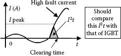
FIGURE 6.6 Fuse action on high fault current.
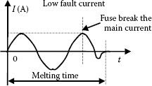
FIGURE 6.7 Melting of the fuse due to long-term current.
When a short-circuit occurs in an IGBT-based circuit, the collector–emitter voltage tends to increase immediately to a high value, which rapidly increases the internal power dissipation and failure of the device. Electronic protection circuits have been presented in the previous section. A fuse is used as protection when the electronic protection fails or is not used. The presence of the unprotected short-circuit in an IGBT can produce IGBT rupture, melting of the emitter connections or of the other circuit wires. If the IGBT rupture I2t data is missing, a good practice is to calculate the I2t for the copper bonding wire:
(6.1) |
where S is the wire section in mm2.
This will ensure lower values than those experimentally defined for the IGBT case.
There are several possible distributions of fuses within a power converter. A complete solution includes protection on the DC bus, on phase currents, and on all IGBTs. This is not totally justified and a simpler or cheaper solution is generally satisfactory. The best compromise for the position of fuses within a three-phase inverter is shown in Figure 6.8.
When the fuse needs to break an inductive current within a DC circuit, the value of the circuit inductance determines the clearing time. The larger the inductance, the harder it is for the fuse to break the current. If a fuse is capable of suppressing a given amount of energy, then the DC voltage rating of a fuse is only valid for a specific time constant influenced by the amount of inductive component. For instance, a typical time constant for a capacitor bank, battery supply, and distribution circuits or UPS inverters is less than 10 ms, the DC motor armature has a typical time constant of 20–40 ms, and a traction system has a time constant of less than 100 ms.
Table 6.1 shows the entire UL (Underwriters Laboratory) classification of low-voltage fuses (Hundred of Volts). The “branch-circuit” rated class fuse is the most robust of the DC fuses. While the catalog number may vary from a manufacturer to another, these fuses fall into several classes, each having different performance characteristics and sizes. Such classes are: RK-1 and RK-5 (0.1–600 amps), T (1–1200 amps), and CC (0.1–30 amps). Among them, the most popular, the RK-1 and RK-5 fuses fit in the fused, safety-switch disconnects available from all electrical supply houses and many home centers. These RK fuses are grouped in sizes by voltage with the shorter sizes having a 125-volt rating and longer sizes having a 250 or 600-volt DC rating. They are also grouped by current range (0.1–30, 35–60, 70–100, 110–200, 225–400, and 450–600 amps).
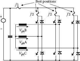
FIGURE 6.8 Best (reduced) placement of fuses.
In North America, fuses for medium voltage applications (kV range) fall within one of the following categories:
• “E” fuses are generally used for transformers and general-purpose applications.
• “E”-rated fuses for under 100 A must melt in 300 s at an RMS current within the range of 200–240% of the fuse’s continuous current rating.
• “E”-rated fuses above 100 A must melt in 600 s at an RMS current within the range of 240–264% of the fuse’s continuous current rating.
• “R” fuses are used for motors with high starting currents and generally are back-up fuses that provide short-circuit protection for motor circuits.
• R-rated fuses will melt in a range of 15–35 s at a current equal to 100 times the “R” rating.
The mounting of fuses on the busbar or printed-circuit-board should ensure a minimal electrical resistance of the contact, and under the assumption that the mounting support will sink heat from the fuse and not contribute to the fuse heating.
Power semiconductor devices are usually rated at a junction temperature between −40° and 150°C. Automotive, aerospace, or military applications require semiconductors rated below −40° or above 150°. For instance, power electronics for hybrid vehicles use the same cooling path as the engine providing a coolant at 90°. MOSFET devices are available today at 175° or 200° junction temperature. The advent of silicon carbide-based power devices will make possible operation above 250°.
A direct junction temperature measurement is very difficult. There are IGBT devices available in the market with junction temperature measurement based on a sensing diode on the same package, but they are expensive and, therefore, not widely used.
The most common approach to overtemperature protection consists of a temperature sensor on the cold plate or heatsink supporting the IGBT. If this thermocoupler is mounted as close as possible to the IGBT, it provides a good reading of the device package’s temperature. The measurement circuit is followed by analog processing. Unfortunately, the thermocoupler sensor is not linear and a linearization curve is needed if the temperature really needs measuring. This can usually be achieved by software using a piece-wise linearization method. Overtemperature protection does not really need this linearization or precise measurement, but requires only a comparison with a reference threshold in order to trigger the shutdown process.
Additional temperature monitoring is needed for the cooling system: this is either air-based or liquid-cooled. Some systems cooled with liquid also check the pressure.
DC bus voltage and phase voltages are also monitored. If overvoltage on the DC bus is detected, the IGBTs within the three-phase inverter need to be shutdown. Power electronics systems may require monitoring of the phase voltages and shutdown in case of overvoltage. Circuits for voltage monitoring are based on resistive or transformer `sensing of voltage followed by comparison with required thresholds. In high voltage, insulation with transformers from the power wires is required.
Except for these accidental overvoltage faults demanding fast action from the gate controller, overvoltage with slower transients is suppressed with devices called surge arrestors. This type of overvoltage can occur, for instance, at connection of a power electronics circuit to the power lines.
There are two classes of surge arresters: crowbar protection and clamping protection.
A crowbar device starts to conduct due to a quick change of its impedance when subjected to a large voltage. During this conduction interval, the voltage drop across the crowbar is limited to less than 15 V, allowing a large current to pass through it. It may be used in association with a dissipation resistor, a current-limiting device, or in series with a fuse that may blow due to the large current produced when the crowbar conducts. The energy is not dissipated on the crowbar device itself. The crowbar technique is also used in low-voltage DC/DC voltage regulators.
The most commonly used crowbar devices are air-gap protector, carbon-block protector, gas-discharge tube, and silicon-controlled rectifier (thyristor).
The second group of surge arrestors is composed of clamping devices. A clamping device varies its internal resistance to limit the voltage transient by absorbing some of the transient energy. This is a serious limitation during application at large currents. Possible devices in this group are Zener diodes and metal oxide varistors (MOVs). MOV devices are mostly used in power converter applications. They have a voltage variable resistance and can support large currents during protection. However, they tend to degrade over time if high peak currents are repeated.
Varistor protective devices have peak current ratings from 20 A–70,000 A, peak energy ratings from 0.01 J–10,000 J, and mounting options to serve a wide range of applications. There are two major classes of products:
• Multilayer Varistor (MLV) family consists of compact surface mount devices with enhanced performance and filtering characteristics for circuit board level applications. They protect against electrostatic discharge, EFT and surge, offer low capacitance for high data rates and high capacitance for EMI filtering, and are widely used in computers, handheld devices, and automotive electronics.
• Metal Oxide Varistor (MOV) family is the most suitable to the circuits presented in this thesis. They suppress higher energy voltage transients such as those generated by electrical load switching, they are offered in mounting options including bare disk, terminal connection, or radial and axial leaded packages.
MOV devices have a low power dissipation capability and they will be destroyed by repetitive transients. The MOV’s lifetime should be carefully considered in accordance with the particular operation.
The transition of current between a power semiconductor switch and a diode has been explained in Chapter 2. Once current has been transferred from the turning off device to the turning-on device, the voltage starts to swing. This hard-switching induces a time interval during which both current and voltage are large in the turning-on device. As shown in Figures 2.2 and 2.7, this stress is more important for inductive loads due to the overvoltage produced by the current variation (di/dt).
Trajectories in the (IC, VCE) corresponding to the real operation are shown in Figure 6.9. They depend upon stray inductances, parasitic capacitances, and IGBT switching performances as di/dt, dv/dt. For instance, the IGBT package itself has a stray inductance of few tens of nanoHenries (nH) (for devices of the order of hundreds of amperes). The largest parasitic inductance is introduced by the DC bus connection of the inverter. It is very important to minimize the circuit parasitic inductances with a proper layout design [5,6].
Factors as di/dt, dv/dt can be partly adjusted through the gate circuit and the operation area can be minimized inside the datasheet safe operating area. The over-voltage produced by the recovering diode can also be limited by increasing the gate resistor.
It may be necessary to limit the slope of the current at turn-on of a power semiconductor device by inserting a series inductance. This is not usually the case in modern devices, but is required for some gate turn-off thyristors (GTO) or bipolar transistor-based inverters. Since the switching current adds up to the recovery current of the diode, sometimes an alternative solution consists of using a saturable inductor with a ferrite core in series with the diode. This inductor is supposed to take over all the voltage during recovery and it may reduce the recovery current.
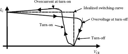
FIGURE 6.9 Trajectories during operation within a real circuit.
At turn-off, it may be necessary to limit the slope of the voltage. A better limitation along with power loss reduction can be achieved with snubber circuits [7] (Figure 6.10). When the snubber circuit is missing, the voltage will resonate due to the semiconductor parasitic capacitance and connections’ inductance. The snubber circuit has to dump these oscillations.
For low-power applications, the parasitic inductance of the IGBT package and mounting on the bus bar are smaller than the inductance of the DC link. This is the case of discrete IGBTs or IGBT-based power modules used in applications above tens of amperes. Using power modules is definitely better as all connections are inside the package with extremely low parasitic inductances. The common solution consists of a simple decoupling capacitor across the entire inverter leg, providing a noninductive path for current transition (Figure 6.10a). High-frequency polypropylene film capacitors or other low equivalent series inductance-capacitors are especially designed for dual module IGBTs. They are mounted directly on the module terminals (Table 6.2) [8,9].
Depending on the estimated equivalent parasitic inductance, the decoupling capacitor can have values between 100 nF and 10 μF, usually 1 μF for each 100 A in the power semiconductor switch. A simplified calculation of the capacitor value can be made after neglecting the turn-off details within the semiconductor (Figure 6.11). The collector–emitter voltage is given by
(6.2) |
(6.3) |
It yields:
di(t)dt=−1Cs⋅Lp⋅∫i(t)dt with the solution i(t)=I0⋅cos [1√Cs⋅Lp⋅t] |
(6.4) |
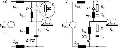
FIGURE 6.10 Snubber and switch equivalent circuit.
TABLE 6.1
Underwriters Laboratory (UL) Classification (Rating) of Low-Voltage Fuses
UL Class |
Fuse Overload Characteristics |
Rating [Amperes] |
AC Voltage [Rating] |
Available Ampere Ratings |
L |
Time-delay |
200,000 |
600 |
200–6000 601–4000 200–2000 |
RK1 |
Time-delay |
200,000 |
250 600 |
0.10–600 |
fast-acting |
200,000 |
250 600 |
1–600 |
|
RK5 |
Time-delay |
200,000 |
250 600 |
0.10–600 |
T |
Fast-acting |
200,000 |
300 600 |
1–1200 1–1200 |
J |
Time-delay |
200,000 |
600 |
1–600 |
Fast-acting |
200,000 |
600 |
1–600 |
|
CC |
Time-delay |
200,000 |
600 |
0.10–30 0.25–30 |
Fast-acting |
200,000 |
600 |
0.10 |
|
CD |
Time-delay |
200,000 |
600 |
35–60 |
G |
Time-delay |
100,000 |
480 |
0.50–60 |
K5 |
Fast-acting |
50,000 |
250 600 |
1–600 |
H |
Renewable fuses fast-acting |
10,000 |
250 600 |
1–600 |
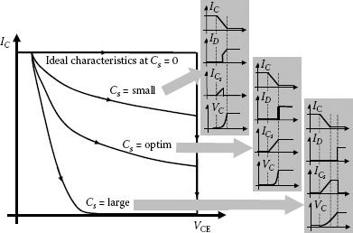
FIGURE 6.11 Discussion on the snubber capacitor value.
where I0 is the load current at the moment of turn-off. Replacing this solution in Equation 6.3 yields:
(6.5) |
One can define a maximum desired voltage across the IGBT [VMAX] and replace for the maximum defined by previous equation.
(6.6) |
Therefore, calculation of the needed capacitor value depends on the estimated value for the parasitic inductance.
Using the decoupling capacitor alone may not be the solution when the resonance between the DC link inductance and this capacitor produces a large bus ringing. An alternative solution is to insert a resistor-diode circuit in series with the capacitor. This will clamp the ringing. When the switch turns-off, the energy stored within Lp3 is transferred to the capacitor Cs. The tendency of returning the energy to the bus inductance through oscillation is blocked by diode Ds. Moreover, the capacitor is decoupled during turn-on and the DC link parasitic inductance will smoothen the turn-on transition and reduce the appropriate switching loss. The drawback of this approach is the additional inductance introduced in the circuit by the resistor–diode connection.
For high-power applications, the solution presented in Figure 6.10b is used. The snubber contains an Rs–Cs series network across each power semiconductor switch.
The Cs capacitance must be twice as large as the parasitic capacitance of the power semiconductor switch and its mounting. The Rs resistor is introduced to sustain the whole load current when Cs is discharged.
Accordingly, it yields Rs = VDC/IL
A second condition for Rs can be derived from the time constant for the discharging process. The snubber capacitor should discharge back to VDC before the next turn-off moment, that is:
(6.7) |
The introduction of this resistor reduces the system efficiency due to inherent losses. The resistor loss at turn-off yields:
(6.8) |
Losses at turn-on can be approximated as having the same value.
Using a resistor–diode assembly for dumping the voltage ring is another option. Advantages in this case are similar to those for clamping of the whole DC bus. The snubber capacitor is fully discharged during IGBT turn-on, whereas it is fully charged at turn-off. The losses in the snubber resistor are substantially higher in this case and can be expressed as
(6.9) |
Snubber capacitors are subject to high peak and RMS currents as well as large dv/dt. The industry now provides capacitors especially built for this application. Snubber capacitors can be purchased as discrete components or as modules that allow connection of the snubber directly across the IGBT module terminal in order to minimize the terminal inductance. Table 6.2 presents different solutions for snubber capacitors provided by Cornell-Dubilier [9].
The snubber resistor should be selected to have the lowest possible inductance. Possible choices are carbon composite or metal film, but these are not easily available at high power. In this case, low inductance wire-wound resistors can be selected.
The diode in the snubber circuit experiences the same peak voltage as the snubber capacitor: the current is small in average but large in its peak. The blocking action of these diodes should be faster than the actual protected power semiconductor. Fast-switching diodes rated for the snubber capacitor voltage and circuit peak current should therefore be selected.
6.2.5.3 Undeland Snubber Circuit
Using Resistance-Capacitance-Diode (RCD) snubbers for both power semiconductor switches on one inverter leg requires many components and introduces large losses, as demonstrated. A special snubber circuit has been proposed by Undeland (Figure 6.12) to minimize the number of components and to reduce the losses within the snubber. This circuit confines all losses in only one resistor, simplifying the energy recovery.
TABLE 6.2
Solutions for Special Snubber Capacitors
Capacitor Cs2 separates the snubber circuit from the power stage during the intervals between switchings. At the end of each switching cycle, the excess energy within the inductance is discharged through Ds2 and Ds1 into the capacitor Cs1. The voltage across this capacitor tends to go above the DC bus voltage and the difference is dissipated on the snubber resistor Rs. This energy through Rs can be further recovered into the DC bus with regenerative snubbers.
6.2.5.4 Regenerative Snubber Circuits for Very Large Power
The higher the power within the power stage, the higher the losses in the snubber resistors associated with the six switches. For this reason, high-power converters are built with circuits able to recover something from this energy into the DC bus [10,11]. They are generally referred to as regenerative snubbers (Figure 6.13) [12,13,14].
It is worth noting that regenerative snubbers are useful in high-power converters equipped with slow-switching devices like gate turn-off thyristors (GTO) where losses are large. Such equipment is still in use in many places and some companies are currently producing GTO-based converters in multi-MW range. On the other hand, modern power semiconductor devices, for instance, IGBTs, are nowadays available in 1 kA range, and some of these devices do not need snubbering at all. Building snubberless power converters with IGBTs like Powerex MegaPack (300 V, 1000 A) makes this topic obsolete. However, due to historical reasons and due to the large number of GTO-based converters in use, regenerative snubbers are presented here.
The whole idea of using a snubber circuit can be reduced to controlling the slope of the current increase at turn-on and the slope of voltage at turn-off. The most minimal solution has been shown to be a series inductor for turn-on and a parallel capacitor for turn-off. Complete solutions including resistance and diodes have been explained. Another concept is that of keeping all the transition losses out of the power semiconductor device by controlling its switching at zero current or zero voltage. This concept was first developed in the 1980s and is called resonant snubber. The simplest implementation of this concept consists of a circuit with a capacitor parallel to the power semiconductor device and an increased inductance in series (Figure 6.14).
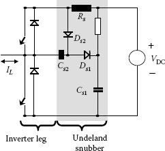
FIGURE 6.12 Undeland snubber with reduced losses.
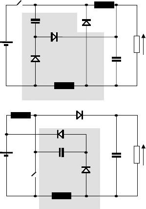
FIGURE 6.13 Circuit examples of regenerative snubbers.
This is represented as a buck converter, but it can also be a part of a converter leg. The capacitor might be the parasitic capacitor across a MOSFET device. The power semiconductor switch Sw1 will have transitions at zero voltage due to the resonance. It is controlled like regular switches within the buck or inverter leg operation.
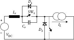
FIGURE 6.14 Principle of resonant snubber.
Supposing Sw1 is off, the load current IL is passing through Cr and Lr charging the capacitor. Assuming a constant current IL, the voltage across the resonant inductor stays zero while the capacitor voltage increases linearly.
(6.10) |
By difference, the voltage across D2 decreases as
(6.11) |
Shortly, this diode turns-on and the charging time interval is defined as
(6.12) |
It is important to note that the slope of the voltage increase across the switch Sw1 is ideally limited by resonance at IL/Cr. The existence of the time interval t1 does not considerably change the operation of the converter.
Next, the diode D2 conducts a part of the load current, while the rest of the current circulates through the series resonant circuit Lr−Cr. The voltage across the capacitor Cr is the solution of the differential equation:
(6.13) |
with as initial condition.
The expression of the capacitor voltage yields:
(6.14) |
This shows an increase of the capacitor voltage after turning-on the diode D2 and then a decrease toward zero according to the resonant swing. The capacitor voltage crosses zero only if:
(6.15) |
which is a very strong constraint for sinusoidal inverters. For small load currents, the voltage across capacitor will not cross zero. The current variation through Lr and Cr is a cosine function during this time. The moment of time corresponding to zero capacitor voltage is given by
(6.16) |
After this moment, diode D1 turns-on and takes over the Lr current and the Cr is no longer conducting current. The voltage across the inductor Lr is clamped at VDC and its current goes linearly to zero. Throughout this interval of current decrease, the voltage across Sw1 is kept at zero, and any turn-on command produces commutation at zero, voltage after the Lr current goes to zero. The time associated with this event is given by
(6.17) |
The duration of the OFF interval is thus limited by parameters of the resonant circuit:
(6.18) |
It can be noticed that power semiconductor devices are switched at zero voltage without switching losses. After Sw1 turns-on, current through Sw1 increases slowly due to Lr under a constant voltage VDC. Diode D2 stays in conduction for another short time interval under the same equivalent circuit derived previously during the D1 conduction. This interval ends when the current through D2 gets to zero. This current equals the difference between the load constant current IL and the linearly increasing current through Sw1.
A complete solution is presented in Figure 6.15 for a three-phase inverter. The capacitors are distributed in parallel with each switch, while the inductance is placed on the DC bus and increased from the value of the parasitic inductance. Modern MOSFET-based inverters can take advantage of the MOSFET’s inherent parallel capacitance. After the parasitic inductance is estimated, additional inductance may become necessary to achieve the desired resonant frequency. The resonant frequency influences the voltage swing slope and the delay to zero crossing.
The early 1990s brought the explosive development of IGBTs and this concept has been widely developed in what we know today as resonant converters. A special chapter is later dedicated to this topic.
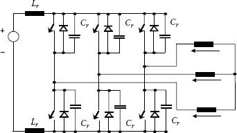
FIGURE 6.15 Distributed resonant snubber.
Voltage overshoot protection can also be achieved by including an additional stage in the gate driver (Figure 6.16) [15]. At turn-off, the protection transistor Qp is turned-on and the gate is discharged through it. When the IGBT collector voltage reaches the breakdown voltage of the Zener diode, a current flows through the gate of Qp and turns it off. The remaining current flows through Roff, slowing down the dv/dt rate. An additional benefit of this method is that switching power is reduced by half.
Another possible fault can occur at the gate-driver level. A faulty operation of the gate driver leading to absence of the control pulses at the IGBT gate should be detected and all the six gate drivers of the inverter turned-off. This is generally processed through the control device, a field programmable gate array (FPGA) or a digital signal processor circuit.
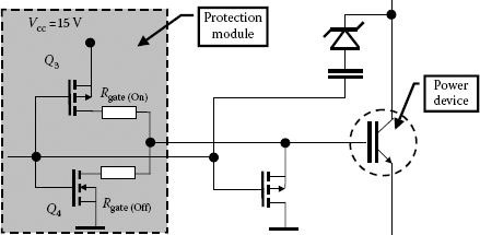
FIGURE 6.16 Active voltage overshoot protection.
6.3 SYSTEM PROTECTION MANAGEMENT
Complex systems including multiple power converters, sources, or loads have a protection system that sets several levels of priority for communication between them. This is also discussed in Chapter 7 [16].
6.4 REDUCTION OF COMMON MODE EMI THROUGH INVERTER TECHNIQUES
Chapter 1 has shown the importance of preventing common- and differential-mode electro-magnetic inference (EMI) in switching power converters and the appropriate standards have been described. Special EMI filters are commercially available for currents up to 100 A in grid-connected applications. They are based on higher order passive filters especially calibrated to limit EMI according to standards.
Let us now take a look at some circuit solutions for the common-mode EMI reduction. Three-phase inverters in which the neutral is not connected experience a continuous variation of the neutral voltage with respect to earth. This is illustrated in Figure 6.17 for a pulse width modulation (PWM) algorithm that represents a sequence of active and zero states already known for the three-phase inverter.
Each state of the inverter operation produces a different level of neutral voltage as shown in Table 6.3. The largest neutral voltage change (step) occurs when using zero states. A possible minimization of the common-mode voltage and ground current can be achieved by avoiding zero states within the PWM generation [17,18]. The drawback of such a solution is in increasing the ripple of the motor currents and limiting the maximum modulation index.
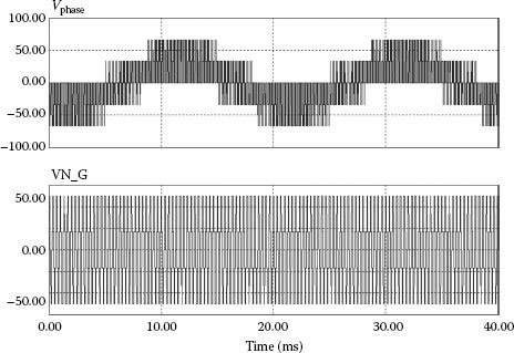
FIGURE 6.17 Variation of the neutral point voltage in respect with the middle point of the DC link for a Sinusoidal PWM at 3 kHz and VDC = 100 V.
TABLE 6.3
Neutral Voltage for Each State of Inverter Operation
[1 0 0] |
–0.16 * VDC |
[1 1 0] |
0.16 * VDC |
[0 1 0] |
–0.16 * VDC |
[0 1 1] |
0.16 * VDC |
[0 0 1] |
–0.16 * VDC |
[1 0 1] |
0.16 * VDC |
[1 1 1] |
0.50 * VDC |
[0 0 0] |
–0.50 * VDC |
The parasitic coupling between the neutral point of the load and ground creates a path for the common-mode current flow. Note that the slope of neutral point voltage variation follows the voltage variation across the power semiconductor switches. The faster are these switchings, the larger is the current to ground. Figure 6.18 shows the capacitor path of the common-mode current.
Capacitor Cg can be the machine’s stray capacitance or the distributed parasitic capacitance to ground. These common-mode currents create EMI problems and can produce damage to the electrical machine through bearing current, shaft voltage, insulation breakdown, or current flowing through the stray capacitors between motor and frame. These currents show components within the range of 100 kHz to tens of MHz and cannot completely be removed with ordinary chokes or EMI filters (like baluns).
A prior solution considered a common-mode transformer with an additional winding shorted by a resistor (Figure 6.18) [19,20,21]. The neutral point voltage is detected with an RC three-phase network. In this solution, care has to be taken to choose the appropriate R and C components, as they appear in parallel with each load phase. One improvement is to create the neutral voltage with an iron core transformer that offers very large impedance in parallel with each load phase (Figure 6.19). The resulting current circulates through the fourth winding of a four-winding ferrite-core common-mode inductor [22]. This is used for common-mode current cancelation. Furthermore, an RC circuit is used (Figure 6.19) to limit the power dissipation, as only the edges of the common mode voltage are addressed in order to minimize their slope.
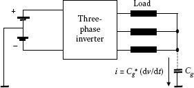
FIGURE 6.18 Common mode current.
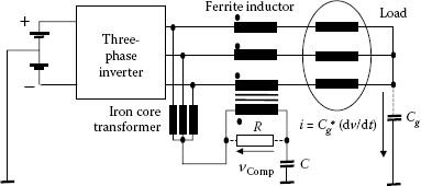
FIGURE 6.19 Common mode transformer.
This group of methods has proven inefficient in withdrawing the aperiodic ground-current. Elimination of both oscillatory and aperiodic ground currents (common-mode voltage) have been attempted with active circuits [21,23]. They can be used in the horsepower range in which high-frequency transistors are available for common-mode voltage control. One of these solutions is shown in Figure 6.20 [24]. The common-mode voltage at the inverter output is reconstructed with a set of small capacitors Cx and used to control an inverter leg. This adds a compensating voltage at the inverter outputs through the transformer Tr. This completely cancels the common-mode voltage on the load.
The implementation issues of this method relate to the choice of the transistors in the active circuitry. Transistors are operated in the active region following emitters and should have a wide frequency bandwidth and low output impedance to eliminate any influence of the output current in the compensating voltage. The high-frequency bandwidth ensures that the compensating voltage precisely follows the slopes of the inverter output voltages. The power dissipation within these transistors is very small (~0.5%) as the transistors carry only the transient part of the load voltage.
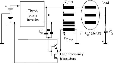
FIGURE 6.20 Active control with high frequency bandwidth transistors.
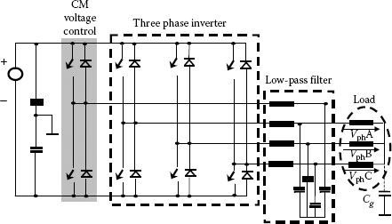
FIGURE 6.21 Four leg inverter.
At high-power levels, none of these approaches based on active common voltage canceling is convenient [25]. The alternative solution consists in using a fourth converter leg (Figure 6.21).
The power converter becomes a converter with four identical legs followed by LC low-pass filters. For balanced systems, the fourth leg can be derated with respect to the conventional inverter. The role of this additional leg is to complement the neutral voltage so that the instantaneous sum of all pole voltages is zero and no common-mode current is created. The drawback is that it is not practical to add a fourth load phase for the compensating current. A filter system with four phases can be used to fictitiously create the fourth phase and cancel common-mode voltage at the neutral point. If the load is perfectly symmetrical, this idea works perfectly. It is limited only by the frequency characteristics of the transfer function through the passive components used in filter and load.
Summation of voltage effects is therefore created through the low-pass filters LC when the fourth leg voltage is generated by reversing the information from Table 6.2, that is, to have always two switches tied to the positive DC rail and two switches to the negative rail. However, zero states cannot be used within this approach. Other PWM algorithms can however be defined without the use of zero states. A possible solution is to create the effect of zero state by employing two opposite vectors. For instance, if the last active state before the zero state was [1 0 0], we create the effect of the zero state by using the active states [1 0 0] and [0 1 1], each for half of the time desired for the zero state. Figure 6.22 illustrates this principle for a single pulse within the PWM algorithm. The extended time intervals associated with the active states produce more ripple on the load phase currents. In other words, a proper selection of the PWM algorithm can help in reducing the common-mode voltages at the price of increased ripple on the load.
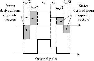
FIGURE 6.22 PWM without zero states.
6.5 TYPICAL BUILDING STRUCTURES OF THE CONVENTIONAL INVERTER DEPENDING ON THE POWER LEVEL
As shown in Chapter 1, the same circuit topology can be used at 10 or 1000 A, but building the appropriate power converters differs with the power level. In order to understand constraints for packaging power converters at different power levels, let us start with a review of power semiconductor packages.
6.5.1 PACKAGES FOR POWER SEMICONDUCTOR DEVICES
Figure 6.23 illustrates different packages used for IGBT devices. For currents of tens of amperes through-hole packages, such as TO-220 and TO-247, are preferred for power semiconductor switches. They are used with printed circuit boards (PCBs) to build power converters below 40 A. This direction toward use of PCBs has been imposed by power converter manufacturers for cost reasons and to take advantage of the existing PCB-automation tools. These packages benefit from putting both the power semiconductor switch and the associated diode within the same package and offering it at very low cost per ampere. For instance, a 20 A/600 V IGBT/diode can be found under $1.50 in a single component order, and a 60 A/600 V IGBT for less than $5.00 for a single component order (digikey data shown for Fall 2012).
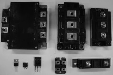
FIGURE 6.23 IGBT packages.
For low- and medium-power applications, IGBTs are packaged in dual (inverter leg) or six-pack assemblies. Unfortunately, the packaging is not consistent from one manufacturer to another and it is similar to the former bipolar Darlington power modules.
Modern power modules also include control and protection circuitry within the same package in order to simplify the inverter building and reduce costs of auxiliary parts. There is no standard for these intelligent power modules and they are not interchangeable as characteristics, control, or protection. This becomes a serious limitation to paralleling such modules. Single inline package (SIP) and dual inline package (DIP) modules are another alternative for power modules used in low power appliances. Given the wide emergence of these devices over the last years, a special chapter is later on dedicated to their presentation.
Different manufacturers have tried during the last years to provide standard packages, especially for the low-power market where power converter manufacturing is based on more automation. The EconoPACK (Figure 6.24) and EconoPIM modules are dedicated packages below 20 kW (1200 V, 100 A) and contain a full bridge with through-hole terminals able to connect the control circuitry from a PCB. Above 100 kW, integrated hybrid modules (IHM) modules are used.
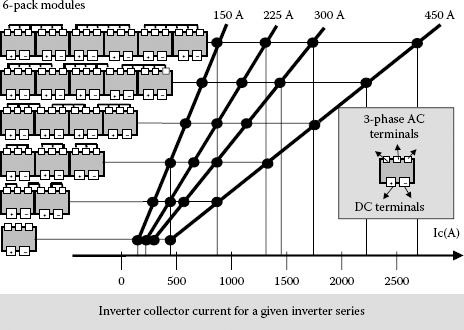
FIGURE 6.24 Packaging for Parallel applications: EconoPACK+.
Because a power converter manufacturer generally has to address a wide power range and provide very large volumes at lower power levels, a new approach has won market share during the last few years. The packaging has been changed to accommodate easy paralleling of power modules to define a very large power range that can be easily manufactured. The major features are:
• Define a flow-through concept by separating the power DC terminals on one side and phase output terminals on the other.
• Parallel the three legs of a six-pack IGBT if and when necessary.
• Use the same housing for dies that support currents from 150 to 450 A in order to achieve easy scaling of heatsinks, bus bars, and drivers.
At higher currents, the IGBT modules are mounted directly on heatsinks or cold plates while the electrical terminals are connected through screws on top to special structures called bus bars.
In the medium-power range, there is always a temptation to save money by paralleling multiple low-power IGBTs packaged in TO-220 or TO-247 packages. However, such an approach loses the advantages of the PCB mounting and requires high-current wiring of all semiconductor power terminals.
All of these higher power modules are more expensive. For instance, a 300 A/600 V dual (half-bridge) IGBT can be purchased under $150 in a single component order, a 600 A/1200 V dual IGBT under $400 in a single component order; while the largest in family, the 1400 A/1200 V dual IGBT can be found under $1000 (digikey data shown for Fall 2012). It is important to understand that the cost of a module is mostly dependent on the mechanical packaging and not on the size of the semiconductor die that is inside. This is why the cost becomes advantageous if the package accommodates the largest semiconductor die that it can.
In the very high-power range, IGBTs are packaged as discrete devices only.
Once the power semiconductor devices have been selected and the size and terminals of the appropriate module have been understood, the next element to look at is the converter packaging. It has been mentioned that PCBs are the best solution below 40 A. Multilayer PCBs allow large currents on different isolated layers. They are suitable for power devices with through-hole terminals.
At higher currents, there are two options for power distribution:
• High current (heavy-gauge) wires: Heavy-gauge wires can be used at reasonable power levels but they introduce difficult routing and bending within the converter enclosure.
• Copper bus bars with tapped holes for cable connection. Copper bus bars are built in different sizes and can carry current in a simple, reliable way. They should be several inches apart from each other and be isolated from the cabinet by fiberglass reinforced plastic spacers.
An alternative solution has been recently introduced that uses laminated bus bars built of a multilayer structure of copper and dielectric insulator. They were first used in computer and telecommunications systems, but were introduced recently in medium- and high-power converters (Figure 6.25). The advantages of this technology is better cooling, lower resistance than wires (lower voltage drop), minimized stray inductance (lower voltage overshoots), and the possibility to use different copper layers in the laminated package for different purposes. For instance, a direct comparison of a connection with twisted wires and one with a laminated bus bar shows half DC resistance of the new solution (0.006 versus 0.0032 Ω), and a substantial decrease in the high frequency impedance at 1 MHz from 0.078 to 0.019 V. Using each layer for another function highly improves packaging of power converters for modern requirements up to 1000 A or 5000 V [26].
Due to their ruggedness, they can also be used as mounting platforms for auxiliary components, such as protection circuitry breakers or snubbers [27]. Moreover, special structures are built for IGBT devices or modules to accommodate their terminals (Figure 6.25).
After the electronics has been packaged and assembled together, the entire equipment should be placed inside an enclosure. Enclosures are defined by NEMA standard ICS 1-110 [28] as
• Type 1 is a general purpose enclosure, useable indoor, aiming at personnel protection and water dripping inside the electronic circuitry.
• Type 4 is a watertight, dustproof, nonventilated indoor or outdoor enclosure.
• Type 12 is a dustproof, driptight, indoor enclosure.
Usually, enclosures are built with steel of Gauge 10-12, occasionally with Gauge 14. All doors should have safety closing. Freestanding enclosures should be under 90 inches.
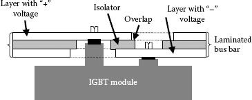
FIGURE 6.25 Possible use of a laminated bus bar at IGBT module connection.
The IP Code (Ingress Protection Rating) [29] provides another classification and rates the degree of protection provided against the intrusion of solid objects (including body parts like hands and fingers), dust, accidental contact, and water in mechanical casings and with electrical enclosures. IP codes have the format IPxx, where the xx represent numerals from the coding scheme. The first number in the sequence signifies the degree of protection against the entry of foreign solid objects (0 = not evaluated; 1 = for greater than 50 mm diameter; 2 = for greater than 12.5 mm diameter; 3 = for greater than 2.5 mm diameter; 4 = for greater than 1 mm diameter; 5 = dust protected; 6 = dusttight). The second number signifies the degree of protection against the entry of moisture and may be anything from 0 through 8 (0 = Not evaluated; 1 = Dripping water: from vertical; 2 = Dripping water: at 15° tilt; 3 = Spraying water; 4 = Splashing water; 5 = Jetting water; 6 = Powerful jetting water; 7 = Temporary immersion; 8 = Continuous immersion). Test procedures generally accompany the actual rating for a better understanding of the enclosure’s capabilities.
Enclosure cooling is done by radiation and convection. Reference [28] provides empirical relationships for estimation of temperature rising, for an ambient under 50°C:
Radiation
(6.19) |
Convection
(6.20) |
In the first cases, η = emissivity (Table 6.4).
TABLE 6.4
Radiation Emissivities for Certain Materials
Material |
Emissivity |
Polished silver |
0.02 |
Polished aluminum |
0.05 |
Polished brass |
0.60 |
Copper |
0.15 |
Oxidized steel |
0.70 |
Cast iron |
0.25 |
AL paint |
0.55 |
Black gloss paint |
0.90 |
White lacquer |
0.95 |
White enamel |
0.95 |
The numerous gate driver circuits as well as the current and voltage sensing circuitry need isolated power supplies. If the gate drivers for lower power converters (HP range) can be simply supplied through bootstrap power supplies, dedicated power supplies are necessary at higher power levels.
The number of these isolated power supply channels can be very high. For instance, a conventional three-phase inverter may require a supply of 6 gate drivers, a bipolar voltage for the phase current measurement circuits, one for the measurement of the DC bus voltage, a 5 V or 3.3 V for the digital control circuitry, and possibly some voltages for isolated communication channels. The internal power distribution system hence becomes very complex.
In order to reduce the component count and to maintain the system’s efficiency quite low, the flyback converter topology is mostly used. It is the simpler possible one-switch converter, allowing generation of multiple secondary side voltages. Since the regulation is in general done on only one channel of secondary voltage, the different supply voltages may have weaker regulation than expected. If this is the case, the regulation can be improved further with local nonisolated voltage regulators.
The control of the flyback power supply as well as the control of any other low voltage PWM type voltage regulator can be achieved with a family of integrated circuits that follows the original design of Bob Mammano.
The introduction of the PWM control IC is an excellent example of disruptive innovation. This integrated circuit has been invented by Bob Mammano [30] in 1975, and introduced to market in 1976 by Silicon General Company, as SG1524. In 1970s, similar PWM Control ICs (Figure 6.26) were developed by multiple corporations like Motorola MC3420, Texas Instruments TL454, Signetics NE5560, Ferranti ZN1066, Fuji FA553 [32].
The IC is based on a mixed-mode IC technology with a very simple structure, well-known today. Its apparition coincides with the advent of switching power supplies in late ’70 s and it did satisfy a clear market need, able to add value to the customers. It also helped the creation of a new market through an interesting paradigm (vendors competing customers). It did enable new power supply technologies and subsequently a more incremental development. Circuits like current mode ICs, cycle-by-cycle current limiting protection, single-ended, push-pull supplies, LDOs, hot-swap, soft-switching, so on, have benefited from the original PWM chip idea.
Today, the power control IC industry has a market of more than $5 billion.
As the technology substrate has developed, additional features were incorporated along the conventional PWM control with current regulation. Some of such features are next listed:
• Advanced soft-start
• Quasi-resonant flyback
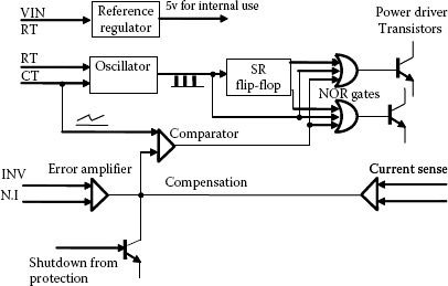
FIGURE 6.26 Structure of the PWM control IC.
• Valley switching for low EMI
• Stand-by power requirements
• No-load power requirements (like < 300 mW no-load power)
• Current-mode control
• Multimode power saving with automatic switching between operation modes
• Pulse skipping, or pulse density modulation
• Burst operation, up to hard-switching
• Green mode status indicator (can disable PFC)
• Both line and load over-voltage protection
• Bounded frequency range, with frequency foldback
A derivative product was the PWM control chip for the flyback power supplies. It is the most used class of ICs for isolated power supplies, featuring the entire controller in a 8-pin package. The history of the original Unitrode products was marked by the following milestones:
• 1980s—Introduced as UC3842: simple structure, 144 transistors, in 7.5 mm technology, sold for $1.75.
• 1990s—Feature improvement: sold as UCC3802, 478 transistors, in 3.0 mm technology, sold for $0.85.
• 2000s—More features: sold as UCC38600, 1158 transistors, in 0.5 mm technology, sold for $0.45.
The application circuitry is illustrated in Figure 6.27 for the case of a single secondary. Similar designs can consider the generation of multiple secondary voltages while using a single control IC.
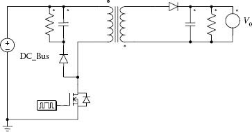
FIGURE 6.27 Single-switch flyback power supply.
6.6.3 OPERATION OF a FLYBACK POWER CONVERTER
Depending on the conduction state of the power MOSFET, there are two operational states of the circuit. When the switch is ON, the secondary side diode becomes reverse polarized and turns-off. The MOSFET device allows a current circulation through the primary winding, and the inductor core flux increases linearly from its initial value.
(6.21) |
After a conduction time interval ton, the power MOSFET turns-off and the energy stored in the core causes the current to flow in the secondary side, through the diode D. The voltage across the secondary winding becomes [−V0], and the flux decreases linearly:
(6.22) |
(6.23) |
For a steady-state operation, the final value should be equal to the initial value for the next cycle:
(6.24) |
Hence:
(6.25) |
The duty cycle yields:
(6.26) |
This calculation has followed a similar approach with a buck-boost converter. However, the operation of a flyback power converter may be influenced by discontinuous mode of operation (DCM), when the equations become more complex. The output voltage will also depend on the load in such case (Figure 6.28).
While operated in DCM, the entire energy is transferred to the load and the duty cycle depends on the load energy, input voltage, and inductance value:
(6.27) |
where VDC is the input voltage.
It is important to note that the control of energy is assured during the ON-time of the primary-side MOSFET, while the energy is delivered to load during the OFF-time. This means there is no control possible during the time the energy is actually transferred to load. If the converter operates in CCM, the energy accumulated in inductor will be delivered to the load uncontrolled over several cycles, before an action can be done by control. This behavior is also seen in the small signal model as a right-half-plane zero. The phase decreases with increasing gain, and this must be considered when defining the control-loop compensation. The general rule for converters with a right-half-plane zero is to design at the lowest input line voltage and at the maximum load current, restricting the bandwidth of the feedback loop to about one-fifth the right-half-plane zero frequency. The right-half-plane zero frequency for CCM yields as
FIGURE 6.28 Typical waveforms for the operation of a flyback power converter in discontinuous conduction mode.
(6.28) |
The same behavior of right-half-plane zero is also seen in DCM. However, this is usually not a problem anymore as the frequency moves above half of the switching/sampling frequency.
A final comment about the control system relates to the actual use of the flyback power supply within a multiphase power converter. In such application, there are multiple secondaries of the flyback transformer required to power multiple low voltage circuits with galvanic isolation. These loads have variable currents and it is virtually impossible to regulate all voltages at a while. The compromise is usually to set the feedback loop after the most restrictive secondary that is usually the supply of digital circuitry. Additional solutions require small on-board 3-pin voltage regulators on each secondary for precise regulation without isolation. However, the gate drivers and some current, temperature and voltage sensing devices (connected in differential mode) do not require accurate regulation of voltage.
The latest flyback control ICs benefit from the following features [31,32]:
• Operation with variable frequency to maintain discontinuous or boundary (also called transition mode) conduction modes with advantages in
• Efficiency optimization (operation with diode turn-off by zero current is virtually lossless, with no diode reverse recovery, and it improves efficiency)
• Smaller size of the flyback transformer given the requirement for a smaller inductance
• Small-signal modeling, with the plant model reduced at a first order model for either voltage-control mode or current control mode
• Operation in “green mode”, where the PWM sequence is shut-down at low load, with a burst mode operation
• Special protection features like over-voltage detection, maximum ON-time programming, fast latch-up fault recovery, and thermal shutdown
There is disadvantage of higher peak current when operated in DCM or BCM, with bad influence in EMI, MOSFET conduction loss, over-voltage protection. However, the cost difference of using a higher current MOSFET is minimal and the problems are thus solved.
Despite being the most critical design component, the actual design and construction of a flyback transformer is beyond the scope of this book as flyback transformer can be acquired off-the-shelves or by order with system-level requirements.
This chapter presents details related to the building of a three-phase power converter. Information about three-phase power converters can easily be found in many textbooks, but the way the converter is built and protected is also important. Modern techniques have been shown to improve performance criteria such as efficiency, power density, and input or output harmonics.
P6.1 |
A 24V/120V boost converter is built with an IGBT and a diode switched at 20 kHz. The IGBT is protected with a snubber capacitor. The parasitic inductance of the circuit is 10 nH, the maximum input current is 100 A and a voltage increase of maximum 5% is allowed. Estimate the required snubber capacitance. |
P6.2 |
Select a resistor to form an RC snubber circuit for the previous converter. Calculate losses within the resistor. |
P6.3 |
Consider a single-phase IGBT inverter with snubber circuits across each IGBT. The DC voltage is 270 V, switching frequency is 16 kHz, maximum current is 120 A and a voltage overshoot of 10% is allowed. The bus parasitic inductance has been estimated at 20 nH. Define the values for the resistor and capacitor and estimate resistor power losses. |
P6.4 |
Explain how an RC network connected in parallel with the load would serve as a turn-off snubber for all 4 IGBTs in the previous problem. Calculate values of components within such network and estimate power losses. Why the solution of previous problem is more preferable? |
P6.5 |
Rewrite the SVM time equations for |
P6.6 |
The common mode current is produced by derivative of the neutral voltage. This current is lower for PWM algorithms that do not produce large variations of the neutral point voltage. Considering Table 6.3 along with the switching sequences considered in the previous Chapter for the SVM algorithms, determine which state sequence produces the lowest peak-to-peak common-mode current. |
P6.7 |
Draw for each sequence the qualitative evolution of the common mode current. What is the frequency of the most important component? |
P6.8 |
A buck converter built with an IGBT and a diode is switched at a frequency fsw with a constant duty cycle producing an on-state loss of 100 W and a switching loss given by 0.01 * fsw. The maximum junction temperature of the IGBT is 150°C and the junction-to-case thermal resistance is 2°C/W. The cooling system maintains a quasi-constant case temperature at 60°C. What is the maximum allowable switching frequency. |
P6.9 |
Consider the same IGBT mounted on a heatsink while the ambient temperature is 27°C. Consider a switching frequency of 16 kHz and calculate what is the maximum heatsink thermal resistance. |
1. Mohan, N., Undeland, T., and Robbins, W. 2002. Power Electronics. 3rd edition. John Wiley and Sons, New York.
2. Cline, C. 1995. Fuse protection of DC systems. Annual Meeting of the American Power Conference.
3. Anonymous 2002. Semiconductor Fuse—Application Guide. Ferraz-Shawmut Corporation, January.
4. Anonymous 2002. Introduction to Power Electronics and Protection Methods. Ferraz-Shawmut Corporation, January.
5. Severns, R. 1997. Design of snubbers for power circuits. PCIM.
6. Zhang, Y., Soghani, S., and Chokhawala, R., 1995. Snubber considerations for IGBT applications. IRF Design Tip Documentation
7. Severns, R. 2008. Snubber Circuits for Power Electronics, Ed.
8. Iov, F., Blaabjerg, F., and Ries, K. 2003. Prediction of harmonic power losses in fuses located in DC-link circuit of an inverter. IEEE Trans. IA 39(1), 2–9.
9. Anonymous 2004. Cornier-Dubilier Databook. Documentation. Chicago, IL
10. Thiyagarajah, K., Ranganathan, V.T., and Ramakrishna, R.M. 1991. A high frequency IGBT PWM rectifier/inverter system for AC motor drives operating from single phase supply. IEEE Trans. PE 6(4), 576–584.
11. Deacon, J.H., Van Wyk, J., Schoeman, J. 1999. An evaluation of resonant snubbers applied to GTO converters. IEEE Trans. IA 23(2), 292–297.
12. Steyn, C. and Van Wyk, J. 1989. Optimum nonlinear turn-off snubbers: Design and applications. IEEE Trans. IA, 25(2), 298–304.
13. Swanepoel, P.H. and Van Wyk, J.D. 1994. Analysis and optimization of regenerative linear snubbers applied to switches with voltage and current tails. IEEE Trans. PE 9(4), 433–442.
14. Steyn, C. 1989. Analysis and optimization of regenerative snubbers. IEEE Trans. PE 4(3), 362–370.
15. Heath, D. and Wood, P. 1999. Overshoot voltage reduction using IGBT modules with special drivers. IRF Design Tip Documentation.
16. Donescu, V. 2001. Fault detection and management system broadcasts motor drive faults. PCIM, June.
17. Cacciato, M., Consoli, A., Scarcella, G., and Testa, A. 1998. Continuous PWM to square-wave inverter control with low common mode emissions. IEEE PESC, pp. 871–877.
18. Holmes, DG. 1996. The significance of zero space vector placement for carrier based PWM schemes. IEEE Trans. IA 32(5), 1122–1129.
19. Ogasawara, S. and Akagi, H. 1996. Modeling and damping of high frequency leakage currents in PWM inverter-fed AC motor. IEEE Trans. IA 32(5), 1105–1114.
20. Swamy, M.M., Yamada, K., and Kume, T.J. 2001. Common mode current attenuation techniques for use with PWM drives. IEEE Trans. PE 16(2), 248–255.
21. Ogasawara, S., Ayano, H., and Akagi, H. 1998. An active circuit for cancellation of common mode voltage generated by a PWM inverter. IEEE Trans. PE 3(5), 835–841.
22. Shimizu, T., Kimura, G. 1996. High frequency leakage current reduction based on a common mode voltage compensation circuit. IEEE PESC, pp. 1961–1967.
23. Pelly, B. 2002. Active common mode filter connected to the AC line. Patent application No. 20020171473, November 2002.
24. Oriti, G., Julian, L., and Lipo, T.A. 1997. An inverter/motor drive with common mode voltage elimination. IEEE IAS, Conference Record, vol. I, pp. 587–592.
25. Julian, L., Oriti, G., and Lipo, T.A. 1999. Elimination of common mode voltage in three-phase sinusoidal power converters. IEEE Trans. 14(5), 82–989.
26. Whistler, R.J. 1999. Laminated bus bars eliminate unmanageable cabling in high power systems cabinets. PCIM Magazine, June 1999, pp. 1–4.
27. Dimino, C.A., Dodballapur, R., Pomea, J.A. 1994. A low inductance simplified snubber power inverter implementation. Proceedings of the HFPC, April.
28. Sueker, K. 2005. Power electronics design. Newnes Ed.
29. Bisenius, W.S. 2012. Ingress protection: The system of tests and meaning of codes. Compliance Engineering Magazine, www.ce-mag.com.
30. Mammano, B. 2007. A historical perspective of the power electronics industry, plenary session. APEC.
31. Picard, J. 2010. Under the hood of flyback SMPS designs. 2010 Texas Instruments Power Supply Design Seminar, SEM1900, Topic 1, TI Literature Number: SLUP261, 2010.
32. Fujii, M., Maruyama, H. and Boku, K. 2002. FA5553/FA5547 series of PWM control power supply IC with multi-functionality and low standby power. Fuji Electr. Rev. 54(2), 68–72.
33. Pelly, B. 1994. Choosing between multiple discretes and high current modules. IRF Design Tip Documentation.