
Apart from the conventional use of IPM devices shown in Chapter 10, there are other topologies that also benefit from using these devices. The main idea behind the topologies presented in this chapter is to split the switched mode control into multiple power switches instead of using a higher power rated device. This was also analyzed in Chapter 14. Multiple switches allow us to introduce more control of the output waveform with benefits in reducing loss and improve reliability. Eventually this would emerge into a new set of high-performance topologies assembling a “network of switches.”
18.1 GRID INTERFACE FOR EXTENDED POWER RANGE
The first chapter of this book has presented standards for harmonics within the grid current that stand true independent of the power electronics topology used for energy conversion. The desire to reduce the packaging complexity of the power electronics equipment with the use of Intelligent Power Modules applies also to grid interfaces. Whilst the advent of IPM devices is noteworthy, their power levels tend to be limited. A novel power conversion principle is proposed in [1] to augment the power capability of an IPM device with a diode rectifier, or reversing the logic, to correct the harmonics of the input current within a diode rectifier by using an IPM device.
The conventional topology of an active power filter is considered as a starting point (Figure 18.1), and instead of dwelling into advanced control of current and power, the IPM hardware available on the market is herein used.
The power diodes within a diode rectifier conduct for 120° only, and there are 2 intervals of 60° on each phase without any current conduction. A current control algorithm is used to drive current into the grid from the three-phase power converter during such intervals only. The power to supply the three-phase power converter is taken from the load-side of the diode rectifier as a pure rectified voltage (Figure 18.2) and the references for the three phase currents follow Figure 18.3.
The current generated by the 6-switch power converter closes through the two conducting diodes and back to the power converter. This circulation will overload a little the diode rectifier. The current circulation though diodes improves the input (grid) current even if this is somewhat in an uncontrolled way, based on the offline current reference.
The current controller follows a feed-forward algorithm previously discussed in Sections 9.4 and 13.3.9.2 as well as in reference [2]. Synchronization with the grid voltage of the control system is very important herein for both the definition of the six operation modes, and the dead-time intervals shown in Figure 18.3. Each one of the six individual current controllers needs to achieve a fast locking to its triangular reference and to work after and/or before the others have started. Yet, their operation must start and finish after and respectively before the diodes have finished their switching of the current. Depending on the peculiar hardware, this may produce glitches in the resulting input current (see later on, Figure 18.6).
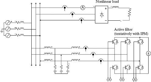
FIGURE 18.1 Conventional topology for an active filter.
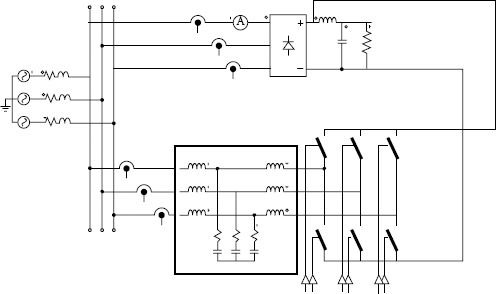
FIGURE 18.2 Novel hardware.
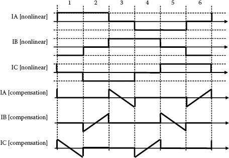
FIGURE 18.3 Theoretical current references for the novel method.
Figure 18.4 is showing individual current waveforms without passive filtering.
The two 60°-wide intervals when the 6-switch power converter influences the operation with the injection of triangular currents can be seen. During the remaining four 60°-wide intervals, the correction of the grid current yields from the circulation of the compensation current through the rectifier’s conducting diode, and a pulsed current superimposes to the traditional square-wave current. The waveforms of Figure 18.4 have a high content in fundamental, hence satisfying the grid harmonic standards.
Using a triangular current reference induces a light third harmonic (Figure 18.6).
The compensation power converter is rated in respect to the load power. The maximum peak current for the compensation converter is at 0.5578 of the load current (Figure 18.3). The power loss and thermal requirements are extremely beneficial since each IGBT works in switched mode for 1/6 of the period, under the line-to-line voltage, at a current ranging from −0.5578 to 0.5578 of the load current.
Let us calculate the power loss distribution for each IPM package in different circuit configurations (Figure 18.5). For comparison we will use data provided by manufacturer along its own loss calculation formulas, for the example of a back-to-back motor drive.
A. Conventional back-to-back motor drive (similar to data from manufacturer’s example)
System Data:
• Motor power rating 1 HP = 745 W A/C
• DC bus voltage Vdc = 400 V
• Modulation index of 0.8
• Line to line voltage VLL = 113 Vrms
• Power factor PF = 0.6
• Phase current Iph = 4 Arms
• Switching frequency fsw = 4 kHz
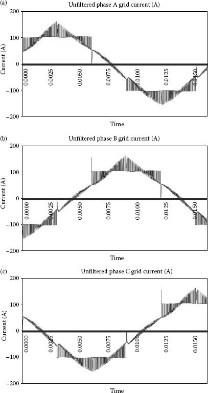
FIGURE 18.4 Grid phase currents (data samples printed with Excel).
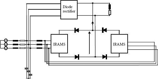
FIGURE 18.5 Implementation with IPM/IRAMS modules.
Power Loss Calculation:
• Pswitching (I + D) = 0.48 W
• Pcond, switch = 2.46 W
• Pcond, diode = 0.64 W
• Total Ploss per IPM module = 21.48 W
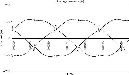
FIGURE 18.6 Currents calculated with moving average at 160 μs from samples in Excel.
B. New converter in active filter role (Figure 18.2), used along 25 A rectifier load
System Data:
Converter phase current Iph = 10 Arms
Load current in rectifier Irectifier = 25 Adc
Switching frequency fsw = 12.5 kHz
Power cycle = 0.33
Power Loss Calculation:
Pswitching (I + D) = 1.16 W
Pcond, switch = 1.11 W
Pcond, diode = 0.53 W
Total Ploss per IPM module = 16.80 W
C. New converter in active filter role (Figure 18.2), used along 50 A rectifier load
System Data:
Converter phase current Iph = 20 Arms
Load current in rectifier Irectifier = 50 Adc
Switching frequency fsw = 12.5 kHz
Power cycle = 0.33
Power Loss Calculation:
Pswitching (I + D) = 2.42 W
Pcond, switch = 1.46 W
Pcond, diode = 1.06 W
Total Ploss per IPM module = 29.64 W
Another demonstration of capabilities for this new converter topology and its afferent control is made for a direct comparison of power losses when a certain rectifier load current (DC) is produced. Basically, we are seeking the method able to generate the DC current with lower amount of losses overall. The following examples are using numeric data especially selected to produce around 30W power loss for different converter designs.
A. Direct three-phase IGBT 6-switch bridge producing a DC current of Irectifier = 6.5 Adc
System Data:
Iph = 5.0 Arms,
m = 0.8
Unity Power Factor:
fsw = 6.00 kHz
Power Loss Calculation
Pswitching (I + D) = 0.87 W
Pcond, switch = 3.42 W
Pcond, diode = 0.80 W
Total power loss Ploss per IPM module = 30.54 W
B. Conventional active filter for a rectifier load current of Irectifier = 20 Adc
System Data:
Iph = 22 Arms
Waveform = harmonic difference, conventional active filter definition
fsw = 12.5 kHz
Power Loss Calculation:
Pswitching (I + D) = 1.68 W
Pcond, switch = 2.99 W
Pcond, diode = 0.35 W
Total power loss Ploss per IPM module = 30.12 W
C. New method used for a rectifier load current of Irectifier = 50 Adc
System Data:
Iph = 20 Arms
Waveform = Figure 18.3
Power cycle = 0.33
fsw = 12.5 kHz
Power Loss Calculation:
Pswitching (I + D) = 2.42 W
Pcond, switch = 1.46 W
Pcond, diode = 1.06 W
Total power loss Ploss per IPM module = 29.64 W
In conclusion, this new control concept benefits from the intervals when diodes are not conducting current to inject a triangular waveform current that closes through the rectifying diodes, producing a natural compensation of the grid current. The results prove this method as an alternative to conventional grid interfaces as previously shown in Chapter 14. Using IPM devices allows a paradigm shift from conventional reasoning of saving or reducing the number of semiconductor components (Figure 18.5). Using IPM reduces the count of passive components, with advantages in size, weight, efficiency, and reliability.
Overall, one achieves a very low-cost solution, with a component minimized power stage, without additional power supplies or DC link capacitors, and a fully integrated electronics.
18.2 MATRIX CONVERTER MADE UP OF VSI POWER MODULES
18.2.1 CONVENTIONAL MATRIX CONVERTER PACKAGED WITH VSI MODULES
Considerable research effort has been dedicated to the three-phase AC/AC matrix converters [3,4,5,6,7,8,9,10,11,12] concerning both the realization of bidirectional switches and improving the PWM control. The operation and control of the conventional matrix converters was presented in Chapter 18.
One of the problems with AC/AC matrix converter relies in the realization of the bidirectional switches. Since the bi-directional switches are not available and they need special packaging, another possible approach for the hardware packaging considers three three-phase current source converter modules connected as in Figure 18.7. Realization of the matrix converter yields therefore based on the previous expertise and know-how on this topology and appropriate packaging.
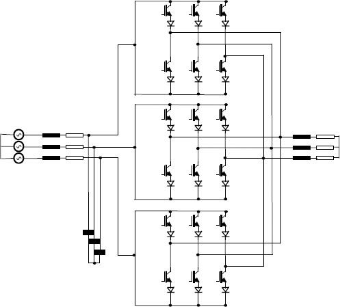
FIGURE 18.7 AC/AC matrix converter built of three 3-phase current source inverter modules.
Due to the symmetry of the power stage, there are two ways possible for the connection of the unidirectional switches. It is important to group the unidirectional switches as shown in Figure 18.7 with the DC side towards input. In this way, we avoid the need to short-circuit one converter leg when two output phases are connected to the same input. The generic SVM algorithm for matrix converters can be applied here. Figure 18.8 shows the actual implementation with IPM/IRAMS.
18.2.2 DYADIC MATRIX CONVERTER WITH VSI MODULES
Given some hardware limitations of the conventional matrix converter, novel topologies employing unidirectional switches have been proposed in [13,14,15,16] with very promising results. The scheme proposed in [17,18] consists of three power modules working as Unity Power Factor SPWM Rectifiers that are employed to form the three-phase output voltage system. These topologies are reviewed here with respect to their implementation with IPM modules. Each power module ensures near sinusoidal, unity power factor current on the input side, while a reduced value of the output capacitor allows us to control the converter output to track a sinusoidal waveform.
FIGURE 18.8 Realization of each CSI converter phase with conventional power modules.
The dyadic matrix converter theory was developed in [18] and it constitutes a possible base for the further development of PWM algorithms for any kind of direct AC-AC matrix converter. The output-input relationship is given by
(18.1) |
It has demonstrated that [H] can be decomposed into two matrices that are basically separating the frequency changer [Hf] and the static VAR compensator [Hφ] components:
(18.2) |
Moreover,
[Hf(t)]=[C12(0)C12(−2π3)C12(2π3)C12(−2π3)C12(2π3)C12(0)C12(2π3)C12(0)C12(−2π3)] |
(18.3) |
[Hφ(t)]=[C1φ(0)C1φ(0)C1φ(0)C1φ(−2π3)C1φ(−2π3)C1φ(−2π3)C1φ(2π3)C1φ(2π3)C1φ(2π3)] |
(18.4) |
Different forms for the above cell functions are considered in [19].
The schematic diagram of the matrix converter topology consisting of three 3-phase voltage-source converter modules is presented in Figure 18.9. Each converter module is controlled to produce, on its “DC-side,” an AC voltage superimposed on a DC voltage. The load does not see the DC components due to the 3-wire connection. The possibility to use three-phase voltage source converters packaged as power modules is the main advantage of this topology.
What concerns the control system, there are two possible ways of defining the control algorithm for a conventional matrix converter:
• Based on a scalar Sinusoidal PWM approach;
• Using a vector model of the AC/DC power converter.
While the original approach suggests the reference as being a sinusoidal waveform superimposed on a DC component (Figure 18.10a), a waveform with a higher content in third harmonic was proposed (Figure 18.10b). In this way, efficiency is improved as at any moment one converter does not work at all.
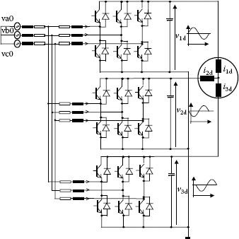
FIGURE 18.9 Schematic diagram of the power stage of the proposed three-phase voltage source matrix converter.
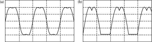
FIGURE 18.10 Load voltage: (a) sinusoidal reference; (b) novel reference.
The converters behave as current sources pumping current into capacitors used on the output side for the required voltage source character. For this reason, the actual waveforms of the output voltages are strongly influenced by the passive components of the system, including the output filter. This is true for both the sinusoidal reference and the waveform with a third-harmonic injection reference [19]. Closed loop PWM control improves further the system performance.
The major advantage of the control method proposed in Figure 18.10b consists in a larger available output voltage. Reversing the design requirement: the power converter works with 15.4% less voltage across the output capacitor bank (filter) for a desired maximum output (phase) voltage. Moreover, the maximum dv/dt across the capacitor is less by 50%. This permits a lower switching frequency of the converter for the same harmonic performance in the phase voltage. In some cases, the power switches can be chosen at a lower maximum direct voltage for the same desired output voltage.
Additional harmonic aspects are discussed in [19].
18.3 MULTILEVEL CONVERTER MADE UP OF MULTIPLE POWER MODULES
Multilevel converters are used for higher voltages in the DC bus and consist of a network of switches able to produce more voltage levels in the output (AC) voltage. Some examples for the use of IPM devices to the definition of novel topologies worth be mentioned here for the completeness of information. The scheme is shown in Figure 18.11.
A second approach for using IPM modules to building multilevel converters has been recently the subject of a PhD thesis at University of Bologna [21]. The base scheme is shown in Figure 18.12.
18.4 NEW TOPOLOGY BUILT OF POWER MODULES AND ITS APPLICATIONS
Given the inherent circuit loss and reliability issues with passive components, engineers have explored power conversion topologies able to alleviate the need for passive components. The resulted converters are often named direct converters. Among such alternatives, the cyclo-converters are a very old solution [22,23,24].
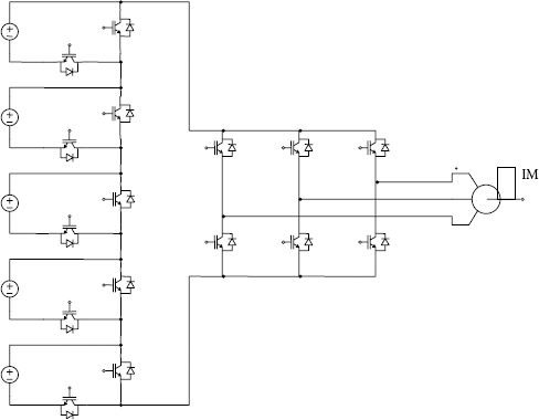
FIGURE 18.11 Novel multilevel topology built of Fuji IPM modules [20].
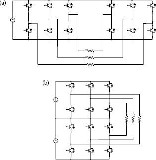
FIGURE 18.12 Series (a) and parallel (b) dual-IPM based multilevel converters (IRAMS).
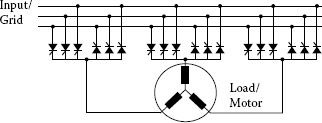
FIGURE 18.13 Principle of operation for a two-quadrant cyclo-converter.
Despite the advent of IGBTs, cyclo-converters are still used in high power applications, especially in applications such as cement mill drives, ship propulsion drives, rolling mill drives, Scherbius drives, grinding mills, mine winders, dynamometer equipment. The operation of a cyclo-converter is based on continuously changing the control angle of a SCR device in order to derive a waveform with a high content in fundamental at the desired load frequency. Figure 18.13 presents the operation principle for a three-phase to three-phase half-wave cyclo-converter. Each conventional rectifier can be controlled to vary its average output voltage between a positive maximum and a negative minimum, while the load current can have one direction only.
In order to achieve a full four-quadrant operation necessary for motor drives applications, two identical cyclo-converter systems of Figure 18.13 are connected in anti-parallel to form circulation paths for both negative and positive currents. Figure 18.14 shows the three-phase to three-phase full-wave cyclo-converter.
A modern and updated approach to the realization of direct conversion would build the four-quadrant cyclo-converter with IGBTs. Such converters can be seen as being similar to the matrix converters [25,26]. The topology is drawn in Figure 18.15 and the principle of operation is shown in Figure 18.16. The control method was changed from control of the firing angle to synchronized PWM algorithm, while the structure and operation of the system remains the same as for a cyclo-converter [27,28,29,30]. The advantage consists in achieving larger available voltages on the load with a simpler packaging strategy. These new converters are good competitors of the well-known multilevel converters, matrix converters, or power electronics systems series-connected through the open-winding loads.
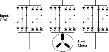
FIGURE 18.14 Full-wave four-quadrant cyclo-converters.
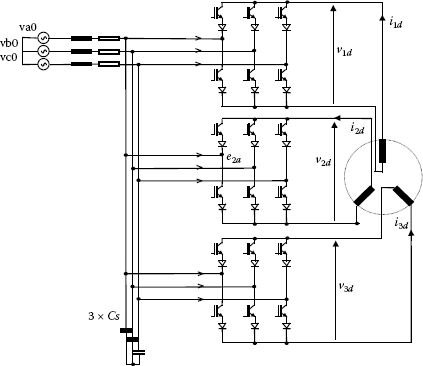
FIGURE 18.15 Implementation of the two-quadrant direct power converter.
The AC/AC direct converter previously described was first reported in 1976 [31,45[1]] with the devices and control specific to that time. Details of operation were reported in [15,16,17,18,19] along with a Space Vector Modulation controller derived from the knowledge about Current Source Converters. Parallel efforts defined the control based on matrix representation of the modulating waveforms [20,21].
Each phase current is derived by controlling the DC side of the conventional grid-interface CSI. Later on, we have proved that the grid-side currents can be controlled with unity power factor and low harmonic content, and this control can be extended even for unbalanced operation [27] or grid induced harmonics. The load-side current can be considered as a sinusoidal wave superimposed with a DC component. A special waveform (Figure 18.16b) has been considered in order to decrease the DC component to 82.8% and the current peak to 86.6% of the sinusoidal based solution.
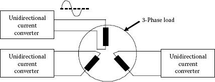
FIGURE 18.16 Two-quadrant IGBT-based cyclo-converter principle.
A possible performance comparison can be achieved with a current source converter used commonly for medium and high power drives. If the rotor winding is built with large bars or in the double-cage configuration in order to repress the current (for direct start at nominal frequency with lower starting current and larger torque), the dependency on frequency: Ks=0.4+0.97 ⋅ √f and can go up to 10. The proposed converter will dissipate less power inside the machine than the simple Current Source Inverter. Despite the harmonics reduction with PWM operation of the CSI, the machine loss is larger than that of the IGBT cyclo-converter and, more importantly, a large part of them are within the machine rotor.
The following waveforms explain the operation of the two-quadrant power converter, employing the control system described in the next section (Figure 18.17).
Figure 18.18 introduces the four quadrant direct AC/AC converter able to get closer to the industrial drives’ case. Using open-winding load is more realistic in high-power applications where the load is typically with both terminals of each phase available, but similar operations can be achieved with star-connected load. This power electronics system is composed of 6 conventional CSI converters operated with a variable DC-side current. The control of each individual CSI is described in the next section. It includes a compensation for unbalance or grid harmonics while the DC-side currents are controlled in closed loop.
Figure 18.19 shows the complete schematic of the power stage for the 4-quadrant converter built up of Current Source Inverter modules. Each module can be implemented independent of the system and its control requirements can easily be depicted from the system requirements. Designing and building individual current source converters is the only design task for this system.
Table 18.1 provides a comparison with the back-to-back multilevel converter and with the series-connected converters following a rectification with power factor correction. One can observe the ability to obtain sqrt(3) times more voltage than a matrix converter or other topology without any special over-modulation algorithm [32], and with less passive components.
Let us review the operation of each individual CSI converter. As shown in Chapter 16, there are many control algorithms previously reported in literature [33,34,35,36,37].
It is important to understand that the converter used in the application from Figure 18.20 behaves as a voltage source on the output side. At any moment, there are two switches turned-on and the converter output (conventional DC voltage of the AC/DC converter) equals the difference of the voltages across two input filter capacitors. The voltage pulses obtained as output voltages will be filtered by the machine inductance to produce the desired currents. Observing this provides an analogy between the outputs of the proposed converter and the outputs of a three-phase voltage source inverter. The control system uses a Space Vector Modulation based algorithm, and we are seeing the converter as a voltage source on the DC side. Hence, we can work with voltage vectors instead of the conventional current vectors (Figure 18.20).
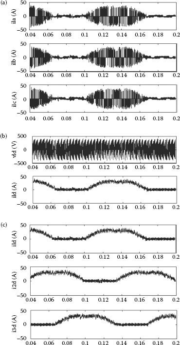
FIGURE 18.17 Waveforms for the first converter plus the command signals (fout = 10 Hz, Im = 30 A, fsw = 3.6 kHz, RL = 2 V, LL = 4 mH). (a) Input phase currents for one of the converters; (b) output phase current and output voltage for one converter; (c) output phase currents for all three converters. (From Neacsu, D.O. 1999. IEEE IECON 1999, San Jose, CA, USA, November 29–December 3. With permission.)
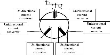
FIGURE 18.18 Four-quadrant direct AC/AC converter based on CSI modules.
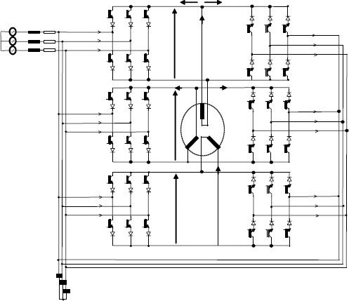
FIGURE 18.19 4-Q converter circuit diagram.
TABLE 18.1
Comparison Results for Four Quadrant IGBT Cyclo-converter
Hardware components (cost, size, weight) |
|||
4Q Cyclo-conv. |
Multilevel |
2-Series |
|
IGBT/diodes |
36 |
24 |
24 |
Input filter |
3× LC |
3× |
3× |
|
LCL |
LCL |
|
Waveform characteristics |
|||
4Q Cycloconv. |
Multilevel |
2-Series |
|
Max. output voltage (RMS) versus input Vph (RMS) |
0.866*sqrt(3)*Vph |
0.866*Vph |
2*Vph |
Peak of the output current at the same fundamental of phase current |
Sqrt(6)*Iph |
Sqrt(2)*Iph |
Sqrt(2)*Iph |
Operational and control characteristics |
|||
4Q Cyclo-conv. |
Multilevel |
2-Series |
|
Homopolar component in output current |
NO |
No |
No |
Smooth torque production |
YES |
Yes |
Yes |
Field-oriented vector control |
YES |
Yes |
Yes |
Input PF correction |
YES |
Yes |
Yes |
Figure 18.20 shows a low power diode rectifier for the sensing of the input grid voltage. The circuitry also contains an input filter, current control, and the PWM generator. Designing the PWM circuitry based on voltage vectors allows us to neglect the load character and more importantly to define closed loop current control with the output (actuating measure) as voltage reference. Finally, a PLL loop is used as frequency multiplier locked to the supply frequency in order to produce the desired sampling frequency. The influence of the supply frequency variations can be reduced further.
The theory of PWM control of a Current Source Converter is briefly revisited herein. More details are available in Chapter 15. The load current Id is considered as being constant during a PWM sampling interval, and it should be controlled to follow a variable reference over a fundamental frequency cycle.
Since one and only one switch in the upper and lower half bridge must be turned-on at a time, there are nine possible combinations for the “ON”-switches. Each pair of two switches turned-on determines a specific state of the converter and a Space Vector can be associated to each state. The output voltage can therefore coincide with any of the line-to-line voltages or can be zero. Only seven distinct positions of the Space Vector can be obtained: I1 − I6 and zero I0, and they are shown in Figure 18.21. The synthesis of any virtual position of the current vector in the complex plane can be achieved with different active states being combined over a sampling interval.
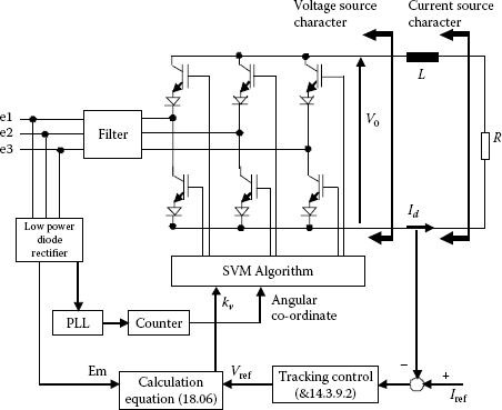
FIGURE 18.20 Grid interface with current source converter seen as voltage source on the DC side.
As shown in Chapter 16, any desired position of the space vector I is always placed between two space vectors Ia and Ib, (a,b = 1…6) which represent the two active states involved in the switching process. Writing the appropriate average relationship yields:
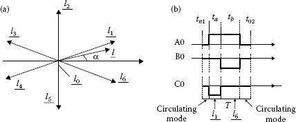
FIGURE 18.21 (a) Current space vector locations; (b) synthesis of a desired location of the space vector.
(18.5) |
where T is the sampling period; ta is the time assigned for the state Ia; tb is the time assigned for the state Ib; t0 is the time assigned for the state I0. The sampling interval is completed with a zero state that can be obtained by turning-on the switches on the same leg so that there is always a current path for the output inductive current.
Observing the circuitry from Figure 18.20 allows us to transform the current vector control into a voltage vector control. In this respect we need to consider the output voltage measured right after the power stage and before the load. This approach would further allow us to use the grid voltage as a feed-forward component able to compensate for harmonics or other grid distortion. Considering Em the envelope of the rectified input voltage [36, 37] and V the desired voltage vector at the output of the converter, the space vector theory can be re-written in voltage terms:
(18.6) |
where V is one of the desired references for the three-phases (v1d, v2d, v3d). The duration t0 is shared by two zero states.
Any unbalance of the grid voltage is reflected in the real-time envelope of the grid voltage Em, and hence it is compensated within the Space Vector Modulation algorithm (Figure 18.22). This compensation method benefits from the research results presented in [36]. This method has the drawback of limiting the maximum available voltage to the minimum value of Em. The design of the controller follows the description from Section 13.3.9.2 [38,39].
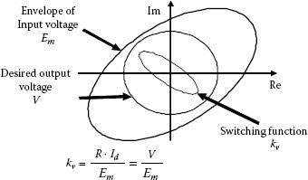
FIGURE 18.22 SVM for each power converter unit.
18.5 GENERALIZED VECTOR TRANSFORM
Some of the previous converters have used a special shape of the phase currents or voltages. This shape of the converter waveform has the interesting property that the difference from one phase to another is always a pure sinusoidal waveform. However, a link between vector control methods and the proposed waveforms is necessary. Conventional vector control methods have orthogonal (d, q) or (x, y) coordinates as outputs.
Let us consider a general set of three voltages [40]:
(18.7) |
that needs to be transformed in another set of voltages
(18.8) |
Usual vector control theory uses the time-invariant environment of d − q − 0 frame. We would like now to generalize this transform from a system with frequency ω1 to a system with frequency ω2 through an intermediary fixed gain DC controller. All possible control cases share the same general expression for the direct transfer function [Hf] [15],
(18.9) |
where
(18.10) |
represents a matrix composed of orthonormal base vectors of the input or output three-phase systems and [P] represents a matrix of constant weights pij. For a three-phase system, the vector space has a dimension of three and only three terms will always be seen in the matrix defined with base vectors.
Symmetries within a three phase system contribute to a generalized form of Equation 18.09:
[Hf(t)]=[C12(0)C12(−2π3)C12(2π3)C12(−2π3)C12(2π3)C12(0)C12(2π3)C12(0)C12(−2π3)] |
(18.11) |
A base within a vector space consists in a system of vectors B that provides a unique representation of any member V of that Vector Space as a linear combination of vectors from B. For our 3-dimensional vector space, it yields:
(18.12) |
or
(18.13) |
where vd, vq, v0 are also called coordinates. If the vector space has a finite dimension, then all possible bases have the same number of elements. A base is orthonormalized if all its vectors have unitary magnitude and any two different vectors are orthogonals.
Generally, analysis of three-phase power converters is considering the orthonormalized base vectors as
(18.14) |
(18.15) |
(18.16) |
When the zero-sequence is omitted, b3(ωi) does not appear in the frequency changer term.
The intermediary factor, Pf plays the same role as the turn ratio of the primary to secondary windings of a magnetic transformer. For example, we provide three possible cases herein:
A. Choosing
(18.17) |
yields
(18.18) |
B. Choosing
(18.19) |
yields
(18.20) |
C. A general dependency including both type of terms yields
(18.21) |
Due to the definition of a base in a vector space, a base is not unique and new vector bases can be defined. This demonstrates that selection of Equations 18.17, 18.18, 18.19 is not the unique choice for a three-phase system. It opens up a new mathematical tool for working with references not sinusoidal but characterizing uniquely a three-phase system. The resulting waveforms have been also used in discontinuous PWM algorithms.
Figure 18.23 presents two possible waveforms considered as examples for this approach. Furthermore, to simplify the mathematics, the third term corresponding to the homopolar component is neglected in this analysis.
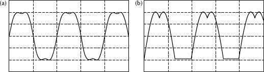
FIGURE 18.23 Different choices of output-side references functions.
Mathematical form of Figure 18.23a yields the following two functions that can be chosen as a base in a vector space.
[b1(ω2)]T=√23⋅[cosω2t+16⋅cos(3⋅ω2t)cos[ω2t−2π3]+16⋅cos(3⋅ω2t)cos[ω2t−4π3]+16⋅cos(3⋅ω2t)][b2(ω2)]T=√23.[sinω2t+16⋅sin(3ω2t)sin[ωit−2π3]+16⋅sin(3ω2t)sin[ωit−4π3]+16⋅sin(3⋅ω2t)] |
(18.22) |
Considering the same vector base from Equations 18.06 and 18.07 for C(ω1) and the new base functions (Equations 18.15 and 18.16) on C(ω2) yield the next form of the modulating signals.
[Hf]=[CD12(0,0)CD12(−2π3,0)CD12(−4π3,0)CD12(−2π3,−2π3)CD12(−4π3,−2π3)CD12(0,−2π3)CD12(−4π3,−4π3)CD12(0,−4π3)CD12(−2π3,−4π3)] |
(18.23) |
where
(18.24) |
Analogously, we can consider the base vectors
(18.25) |
(18.26) |
where f(ω2t) represents the waveform presented in Figure 18.23b and g(ω2t) represents the same waveform with 90° out of phase. It yields:
f(ω2t)=[u(ω2t)−u(ω2t−2π3)]⋅cosω2t+[u(ω2t−2π3)−u(ω2t−4π3)]⋅cos(ω2t−π3) |
(18.27) |
where u(x) represents the Heaviside function (= 0, for x < 0 and = 1 for x > 0).
Finally, denoting:
(18.28) |
yields
[Hf]=[CE12(0,0)CE12(0,−2π3)CE12(0,−4π3)CE12(−2π3,0)CE12(−2π3,−2π3)CE12(−2π3,−4π3)CE12(−4π3,0)CE12(−4π3,−2π3)CE12(−2π3,−4π3)] |
(18.29) |
18.6 IPM IN IGBT-BASED AC/AC DIRECT CONVERTERS BUILT OF CURRENT SOURCE INVERTER MODULES
The previous sections have laid down the theoretical background for several direct AC/AC power converters, with reduced count of passive components, that can be implemented with circuitry based on conventional Current Source Inverters (CSI). Unfortunately, there is no CSI inverter packaged unitary for this purpose. Attentive to the developments on the market of power semiconductor devices, voltage source inverters (intelligent power modules) can be used for building CSI converters. Figure 18.24 illustrates this hardware implementation.
The PWM algorithms previously defined for current source converters cannot work with the hardware from Figure 18.24 since they assume shorting the DC bus during the zero-states. Such operation is prevented by the internal operation of the intelligent power module and a short dead-time is generally introduced by such module to prevent shoot-through. Additional requirements for the bootstrap power supply should be met, that is frequently enough operation of the low-side switch.
A new PWM algorithm is needed to use opposite active vectors during the zero-states in order to avoid shoot-through. The two opposite vectors are used to compensate each other within the average vector equation used for Space Vector Modulation generation. The details of this PWM algorithm are explained with Figure 18.25.
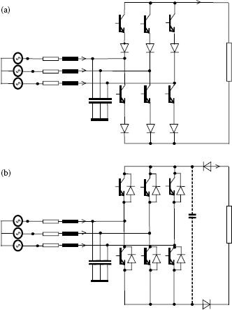
FIGURE 18.24 Conventional (a) and modified (b) CSI converters.
The vector applied during the first zero-state is selected to be the same as the nearby active vector, and the vector applied during the second zero-state is selected as the opposite of the vector applied during the first zero-state. Thus, the two vectors cancel each other over the average equation applied over the length of a sampling interval. Results for the current control over a single-phase are shown in Figure 18.26 for switching at 3 kHz. The overall number of switching processes remains the same. The same design of the current control and PWM generator is applied for all six power modules.
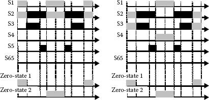
FIGURE 18.25 Conventional CSI algorithm (left) and VSI PWM algorithm (right).
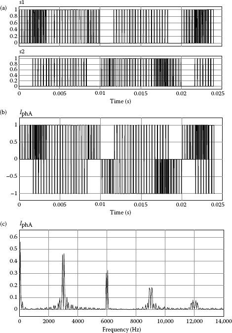
FIGURE 18.26 Converter operation with constant DC current at 3 kHz switching: (a) switching signals for top and bottom IGBTs, (b) phase current, (c) harmonic spectrum.
Figure 18.27 illustrates the implementation with Intelligent Power Modules (IPM). A small LC input filter may still be used on the grid side and it can be omitted if the grid is really stiff, satisfying the ideal voltage source requirement. On the grid side, each current is a summation of six currents, yielding a high content in fundamental.
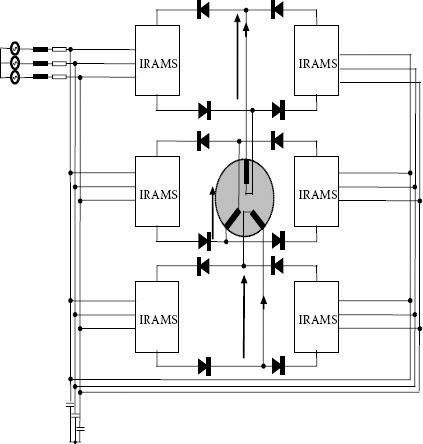
FIGURE 18.27 IPM/IRAMS implementation of the new converter.
The appliance market has recently seen a revolutionary change with the introduction of inverter-based motor drives. The appliance power system has the development structured into several levels:
• Conventional component level architecture
• Multiconverter subsystem level architecture
• Multiaxis and multiconverter system level architecture
The innovation of the appliance electronics is expected within the following subsystems:
• Semiconductors and packaging
• Circuit topology
• Communication and user interface
• Control algorithms
An important trend within the appliance power electronics relates to creation of integrated power modules based upon the merger of the device development with new circuit prototyping. The design criteria taken over from the system level design are Cost (product and maintenance), Energy Efficiency, Product lifetime and reliability, Influence on ambient medium (noise, temperature, grid harmonics, and so on).
The most important requirement for the appliance consumer market relates to system reliability. Different manufacturers show different customer expectations, with a high MTBF of 20 years lifetime with 90% reliability prevailing.
As discussed in Chapter 7, the electrolytic capacitor represents a critical component for the system lifetime since it has the lowest lifetime of all power conversion components. Capacitor lifetime is limited by the electrochemical degradation and accelerated by temperature and voltage stress. The lifetime of electrolytic capacitors has progressed from 1000 h at 65°C, 40 years ago, to up to 15,000 h at 105°C today. The lifetime is predicted by the capacitor vendors with the Arrhenius law equations. For instance, a capacitor rated with 10,000 at 105°C, could survive 160,000 at 65°C [39].
Hence, any solution that can eliminate passive components and/or reduce their importance in the calculation of the overall reliability is highly desirable. The AC/AC power converter subscribes to this concept, and the reliability is expected to be increased by the withdrawal of electrolytic capacitors.
It can be further proven that a power semiconductor module could contribute better performance to the system reliability than individual components. The IPM modules provide better thermal design and an excellent layout, both with effects on the system reliability. Using a power module supplied from the manufacturer rather than individual components is generally a better choice for the inverter application.
The previous sections have shown a series of novel direct AC/AC power converters derived from cyclo-converter concept, and intended to be implemented with standardized power modules. It is therefore attracting the use of this concept to the appliance market [39]. Since the most important advantage of using electronic control of motor drives consists of energy savings, the focus remains on cooling and thermal aspects of using this converter in the appliance application.
The thermal performance is presented herein in comparison with the conventional back-to-back solution. Thermal data is considered the same as in the manufacturer’s example for IPM utilization. The intelligent power module is IRAMS10UP60, with a junction-case thermal resistance of 4.7°C/W. The thermal compound was Wakefield #120 characterized by a thermal resistance of 0.1°C/W. The suggested heat-sink is an off-the-shelves component, Aavid Thermalloy #66365, with a heat sinking area of 0.63 × 1.50 in, and a thermal resistance of 5.4°C/W.
Section 2.4 has presented the loss calculation for the IGBT based medium power converters [41,42]. Given the peculiar construction of the IPM module, an empirical calculation of the loss is presented in [43] and adopted herein. The results of this method used for a conventional motor drive application show 2.3 W power loss per switch, and 14.1 W per entire package, when operated in ambient temperature and trying to prevent a junction temperature close to 125°C.
This empirical model considers each switch individually and calculates the power loss with the following set of equations already presented in Chapter 2.4 as Equations 2.22, 2.23, 2.24 valid for International Rectifier’s IRAMS devices.
(18.30) |
(18.31) |
(18.32) |
The number of switching processes during each switching period is necessary in order to use these equations for the loss calculation of the entire system (Figures 18.28 and 18.29).
A. Conventional back-to-back converter
Switching Loss—IGBT = Switching processes are shown in the next figure.
Conduction Loss—IGBT = 180° total.
Switching Loss—Diode = Diodes are switched during the negative half waveform (reference), with a partial conduction.
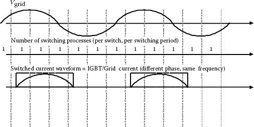
FIGURE 18.28 Distribution of switching processes used for switching loss calculation (conventional).
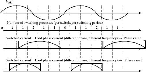
FIGURE 18.29 Distribution of switching processes used for switching loss calculation (IPM).
B. New topology based on multiple-IPM modules
Switching Loss—IGBT = Switching processes are shown in the next figure.
Conduction Loss—IGBT = 120° total.
Switching Loss—Diode = Diodes are moved outside of the IPM module, with same conduction, and no switching loss.
The number of switching processes is very similar with the back-to-back converter. In any direct AC/AC converter, the switching loss cannot be expressed very easily since the switched current depends on both the load and grid frequencies.
Reference [43] discusses a practical case: a 1HP = 745W A/C compressor operated from Vdc = 400 V, modulation index of 0.8, VLL = 113 Vrms, PF = 0.6, Iph = 6.35 Arms, fsw = 3 kHz. Table 18.2 shows comparison of results between the conventional back-to-back converter and the IPM-based cyclo-converter. The load current is assumed to be at the same frequency. The power dissipated per module reduces at least 56% and this reduction can be even more important for certain combinations of input and output waveforms.
It is worthwhile to reverse the design reasoning and to observe that the new topology can deal with a load of P = 2 kW (Iph = 9.25 Arms, motor PF = 0.6, nominal frequency and voltage conditions of 120 Vac/phase, 50 Hz, switching at 3 kHz), at the maximum thermal capacity of the setup. The system shown can therefore drive a 2 kW motor, in similar operation and thermal conditions as a back-to-back dual IPM module would drive a 1HP = 745 W motor.
The results are very impressive for the system power density and packaging: the entire power stage (with straight-pin mounting, six individual heat-sinks, passive LC filtering and power connectors) accounts for (2 × 2 × 7.5 in =) 0.49l for 2 kW delivered power (that is 4.1 kW/l) [39]. This should compare to current industry goals of 4 kW/l, for this class of converters [44].
TABLE 18.2
(a) Power Loss Distribution Per IPM Package, for 1HP Load, with Voltage and Current Dictated by Operation of the Back-to-Back Converter
Back-to-back converter |
New converter |
|
Psw, per switch |
0.32 W |
Up to 0.32 W |
Pcond, per switch |
1.49 W |
1.00 W |
Pdiode |
0.53 W |
0 |
Ploss, Entire IPM module |
14.1 W |
7.92 W |
(b) Power Loss Distribution Per IPM Package, for 2kW Load
New converter |
|
Psw, per switch |
0.75 W (variable) |
Pcond, per switch |
1.80 W |
Pdiode |
0 |
Ploss Entire IPM module |
15.30 W |
18.7 USING MATLAB-BASED MULTIMILLION FFT FOR ANALYSIS OF DIRECT AC/AC CONVERTERS
18.7.1 INTRODUCTION TO HARMONIC ANALYSIS OF DIRECT OR MATRIX CONVERTERS
The previous sections have presented several direct converter topologies [45], each with different control methods. It is well-known that the PWM operation of power converters produces harmonics at both input and output [46,47]. In the conventional bridge-like topologies, we have to deal with two frequencies: the modulating waveform’s fundamental frequency and the carrier/switching frequency. The challenges associated with the harmonic analysis of direct converters are multiple:
• The modulation signal contains both the input and output frequencies, typically independent from each other and without forming an integer ratio.
• The switching/carrier frequency is not a rational multiple of either the input frequency or the output frequency.
For a long time, the complex, vast, and time-consuming calculation required by the harmonic analysis of power switching converters encouraged the engineers to develop their own algorithms for a fast development in Fourier series [48,49,50,51,52]. The most used procedure consists of a double Fourier series expansion in two variables [48,52]. Later efforts presented the development for multiples frequencies [49,51]. Alternate results are given in [50,52]. All these solutions are providing a fast calculation of harmonics independent of the accuracy of the simulation model. However, they have a strong content in advanced mathematics and are each dedicated to a specific application. Hence, they are not very friendly for the practice engineers.
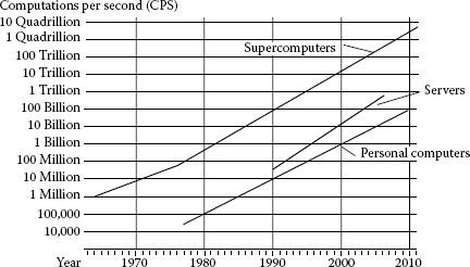
FIGURE 18.30 Evolution of processing power.
During this time, the Moore’s law acted upon the computing hardware and today we have computers based on dual-, or quad-core processors, with 64-bits bus, huge Terra-Bytes memory capacities, and high clock frequencies. Figure 18.30 [53] provides a quick update on the development of computers. It says that the same simulation model we ran in 1 h 10 years ago can be run in under 30s now.
Another illustration of the contemporary computing power makes 2012 the year when the power electronics simulation waveforms could be achieved in real-time for the first time. OPAL Corporation reported at Industry Forum of IECON2012 [54] the implementation of a complete motor-converter drive model on an advanced Altera FPGA with running at the system time scale. We consider this as one of the most important historic milestones for the simulations of power electronic systems.
These results should imply the advantages of using straightforward computer calculations for the analysis of power electronics waveforms. This is in par with technology development and it may diminish the academic struggle for harmonic calculation algorithms that unfortunately do not have too much practice value since the major manufacturers have settled already for their own algorithm.
The engineering practice of either multiconverter or multifrequency PWM converters provides signals not described with mathematical functions. Instead, these signals come from measurement acquired at a selected sampling interval from hardware or from simulation models (like in Matlab-Simulink, PSIM, Plexim, or alike), and hence they are not continuous but discrete signals. The duration of a signal is finite and in most cases it will not be the same as the period required by the Fourier Theorem or the signal may not be periodic at all. Due to these limitations, the frequency analysis devises a method to extract an estimate of frequency components which are not known a priori. The process is known as the Discrete Fourier Transform (DFT). Section 3.5 in Chapter 3 have introduced us to harmonic analysis of PWM converters. The following are reconsidering this information for revealing other computer related aspects necessary to analysis of direct (matrix) converters.
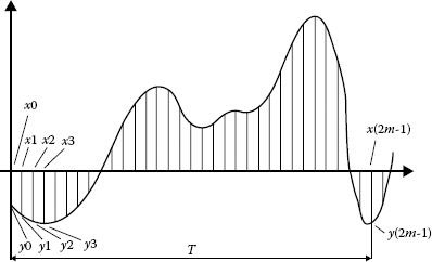
FIGURE 18.31 Sampling of the acquired time signal.
The Euler-Fourier integral can be calculated by approximation when the analyzed time interval is sampled at a fixed rate leading to 2 ⋅ m samples (Figure 18.31). Considering the Shannon Theorem confirms m different spectral lines.
It yields for each sample:
(18.33) |
This represents an approximation of the Fourier series and also a discrete calculation of the Fourier integral. When we know all the samples yq, each harmonic component can further be calculated with
(18.34) |
(18.35) |
(18.36) |
As shown in Section 3.5, the computer program yields very simple as structure:
• Calculate the argument β = π⋅q⋅n/m and the harmonic functions for each sample yq (q = 1,…, 2 m − 1);
• Calculate the individual products from An and Bn;
• Calculate An and Bn;
• Calculate the magnitude and phase for each harmonic.
For a reduced number of samples, performance can be improved when m is chosen as a multiple of 6 to speculate from the symmetries of the grid related waveforms. For an increased number of samples, the computer run time yields very large and some computer programs provide just calculation for the low frequency content. For instance, the instruction “FOUR” from SPICE provided a quick calculation for the first 9 harmonics only. SPICE after Version 5 allows us to specify the number of desired low frequency harmonics. The computer run time can also be reduced within the Fast Fourier Transform that represents a peculiar case of DFT.
DFT is a discrete equivalent for the Fourier Transform and the sampling of the latter may hide some properties. This means we need to be careful with the selection of the resolution for the DFT calculation. Usual source of errors in calculation of DFT comes from the smoothing effect given by the interpolation of results. This acts as a low-pass filter with attenuation of the harmonic magnitudes as frequency increases. For better results we need increased number of samples which are equivalent to a higher bandwidth low-pass filter.
Once the data is acquired from the experimental setup or from simulation, a postprocessing tool is employed for harmonic analysis. It is vital to understand very well the settings of the parameters involved in the FFT/DFT analysis.
A. Resolution
The more the number of points in the transform, the better the frequency resolution.
Other than speed, resolution is the only other difference between a 29 = 512-point transform and a 220 = 1,048,576-point transform. A power spectrum always ranges from the DC level (0 Hz) to one-half the sample rate being used. The number of points in the transform defines the power spectrum resolution (a 512-point Fourier transform would have 256 points in its power spectrum, while a 1,048,576-point fourier transform would have 524,288 points in its power spectrum).
For example, if we want to see separate 20 and 21 Hz frequency components in the power spectrum of a power converter waveform, a 512-point Fourier transform might not show these individual components clearly since its entire power spectrum is only divided into 256 equally spaced points and the desired frequencies are so close together. For samples acquired at 1 MHz (1 μs sampling), the frequency bins would be spaced at 1 MHz/512 = 1.94 kHz = 1940 Hz.
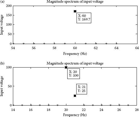
FIGURE 18.32 (a) A single 60 Hz grid voltage with 1Hz frequency step in FFT representation; (b) a good selection of parameters allows to clearly distinguish between 100 V/20 Hz and 25V/21 Hz components.
However, if the transform contains more points, it would be able to devote more points to the definition of closely spaced frequency components. In our example, a 1,048,576-point Fourier transform applied to a set of discrete signals depicted at a sampling rate of 1 μs, would space the frequency bins at 1 MHz/1,048,576 = 0.95 Hz. Re-arranging this selection yields Fs = 1,048,576 Hz = 1.048 MHz, and the frequency step 1 Hz. Thus, we are now able to see the difference between 20 and 21 Hz components (Figure 18.32b).
It is worthwhile here to make two comments:
• Most laboratory equipment sold as Spectral Analyzers offer a DFT with at most 32,768-points. In most cases they are not very suitable for analysis of power converters operated with both 50/60/400 Hz fundamental frequency and a carrier at 10−30 kHz. You can either benefit from the 0.1 Hz resolution through a windowing technique OR plot the entire range of DC-100 kHz with way lesser resolution.
• With the advent of computers, one can ask about the maximum number of DFT points we will ever need for analysis of power converters. Considering a maximum switching frequency of 50 kHz, a 1000-point PWM resolution (210 counter, 50 ns acquisition rate), and a 0.1 Hz resolution in frequency definition yields: 20 MHz/0.1 = 200,000,000–134,217,728 = 227.
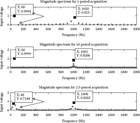
FIGURE 18.33 Spectral results when considering different time windows.
B. Accuracy
Figure 18.33 shows the spectrum of a signal composed of unity sine-wave components of 60 Hz and 1000 Hz, acquired over different time intervals. The spectrum appears somewhat spread out when we have a fractional number of periods (false harmonics in adjacent points) [51]. The spreading out (leakage) is due to energy being generated by the discontinuity at the end points of the waveform.
Solutions able to minimize this leakage effect consist of
• Use of conventional DFT instead of the optimized FFT;
• Multiplying the time series by a window weighting function before the FFT is performed.
Most window weighting functions attenuate the discontinuity by tapering the signal to zero at both ends of the window. With the window approach, the periodically incorrect signal will have a smooth transition at the end points which results in a more accurate power spectrum representation. However, if the waveform has important information appearing at the ends of the acquired time interval, it will be destroyed by this.
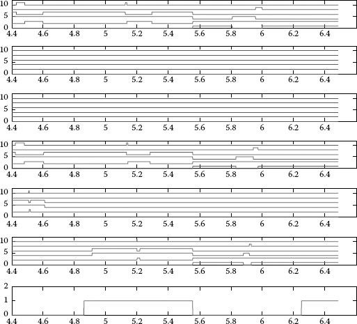
FIGURE 18.34 Example of PWM control signals for each of the six converters and the period flip-flop (twice the switching period).
Some popular windows are Hamming, Bartlett, Hanning, and Blackman. Each has different characteristics:
• The Hamming window offers the familiar bell-shaped weighting function, and produces a very good spectral peak with fair spectral leakage reduction only.
• The Bartlett window offers a triangular shaped weighting function and it produces a good, sharp spectral peak, good at reducing spectral leakage as well.
• The Hanning window offers a similar bell-shaped window and produces good spectral peak sharpness (as good as the Bartlett window), but the Hanning offers very good spectral leakage reduction (better than the Bartlett).
• The Blackman window offers a weighting function similar to the Hanning but narrower in shape. Because of the narrow shape, the Blackman window is the best at reducing spectral leakage, but the trade-off is only fair spectral peak sharpness.
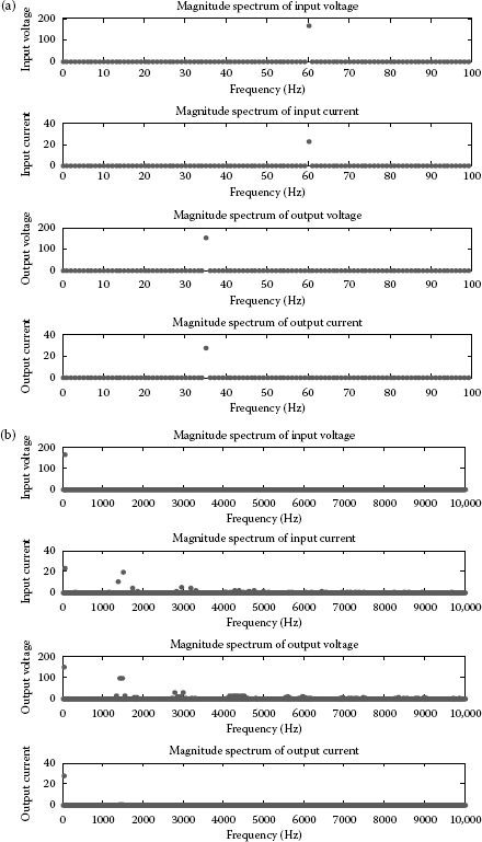
FIGURE 18.35 Sample of important waveforms for 1.44 kHz switching frequency on different zoom windows. (a) 100 Hz and (b) 10k Hz.
The choice of window function depends upon the trade-off between sharpness of peaks and decay of side-lobes. A Fourier analysis software package that offers a choice of several windows is desirable to eliminate spectral leakage distortion inherent with the FFT.
For the spectral-separation requirement of a direct power converter, the Blackman window is the best at bringing out the weaker term as a well defined peak.
MATLAB after Version 6.0 uses an implementation of the FFT called FFTW. The FFTW package was developed at MIT by Matteo Frigo and Steven G. Johnson (about 1997). Comparative studies performed on a variety of platforms show that its performance is typically superior to that of other publicly available FFT software, and it is even competitive with vendor-tuned codes (like in some hardware Spectral Analyzers). Contrary to vendor-tuned implementation, its performance is portable: the same program will perform well on most computer architectures without modification. Hence the name “FFTW” stands for the self-proclaimed title of “Fastest Fourier Transform in the West.”
No tuning or window selection is required in MATLAB when the dimension of the DFT is a power of 2. Moreover, for DFT dimensions that are powers of 2 between 214 and 222, special preloaded information from MATLAB’s internal database is used to optimize the computation.
The execution time for 1,048,576 real samples is less than a fraction of a second for a modern laptop [55].
18.7.4 ANALYSIS OF A DIRECT CONVERTER
A. Operation
We will use the above choice of a MATLAB DFT algorithm to the case of a direct converter. The operation of this multiconverter structure was explained in previous papers [15,16,17,18,19], and it follows the control of six Current Source Converters interconnected to provide a voltage source character on the load directly from the line-to-line grid voltages (Figure 18.34). The Space Vector Modulation is implemented herein with the sequence:
Zero-state → active 1 → active 2 → active 2 → active 1 → zero-state
that is very advantageous in terms of minimizing the number of switching processes. The two zero-states within a sampling interval are equal with each other. A sample of the result is shown. We can see that three converters work at a given moment only. Moreover, pulses are distributed with the same sampling period.
A complete harmonic analysis is performed for a switching frequency of 1.44 kHz, for a converter with a highly inductive load, when a 35 Hz output waveform is created with a lower voltage magnitude (Figure 18.35).
B. Feed-Forward Compensation of the Grid Voltage
The operation of each converter produces a modulation of the output voltage with the envelope of the three-phase grid voltage. The time·voltage product corresponding to each pulse will thus depend on the instantaneous grid voltage. This yields a time-varying spread-spectrum of the output voltage and input current.
A compensation of the PWM generator based on the actual value of the grid voltage helps in providing the load with the desired time·voltage product for each PWM pulse. This has advantages in both stability of any closed–loop system and compensation of grid unbalances. Harmonic results for compensation of an 85% unbalance are shown for the first phase voltage (Figure 18.36). Differences can be seen in the spectra of the output voltages at under 400 Hz.
For a balanced grid, there should be no difference in between the spectra of the output voltage with or without compensation (also called adaptive PWM [25]) if the DFT parameters are selected properly. This is because there should be enough cycles of fundamental frequency to average the varying effect of the grid voltage envelope when the resolution is set to 1 Hz or under. This remark can also be used backwards, as a tool to detect proper use of the FFT/DFT analysis.
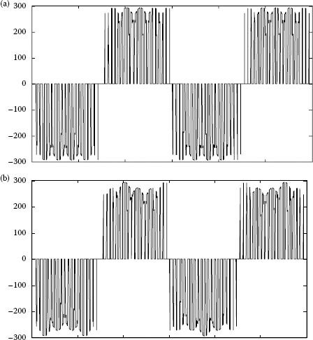
FIGURE 18.36 (a) Output voltage for the balanced input grid voltage; (b) Output voltage for 85% unbalance in the first phase of the grid voltage; (c) Spectra for PWM without compensation; (d) Compensation with input voltage measurement.
Stochastic ripple cancelation for interleaving the PWM controllers.
C. Synchronized PWM
The study of Space Vector Modulation algorithms has outlined the advantages of using an integer ratio between the sampling/switching frequency and fundamental frequency equal to a multiple of 6. This will benefit from all the symmetries in the complex plane representation and would avoid fluctuation of the cycle-by-cycle RMS (a cycle being defined at fundamental frequency).
However, spectral analysis with a fractional ratio between switching and fundamental frequencies shows that differences are minimal when the acquisition time is long enough (around 50 cycles). No important leakage is seen.
D. Using Interleaved Carriers
Interleaved operation of power converters is well-known for conventional bridge-type converters. Each dual (or bidirectional) converter corresponding to an output phase is controlled with a SVM carrier at 120° from each other. Contrary to interleaving conventional bridge-like converters, the instantaneous references for the three converters are different. Hence, the input current presents a stochastic ripple reduction of minimum √ N = √ 3 = 1.73 only [56]. All other waveforms and harmonics stay the same as in the case without interleaving (Figures 18.37 and 18.38).
18.7.5 AUTOMATION OF MULTIPOINT THD AND HCF ANALYSIS
Figures 18.39, 18.40, 41 show results for a back-to-back converter with a stepped-up 420 V DC bus, and open-neutral. Obviously, the number of actual switching processes differs from the direct converter despite the same PWM frequency of 1.44 kHz.
FIGURE 18.37 Stochastic ripple cancellation for interleaving the PWM controllers.
FIGURE 18.38 PWM control signals for each of the six converters, under interleaved operation (compare to Figure 18.34).
FIGURE 18.39 THD for output voltage at different output magnitude and frequency.
FIGURE 18.40 HCF for output voltage at different output magnitude and frequency.
FIGURE 18.41 THD of the input current at different output magnitude and frequency.
18.7.6 COMMENTS ON COMPUTER PERFORMANCE
Table 18.3 suggests running times for two conventional Windows-based computer architectures. The processing speed can be increased further by running the MATLAB code on the laptop’s more powerful Graphics Processing Unit card (GPUs like NVidiaGT555M with 144 CUDA cores) through the MATLAB’s Parallel Computing Toolbox. Users suggest a four times speed-up compared to the quad-core CPU.
TABLE 18.3
Computer Processing Power
Computer |
Simulation |
4-ch DFT |
THD/HCF graph |
Pentium 4, CPU 3.2 GHz, 1G RAM |
10,000 s |
~4 s |
~120 s |
Quad-Core i7, CPU 3.4 GHz, 8G RAM |
~2900 s |
~1 s |
~40 s |
1. Neacsu, D.O. 2012. Principle of a novel component minimized active power filter for high-power magnet supplies. IEEE Industrial Electronics Conference IECON, Montreal, Canada, October.
2. Neacsu, D.O. 2010. Analytical investigation of a novel solution to AC waveform tracking control. IEEE International Symposium in Industrial Electronics, Bari, Italy, July, pp. 2684–2689.
3. Huber, L., Borojevic, D., and Burany, N. 1992. Analysis, design and implementation of the space vector modulator for forced-commutated cycloconverters. IEE Proceedings of the Series B, 139(2), March, pp.103–113.
4. Neacsu, D.O. 1995. Theory and design of a space vector modulator for AC–AC matrix converter. European Trans. Electrical Power Eng. 4, 285–292.
5. Nielsen, P., Blaabjerg, F., and Pedersen, J.K. 1996. SVM matrix converter with minimized number of switchings and a feedforward compensation of input voltage unbalance. PEDES ’96, New Delhi, India, 8–11.
6. Holmes D.G. 1992. The general relationship between regular-sampled pulse width modulation and space vector modulation for hard switched converters. IEEE-IAS Annual Meeting, pp. 1002–1009.
7. Zhou, K. and Wang, D. 2002. Relationship between space-vector modulation and three-phase carrier-based PWM: A comprehensive analysis [three-phase inverters]. IEEE Trans. IE 49(1), 186.
8. Casadei, D., Serra, G., and Tani, A. 1996. A general approach for the analysis of the input power quality in matrix converters. IEEE PESC ’96, Baveno, Italy, vol. 2, pp. 1128–1134.
9. Nielsen, P., Casadei, D., Serra, G., and Tani A. 1996. Evaluation of the input current quality by three different modulation strategies for SVM controlled matrix converters with input voltage unbalance. PEDES ’96, New Delhi, India, January 8–11.
10. Neft, C.L. and Shauder, C.D. 1988. Theory and design of a 30-HP matrix converter. Proceedings of IEEE IAS ’88, pp. 248–253.
11. Halasz, S., Schmidt, I., and Molnar, T. 1995. Matrix converters for induction motor drive. EPE’95, Sevilla, Spain.
12. Watthanasarn, C., Zhang, L., and Liang, D.T.W. 1996. Analysis and DSP-based implementation of modulation algorithms for AC/AC matrix converters. IEEE-PESC1996 Conference Record, vol. 2, pp. 1053–1058.
13. Ziogas, P.D. 1986. Rectifier-inverter frequency changers with suppressed DC link component. Trans. Ind. Appl. IA-22(6), 1027–1036.
14. Kazerani, M. and Ooi, B.T. 1993. Direct AC-AC matrix converter based on three-phase voltage source converter modules. Proceedings of IECON 1993, Mavi Lahaina, Hawaii, November 15–19.
15. Ooi, B.T. and Kazerani, M. 1994. Application of dyadic matrix converter theory in conceptual design of dual field vector and displacement factor controls. IAS Annual Meeting, pp. 903–910.
16. Kim, S., Sul, S.K., and Lipo, T.A. 1998. AC to AC power conversion based on matrix converter topology with unidirectional swtches. APEC, Anaheim, CA, pp. 301–307.
17. Kazerani, M. and Ooi, B.T. 1993. Direct AC-AC matrix converter based on three-phase voltage source converter modules. Proceedings of IECON, Mavi Lahaina, Hawaii, November 15–19.
18. Ooi, B.T. and Kazerani, M. 1994. Application of dyadic matrix converter theory in conceptual design of dual field vector and displacement factor controls. IAS Annual Meeting, pp. 903–910.
19. Neacsu, D.O., Alistar, A., and Kazerani, M. 2002. Insightful analysis of carrier PWM algorithms for direct AC-AC matrix converters based on voltage-source converter module. IEEE IAS 2002, Pittsburg, USA, October 13–19, vol. 1, pp. 459–465.
20. Su, G.J., Adams, D., and Multilevel, D.C. 2001. Link inverter for brushless permanent magnet motors with very low inductance. IEEE IAS Annual Meeting.
21. Lega, A. 2009. Multilevel converters: Dual two-level inverter scheme. PhD Dissertation, University of Bologna.
22. Mohan, N., Undeland, T., and Robbins, W. 2002. Power Electronics. 3rd edition. John Wiley and Sons, New York.
23. Trzynadlowski, A. 2010. Introduction to Power Electronics. John Wiley and Sons, New York.
24. Trzynadlowski, A. 2010. Introduction to Power Electronics. John Wiley and Sons, New York.
25. Huber, L. and Borojevic, D. 1991. Space vector modulation with unity power factor for forced commutated cycloconverters. IEEE IAS’91 Conference Record, vol. I, pp. 1032–1041.
26. Chu, R.F. and Burns, J.J. 1989. Impact of cycloconverter harmonics. IEEE Trans. Industry Appl. 25(3), 427–435.
27. Neacsu, D.O. 1999. Current-controlled AC/AC voltage source matrix converter for open-winding induction machine drives. IECON, Denver, USA.
28. Kazerani, M. 2001. A direct AC/AC converter based on current-source converter modules. IEEE PESC, Vancouver, Canada.
29. Neacsu, D.O. 2003. IGBT-based “cycloconverters” built of conventional current source inverter modules. IEEE International Symposium SCS 2003, Iasi, Romania, July 10–11, vol.1, pp. 217–220.
30. Neacsu, D.O. 2004. Analysis and design of IGBT-based AC/AC direct converters built of conventional current source inverter module. IEEE IAS, Seattle, WA, October 2004, vol. 3, pp. 1824–1831.
31. Jones, J. and Bose, B.K. 1976. A frequency step-up cycloconverter using power transistors in inverse series mode. Int. J. Electron. 41(6), 573–587.
32. Neacsu, D.O., Rajashekara, K., and Gunawan, F. 2006. Overmodulation algorithm for zero-switching modulation. IEEE ISIE 2006, Montreal, Canada, July 9–12, pp. 1299–1304.
33. Weinhold, M. 1991. Appropriate pulse width modulation for a three-phase PWM AC to DC converter. EPE J. 1(2), 139–148.
34. Ciscato, D. 1992. PWM rectifier with low DC voltage ripple for magnet supply. IEEE Trans. IA. 28(2), 414–420.
35. Pan, C.-T. and Chen, T.-C. 1993. Modeling and analysis of a three phase PWM AC-DC converter without current sensor. IEE Proc. B 140(3), 201–208.
36. Enjeti, P. and Xie, B. 1992. A new real time space vector pwm strategy for high performance converters. IEEE/IAS Annual Meeting Conference Record, pp. 1018–1025.
37. Neacsu, D.O., Pastravanu, A., and Lucanu, M. 1993. Space vector based PWM AC/DC converter. IEEE CAS Section SCS93 International Symposium, Iasi, Romania, November 4–5, pp. 252–255.
38. Neacsu, D.O. 2010. Analytical investigation of a novel solution to AC waveform tracking control. IEEE International Symposium in Industrial Electronics, Bari, Italy, July, pp. 2684–2689.
39. Neacsu, D.O. 2010. Towards an all-semiconductor power converter solution for the appliance market. IEEE Industrial Electronics Conference IECON, Glendale, AZ, USA, November.
40. Pan, C.T. and Chen, T.C. 1993. Modeling and analysis of a three phase PWM AC–DC converter without current sensor. IEE Proc. B 140(3), 201–208.
41. Blaabjerg, F. and Pedersen, K. 1997. Optimized design of a complete three-phase PWM-VS inverter. IEEE Trans. Power Electron. 12(3), 567–577.
42. Neacsu, D.O. and Takahashi, T. 2000. Computer-aided design of a low-cost low-power snubberless three-phase inverter. IEEE Workshop on Computers in Power Electronics, Blacksburg, VA, June, pp. 204–210.
43. Wood, P., Battello, M., Keskar, N., and Guerra, A. 2002. IPM application overview—Integrated power module for appliance motor drives. International Rectifier AN-1044.
44. Staunton, R.H., Ozpineci, B., Theiss, T.J., and Tolbert, L.M. 2003. Review of the state-of-the-art in power electronics suitable for 10 kW military power systems. ORNL/TM-2003/209 Annual Report, October.
45. Friedli, T. and Kolar, J.W. 2012. Milestones in matrix converters. IEEJ J. Industry Appl. 1(1), 2–14.
46. Holmes, G. and Lipo, T.A. 2003. Pulse Width Modulation for Power Converters: Principles and Practice. John Wiley and Sons, New York.
47. da Silva, E.R.C., dos Santos, E.C., and Jacobina, C.B. 2011. Pulsewidth modulation strategies. IEEE Industrial Electron. Magazine 5(2), 37–45.
48. Bowes, S.R. and Bird, B.M. 1975. Novel approach to the analysis and synthesis of modulation processes in power converters. Proc. Inst. Electr. Eng. 122, 507–513.
49. Odavic, M., Sumner, M., Zanchetta, P., and Clare, J.C. 2010. A theoretical analysis of the harmonic content of PWM waveforms for multiple-frequency modulators. IEEE Trans. Power Electron. 25(1), 131–141.
50. Fedele, G. and Frascino, D. 2010. Spectral analysis of a class of DC–AC PWM inverters by Kapteyn series. IEEE Trans. Power Electron. 5(4), 839–849.
51. Wang, B. and Sherif, E. 2013. Spectral analysis of matrix converters based on 3-D Fourier integral. IEEE Trans. Power Electron. 28(1), 19–25.
52. Gabriel, G.J. 2000. A general analytical theory of frequency conversion. IEEE Trans. Circuits Syst. I Fundamental Theory Appl. 47(2), 189–199.
53. Anon. 2012. The rise of the machines. Popular Science (www.popsci.com/content/computing).
54. Lapointe, V. 2012. Using FPGA-based simulator to design and test power electronic controls used in automotive, industrial systems, aircrafts, micro-grid and MMC HVDC. IEEE IECON Ind. Forum, Montreal, Canada.
55. Anon. MATLAB DFT, Internet R2012b Documentation.
56. Perreault, D.J. and Kassakian, J. 1997. Analysis and control of a cellular converter system with stochastic ripple cancellation and minimal magnetics. IEEE Trans. Power Electron. 12(1), 145–152.