
AC/DC Grid Interface Based on the Three-Phase Voltage Source Converter |
13.1 PARTICULARITIES—CONTROL OBJECTIVES—ACTIVE POWER CONTROL
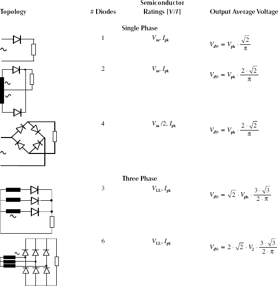
As energy is mostly transported on AC lines, electronic circuits able to convert AC to DC voltages have been the first application ever for power semiconductor devices [1,2,3,4,5,6]. The diode rectifier is the simplest power converter grid interface (Figure 13.1). At larger power levels, energy is transported and distributed within three-phase systems, and conversion from three-phase AC to DC voltage is used. All design aspects of diode rectifiers are thoroughly presented in university textbooks for power electronics and will not be reproduced here. However, Table 13.1 reviews the possible diode rectifier solutions and the appropriate factors for the waveform quality.
It is important to note that the high harmonic content of the grid currents may not be in accordance with the modern standards for power quality for certain power levels. Chapter 1 has shown some of the main requirements expected from power converters in different countries. It is easy to observe that above a certain level of the grid current, this class of topologies does not satisfy power quality requirements.
The second obvious disadvantage of this topology is the lack of control for the output voltage. Historically, this drawback was first tackled with thyristor (SCRs)-based converters (Figure 13.2). Their operation assumes a phase control and an output voltage lower than the diode rectifier’s output voltage. The waveforms corresponding to the operation of this power stage outline the low power factor and large reactive power circulated in the system.
The advent of power semiconductor devices with turn-off capability has improved the power quality factors for the grid currents. The first use of gate turn-off thyristor (GTO) devices within the diode or SCR-rectifier topologies has opened a new class of power converters. Examples of pioneering solutions are shown in Figure 13.3.
The output voltage results in a train of pulses characterized by a DC component and an HF-switching component. The grid current equals the algebraic sum of the currents through two devices and follows the pulse control strategy. This allows total harmonic distortion (THD) or, generally, the harmonic content of the grid current to improve. Given the large inductance in the load, a pulse is seen in the line current during each interval when a voltage pulse is generated on the load (Figure 13.4).
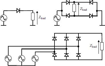
FIGURE 13.1 Different topologies of diode rectifiers.
If the number of pulses is small, a control strategy able to eliminate low harmonics (5th, 7th, 11th, 13th, and so on) of the current waveform is employed. Details of designing a pulse width modulation (PWM) controller suitable for such an operation are presented in Chapter 4. If the power semiconductor devices allow a higher switching frequency, a sinusoidal PWM algorithm may be considered. Two switches are controlled at a given moment and the pulse width is derived with a sinusoidal law.
All these circuits switch current through the grid lines. They introduce a line inductance in the path of the switch current, creating overvoltage at switching. To overcome this, snubber capacitors are needed across the power semiconductor devices (Chapters 2 and 3).
All the previously introduced power converters ensure energy conversion towards a load with a large inductance. This is the case when a DC machine drive or a DC magnet supply is used. However, a large group of applications require supply of the load with a constant DC voltage. This includes also the case of a grid interface for AC machine drives in which the DC circuit is dominated by a very large capacitor. Details about rating the DC bus and the importance of the proper value for a specific AC machine drive application are discussed in Chapter 4. We present here the details of the grid interface.
The simplest circuit able to create voltage on the DC intermediary circuit is based on a diode rectifier. As both the grid and the DC bus are voltage sources, an inductance should be used to take over instantaneously the differences between these two voltage sources. Different solutions use the inductance on the DC side, on the grid side, or on both sides. When the inductance is on the DC side, the circuit operation is identical to the previous diode rectifier with a large inductive load. The rectifier bridge produces an output voltage following the envelope of the grid voltages, and the inductance acts as a filter to produce the constant DC bus voltage (Figure 13.5).
When the inductance is on the AC side, the diodes have a shorter conduction angle depending on the actual voltage of the DC bus capacitor. Figure 13.6 shows the topology and the main waveforms for this AC/DC converter. When the difference between two line voltages is larger than the DC bus voltage, a pair of diodes turns on and the capacitor voltage follows the grid line-to-line voltage (VLL).
TABLE 13.1
Performance of Different Diode Rectification Schemes without Output Capacitor Filter
This interval corresponds to charging energy within the DC bus capacitor. When the DC bus voltage reaches the level of VLL, the diodes turn-off and the load is supplied solely from the capacitor bus. During the short conduction time interval of the diodes, the charging current is quite high, as it is produced across a small grid inductance from a large voltage difference. Moreover, the charging current at the start-up is very high until the bus voltage reaches the envelope of the grid voltages.
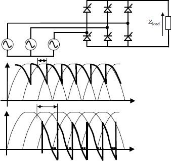
FIGURE 13.2 SCR based bridge converter and output voltage waveforms for different phase angle control.
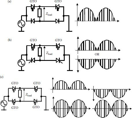
FIGURE 13.3 Use of GTO devices within the single-phase grid interfaces.
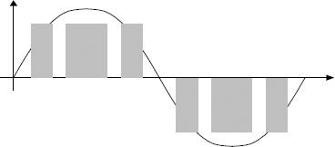
FIGURE 13.4 Pulses within the grid current.
The output of the rectifier bridge represents a quasi-constant DC voltage with a level dictated by the grid peak voltage. The level of the DC bus voltage depends slightly on the load. If there is no load, the DC voltage follows exactly the peak of VLL. The higher the load current, the larger the ripple of the voltage across the capacitor produced by subsequent charge–discharge events. The maximum ripple corresponds to the diode rectification waveform of VLL.
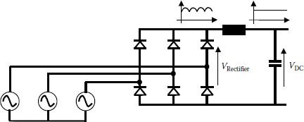
FIGURE 13.5 Diode rectifier with an inductive filter on the DC side.
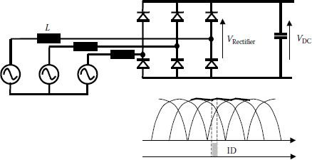
FIGURE 13.6 Diode rectifier with an inductive filter on the DC side.
13.2 MEANING OF PWM IN THE CONTROL SYSTEM
13.2.1 SINGLE-SWITCH APPLICATIONS
As previously shown, there is no control of the level of the DC bus voltage, and the grid currents are formed of pulses of current. A simple solution would consist of a buck or boost converter following up the DC capacitor (Figure 13.7).
There is a double DC stage within these converter topologies and this implies large filter DC capacitors. A closer analysis shows that the output voltage can be achieved after a multiplication of the switching functions corresponding to the two power-converter stages. This is equivalent to considering a single-capacitor filter at the output of the second power converter. In other words, it is possible to use the rectified voltage directly at the input of the buck or boost converter.
Moreover, it is desirable that the grid current be as close as possible to a sinusoidal waveform with reduced harmonics. The operation of the boost converter ensures this behavior of a continuous input current, with a waveform close to a given reference. This is because the inductor appears on the grid side and the inductor current is not chopped during operation. The resulting possible topologies are shown in Figure 13.8. Among these, the circuit with grid-side inductance is preferred because of the AC character of the current through inductors. The second major advantage of this topology consists of the inherent high power factor of the grid current.
Rectifying the AC input using a diode rectifier and chopping it at a high frequency to achieve voltage control has the advantages of simplicity, performance, and reliability. A diode rectifier cascaded with a PWM boost chopper is analyzed in [7,8,9,10,11,12,13]. In the first solution [7], the boost inductance is present in the grid side as phase inductance (Figure 13.8a). The analysis and design of this converter is further described in the work of Kolar et al. [8,9].
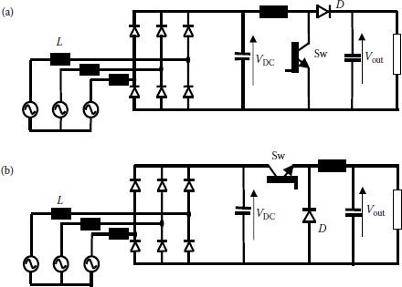
FIGURE 13.7 DC/DC converters following up a diode rectifier stage.
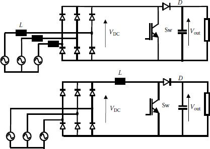
FIGURE 13.8 Three-phase single-switch boost converter.
The step-up (boost) converter operates at constant frequency in the discontinuous mode. This mode presents some disadvantages:
• Higher voltage/current stress
• EMI propagation
Advantages consist of
• High input power factor
• Reduced power loss through zero-current switching
• The absence of reverse recovery problem in the diodes
• The possibility of single control loop to control output power and voltage
Using this approach in high-power applications operated with low switching frequency and producing a low output voltage leads to a lower grid power factor and a current THD greater than 5%. One solution consists of injecting a harmonic content within the control of the switch in order to compensate for the main current harmonics.
The conventional control of the boost converter grid interface is simple, but the advantages of PWM are not fully utilized yet. It has been shown in the work of Weng and Yuvarajan [12,13] by extensive computer analysis that the input current distortion for a single-phase converter is reduced when employing a PWM with a second harmonic signal injected within the reference. The reference signal for the PWM generation is usually a DC value able to define the output voltage level. By injecting a second-order harmonic synchronized with the grid, the inherent variations of the output voltage and input current with the phase of the grid are reduced (Figure 13.9).
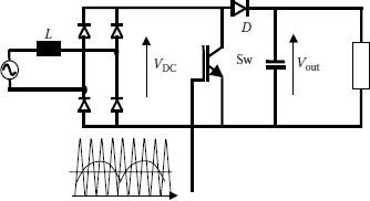
FIGURE 13.9 Injection of the second harmonic within the reference signal of a single-phase boost converter.
The circuit contains a low-pass grid filter that allows the input voltage to be seen directly at the converter input. The second inductance of the filter (Lb) also acts as a boost inductance for the converter. The switch used in this boost converter can be power MOSFET or insulated gate bipolar transistor (IGBT), depending on the application.
When the IGBT “Sw” is ON, the boost inductances are supplied by phase voltages and energy is stored in their magnetic fields. Depending on the phase of the input voltages, three diodes are in conduction at any time. This ON-time interval usually has a constant width and it can modify the output voltage on the basis of the duty ratio. When IGBT is turned-off, the energy stored within the boost inductance is transferred to the output capacitor. As with any boost converter in discontinuous conduction mode, the transfer to the output capacitor is ended when the current vanishes. The duration of this operation (toff1) until the first phase current reaches zero depends on the stored energy and, therefore, on the value of the lowest phase voltage. Observing the phase voltages within a three-phase system defines 12 intervals for analysis, each interval having a different phase voltage with the lowest value. The following discharge interval (toff2) is characterized by the conduction of two diodes only.
Figure 13.10 shows PSPICE simulation results, for example, for the current waveforms given for the case vR > 0, vs < 0, vT < 0. The first current to reach zero is on phase T. Maximum values of the current are denoted by Im,r(s,t) and current levels in the first two phases when the third-phase current vanishes are denoted by I0,r(s). The second waveform always represents voltage shape at the diode rectifier input on the corresponding phase.
From this generic operation of the power stage, different PWM control solutions are considered in the work of Kolar et al. [9].
• Constant ON time and constant switching frequency.
• Variable switching frequency depending on IGBT’s turn-on immediately after the end of the inductance’s discharge interval, with operation at the border of discontinuous conduction mode.
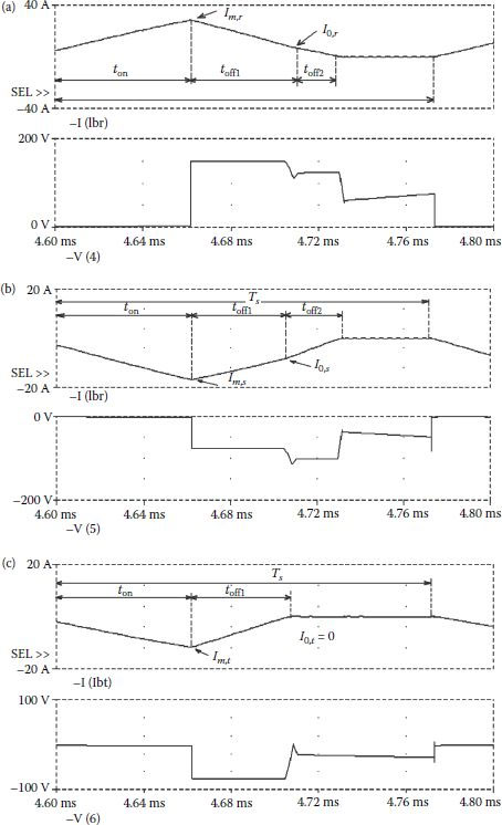
FIGURE 13.10 Shapes of the converter input currents and voltages (a) Phase R, (b) Phase S, (c) Phase T. (From Neacsu, D.O., Yao, Z., and Rajagopalan, V. 1986. IEEE PESC Conference, June 1996, Baveno, Italy, 24–27, pp. 727–732, IEEE Paper 0-7803-3500-7/96. © (1986) Printed with permission from IEEE.)
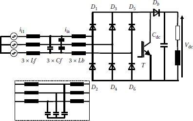
FIGURE 13.11 Basic Single-Switch Three-Phase Boost Converter.
• Maintaining a constant DC power flow on the DC side by a highly dynamic output voltage control. This solution requires a very large bandwidth of the system.
Understanding all aspects of the operation of the power converter shown in Figure 13.11 and the principles of the harmonic injection, as explained in Figure 13.9, for the single-phase converter allows the development of a special PWM algorithm with performance improvements. The duration of the first time interval after the IGBT’s turn-off depends on the instantaneous value of the lowest phase voltage, and this can be compensated for by an appropriate modulation of the reference signal for the PWM control. If the constant duty cycle of the conventional operation is denoted by D0, the new reference signal for the PWM control is given by:
(13.1) |
The injected harmonics are included in the f(t) function. The ON time of the switch is defined as:
(13.2) |
A qualitative analysis of the converter operation reveals the important six order harmonic as a component of the f(t) function. There are different methods to define the exact or mathematical form of this function. Many solutions are mainly based on repetitive simulation or experimental analysis. In what follows, an analytic solution for a problem of optimality imposed to the theoretically derived expressions of phase currents is provided and implemented based on a computer program.
However, this optimal PWM improves the harmonic performance at the input of the power converter stage and the actual filter also influences the grid harmonic performance.
Let us derive the mathematical expressions for currents through the boost inductance [13] assuming:
• Symmetrical three-phase system with no neutral components.
• Neglect of losses in the converter.
• Same value of the boost inductors in all three phases.
• All currents are positive when entering the power stage and negative when they flow into the grid.
• High switching frequency allowing an approximation of constant grid voltages over the sampling period and a linear variation of the inductor current over ton and toff1.
• The input filter effect to evaluate grid currents by averaging the converter input currents in each sampling interval.
• The symmetry of a three-phase system to reduce the analysis for a 30° interval (symmetrical evolution on the next 30° is achieved and evolution on the other 60° sectors can be defined by changing the phase sequence).
• The interval shown in Figure 13.10 is considered.
A mathematical form for the phase voltages is shown as:
(13.3) |
We develop the analysis for the 30° interval before the peak of the grid voltage on phase R.
The average relationship for the input current on phase R yields as (Figure 13.10):
(13.4) |
Now, let us define mathematically each time interval. The ON time has already been defined by (13.2) and the first discharge interval depends on the instantaneous value of the voltage on the last phase.
toff1=ton⋅V1V2−V1⇒toff1=vT−13⋅Vdc−vT⋅ton⇒toff1=−vT13⋅Vdc+vT⋅ton |
(13.5) |
The bend-point value of the current on phase R when the current on phase T vanishes yields as:
(13.6) |
(13.7) |
(13.8) |
During the first discharge interval, D1, D4, D6 were in conduction. The second discharge interval for phase R (toff2 in Figure 13.11) is characterized by conduction of D1 and D4 only.
(13.9) |
It yields:
(13.10) |
Taking account of all these equations in the current average relationship yields:
IR,av=D2⋅Ts2⋅L⋅{vR−3⋅vT[Vdc+3⋅vT]2⋅[vR⋅(Vdc+3⋅vT)+Vdc⋅(vR+2⋅vT)]+[Vdc⋅vR+2⋅vTVdc+3⋅vT]2⋅2Vdc+vs−vR} |
(13.11) |
Currents on the other two phases are herein given without demonstration, but they can be calculated as an exercise.
(13.12) |
IS,av=D2⋅Ts2⋅L⋅{[vs−3⋅vT[Vdc+3⋅vT]2⋅[vs⋅(Vdc+3⋅vT)−Vdc⋅(vR+2⋅vT)]]−[Vdc⋅vs−vTVdc+3⋅vT]2⋅2Vdc+vs−vR} |
(13.13) |
These expressions are analogous with the results presented in the work of Kolar et al. [8,9], but with an explicit dependence on the circuit voltages and are very suitable for computer implementation and solving.
The goal for computer optimization is to determine the modulation function f(t), which reduces the input current harmonics. In this respect, the optimization condition is written as the cumulative error from a set of input currents with sinusoidal waveforms and synchronized with the grid voltages. In a real implementation, the root mean square value of these reference currents is calculated from the power transfer condition through the power converter.
(13.14) |
The first possibility to solve this optimal problem consists of using a mathematical program like MathCad. One should solve the constraint (13.14) for each phase angle of the input voltage within a sector of 30° before the peak of the voltage on phase R. Results for different duty cycles are shown on Figure 13.12. As the preliminary understanding of the problem indicated that a sixth order harmonic may be the optimal injected signal, the appropriate modulation signal for a cosine approximation is also shown. This approximation is very important for the actual implementation of the controller.
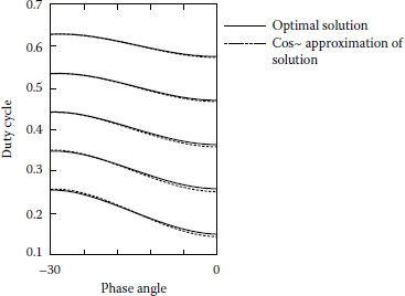
FIGURE 13.12 Results for the duty cycle modulation for the same phase as in Equation 11.3. (From Neacsu, D.O., Yao, Z., and Rajagopalan, V. IEEE PESC Conference, June 1996, Baveno, Italy, 24–27, pp. 727–732, IEEE Paper 0-7803-3500-7/96. © (1986) Printed with permission from IEEE.)
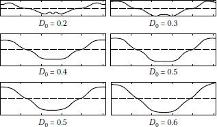
FIGURE 13.13 Input current theoretical waveform: solid line, without modulation; dashed line, with modulation. (From Neacsu, D.O., Yao, Z., and Rajagopalan, V. IEEE PESC Conference, June 1996, Baveno, Italy, 24–27, pp. 727–732, IEEE Paper 0-7803-3500-7/96. © (1986) Printed with permission from IEEE.)
Notice a linear dependence of the amplitude of the cosine modulation waveform on the switch duty cycle. The amplitude is given by this linear dependence, whereas the phase variation is achieved with a phase locked-loop (PLL)-based circuit for synchronization with input line voltages. The modulation wave thus obtained is used with a classical PWM integrated circuit (IC) to control the switch.
Taking into account the power conservation principle can help demonstrate that each 2nth harmonic in the power converter’s output voltage is related to the input current harmonics of orders 2n + 1 and 2n − 1 (output constant load, input symmetrical system). For instance, an action against the 6th harmonic in the output would also minimize the effect of both 5th and 7th harmonics in the input current.
Injection of a harmonic signal within the reference for the PWM control is able to correct the ideal low-frequency shape of the input current. Figure 13.13 presents theoretical low-frequency components for the cases with and without harmonic injection.
The actual input current harmonics are also influenced by the input filter. One of the negative effects of the input filter that adds up to delays in the control system and the effect of the sampling interval is the phase shift between the input voltage and current. To compensate for this phase delay, a small phase shift should be considered within the harmonic injection reference.
Figures 13.14 and 13.15 show harmonic results when this solution is considered within a power converter-based grid interface. The THD of the input current is still above 5%, but Figure 13.14 does not include the effect of the input filter. The remaining harmonics are at higher frequencies, and they can be removed with a conventional low-pass filter. As the optimal PWM reduces the content in the low frequencies, 5th and 7th harmonics of the input current for the case without harmonic injection and for the case with harmonic injection are shown in Figure 13.15. It can be seen that the cumulative effect of both 5th and 7th harmonics is reduced by this approach: (min(V52 + V72)). For a switching frequency of 5 kHz, the content in low harmonics for the case without optimal modulation is I5 = 6.77% and I7 = 1.01%, whereas the case with optimal PWM leads to I5 = 3.84% and I7 = 3.83%. However, both harmonics are inside the limits imposed by IEC 555-2 (I(5) = 1.14A and I(7) = 0.77A) for the output powers in the kW region. For D > 0.5, the content in both harmonics is less than 4% as required by IEEE 519-1992.
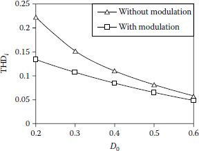
FIGURE 13.14 THD for input current over the switch duty cycle computed with the first 500 harmonics. (From Neacsu, D.O., Yao, Z., and Rajagopalan, V. IEEE PESC Conference, June 1996, Baveno, Italy, 24–27, pp. 727–732, IEEE Paper 0-7803-3500-7/96. © (1986) Printed with permission from IEEE.)
The harmonic injection in the PWM reference signal of a single-switch three phase PWM boost converter has the following advantages:
• Reduced instability risk due to discontinuous conduction mode;
• Applicable to the single-switch three-phase boost converter topologies (including the modern resonant ones) with minimal and low-cost modifications of the command circuit;
• Implementation with any conventional PWM IC owing to the operation with constant switching frequency;
• Reduced requirements for the mains filter and enlarged domain of having input THD current less than 5% and input power factor greater than 95%.
Many applications require a bidirectional power transfer to the grid, and this implies moving the boost power converter stage closer to the grid without the intermediate stage of diode rectification. Figure 13.16 shows the three-phase six-switch power converter. Chapter 3 introduced this power stage with applications to DC/AC conversion and AC motor drives. The same power converter with a different control is the most important three-phase electronic grid interface [14,15,16].
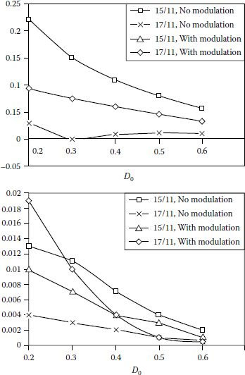
FIGURE 13.15 Low harmonics content of the input currents. (From Neacsu, D.O., Yao, Z., and Rajagopalan, V. IEEE PESC Conference, June 1996, Baveno, Italy, 24–27, pp. 727–732, IEEE Paper 0-7803-3500-7/96. © (1986) Printed with permission from IEEE.)
This topology allows a bidirectional power flow with the control of both the DC bus voltage and the input power factor, although the input currents have low harmonics [17,18,19,20,21,22,23]. This ensures a very high performance interface to the grid for different industrial equipment, such as electrical drives or DC load supply. Electrical drives with AC/DC boost bridge converters also benefit from energy savings during braking or acceleration during drive dynamics. Controlling the DC bus voltage allows capacitor discharge into the grid instead of on a dummy brake resistor (Figure 13.16).
Let us develop a mathematical model for the analysis of this power converter starting from the grid electrical circuit. The grid voltages are defined as:
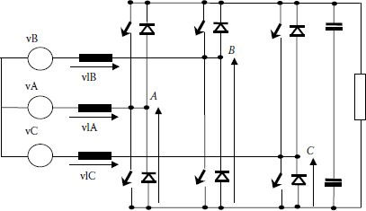
FIGURE 13.16 Three-phase grid interface with six switches.
(13.15) |
The voltage equations for each phase can be expressed in dependence with the each pole voltage from the power converter.
ea0=Rr⋅i1a+Lr⋅di1adt+va0eb0=Rr⋅i1b+Lr⋅di1bdt+vb0ec0=Rr⋅i1c+Lr⋅di1cdt+vc0 |
(13.16) |
The first approach to the analysis of this converter was developed with a scalar control of the DC voltage through the modulation index of the PWM references synchronized with the AC grid voltage [24]. The difference between the fundamental of the voltage generated by PWM and the grid voltage is applied to the boost inductance, defining the input currents. Given the inherent phase shift produced by an inductor, the control references should be appropriately shifted and synchronized.
A second approach consisted of the so-called delta control of the power converters [25], which is an equivalent of the hysteresis control method.
Later on, vectorial methods [9,10,11,12,13] were preferred for control of this power converter [13,26,27]. The vectorial methods for three-phase systems have been presented in Chapter 5 for DC/AC converters and they can be extended to AC/DC conversion. They provide high performance current control in the d–q frame and have the particular advantage of separating the active and reactive power components. As one of the most important requirements for the grid interfaces is the unity or controllable power factor, this features become very important.
The three-phase system of equations from Equation 13.16 can be transformed in an equivalent two-phase system expressed by:
(13.17) |
The transformation of these equations into the synchronous reference frame
(13.18) |
yields the input voltage equations in the synchronous d–q reference frame
(13.19) |
The grid voltages are expressed by two constant components:
(13.20) |
Equations 13.19 and 13.20 demonstrate that the grid current can be decomposed into two components:
• iq allows the control of the input reactive power.
• id allows the control of the input active power.
Working with unity power factor means to keep iq = 0. The id current reference is many times provided by the output of a proportional-integral (PI) controller for the DC bus voltage control (Figure 13.17), as this component has the role of active power transfer to the DC bus.
The module Compensation, Voltage limit, and Transform will be explained later in this chapter. The PWM module has to transform the reference voltage orthogonal coordinates into six gating signals for the power devices. A previous chapter for PWM algorithms showed several solutions for the DC/AC conversion. All of them can be redesigned for the grid interface application as they can be reduced to a set of reference voltages to be transformed into gate pulses. A group of methods are based on a conversion from the orthogonal system in phase reference voltages followed up by a comparison with a carrier waveform.
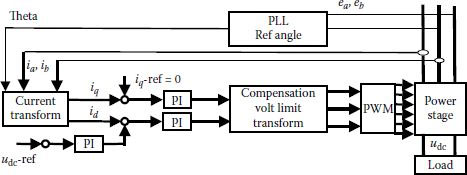
FIGURE 13.17 Base control structure.
The space vector PWM concept allows better utilization of the DC bus voltage compared to carrier-based PWM methods and it represents, hence, a most convenient selection. The maximum voltage achievable at the power converter input is:
(13.21) |
It is important to be able to have a large input voltage for the dynamic range of the system. The more the voltage is available to be applied to the boost inductors, the faster the transients can be achieved. Full analysis of the closed loop options is later included.
According to this SVM method, any set of instantaneous three-phase voltages can be obtained by switching the inverter between six active states defining the six-step operation and the null states in order to approximate a uniform rotation of the space vector corresponding to the three-phase input voltage system. Any desired position of the space vector in the complex plane is calculated by weighed addition of the neighboring switching vectors.
After the time intervals have been defined, there are several possibilities to distribute the active states over the sampling period. An interesting alternative does not switch each device for 60° on each fundamental cycle. This has also been discussed in Chapter 4 for generic PWM algorithms. As the input-phase current should be in phase with the input-phase voltage, the 60° no-switching interval should be chosen around the inverter-switching vectors (Figure 13.18). The main waveforms corresponding to this operation are presented in Figure 13.19.
13.2.3 TOPOLOGIES WITH CURRENT INJECTION DEVICES
Power electronics technologies are nowadays used for higher and higher power level applications. Higher power delivery is achieved on three-phase systems rather than single-phase systems. The design engineer faces thus an important trade-off between the standard requirements for harmonic reduction in three-phase systems and the cost reduction with keeping low the power installed in electronics. A compromise solution relies in using a combination of a high power diode rectifier and low-power compensation equipment [28]. The simplified idea of an active filter is shown in Figure 13.20.
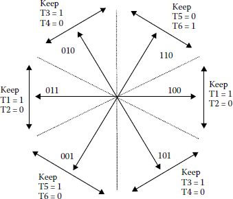
FIGURE 13.18 Switching vectors and definition of the no-switching intervals.
FIGURE 13.19 Waveforms characterizing the modulation with no-switching for 60° over a fundamental cycle.
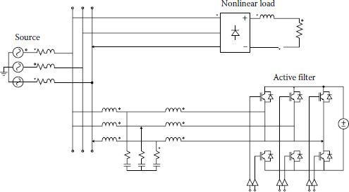
FIGURE 13.20 Principle of an active filter.
The idea of adding up a compensation current to the diode rectifier’s input current has been further exploited with the proposal of simplified passive injection circuits. It is worthwhile to mention here the work of Mohan et al. in early 1990s [29,30]. The core idea was to detect a 3rd harmonic current from the load side and to inject this current into all the input currents as a zero sequence component (Figure 13.21). They used a specially constructed magnetic device able to create the three identical third harmonic currents to be added to the input currents. Other similar principle solutions were reported in [31] and they consisted of a pure R-L-C network tuned on the third harmonic and able to depict this harmonic component for injection into the rectifier’s input currents. The injection network sent a third harmonic current of 0.50*I into each phase, that circulated through the conducting diodes as a 0.75*I current, to add up from both DC+ and DC− into a 1.50*I current at node N. The phase without conducting rectifier diode had the 0.50*I current projected directly into the grid, while the phases with conducting diodes had seen the load current plus the 0.25*I. Improvements to these waveforms became possible with optimized control.
Later on, the advances in power semiconductor technology and the control (Figures 13.22 and 13.23) circuitry allowed the efficiency improvement with the use of active injection circuits [32] (Figure 13.24). Their operation is similar to the original principle of active filtering (Figure 13.25).
There is a large variety of other passive and active injection circuits, and the above circuits are shown for illustration only.
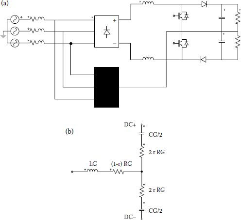
FIGURE 13.21 Principle of current injection.
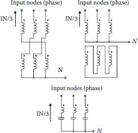
FIGURE 13.22 Third harmonic current injection with passive circuits.
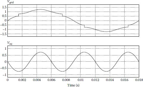
FIGURE 13.23 Injection current and grid current for circuit of Figure 13.22.
FIGURE 13.24 Active current injection circuits.
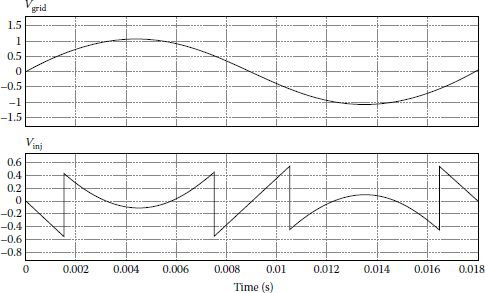
FIGURE 13.25 Injection current and grid current for circuit of Figure 13.24.
13.3 CLOSED-LOOP CURRENT CONTROL METHODS
As shown in Figure 13.17, the most important module of the control system consists of the closed-loop current controllers. The model of the system is expressed by Equation 13.19 and PI controllers are considered on each axis. As Equation 13.19 is different for each axis, different approaches to compensate the cross-coupling terms are considered. Such terms are considered within the following module at the output of the PI current controller.
The PI current loop should be mainly designed to compensate the load voltage produced by the boost inductance term of Equation 13.19. A schematic representation is given in Figure 13.26.
There are many methods to define the gains for the PI control and they are reviewed in Chapter 9. A simplified approximation is given here based on the boost circuitry parameters. The condition of unity gain of the closed-loop transfer function leads, after some calculation, to the values of the PI gains:
• Gain of the integrative term
(13.22) |
• Gain of the proportional term
(13.23) |
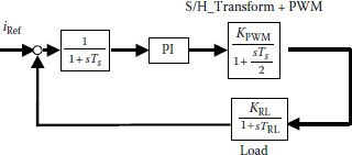
FIGURE 13.26 Schematics of the PI control system.
The concept of the vectorial control of three-phase power converters has already been discussed in Chapter 5. The application to grid interface systems encounters some limitations in the transient response performance due to limited voltage available across the boost inductance. A derivative of a direct application of the PI control without any special compensation is that the transient response time for input current step-up is shorter than the transient response time for the current step-down and the latter can be bothersome in many cases.
13.3.3 TRANSIENT RESPONSE TIMES
On the basis of PI gains, one can calculate the minimum response time for step-up or step-down transitions. As the resistive component is very small, the term Rri can be even neglected. Owing to the largely inductive character of the load, a fast transient of the active current can be achieved with a large voltage applied across the boost inductance.
As the first equation in Equation 13.19 contains the E term, there are two different cases for analysis depending on the sign of the current change:
• Step-up: In order to increase the active current (id), it is necessary to provide the minimum available voltage across Lr (Figure 13.27). The response time will be small and it yields:
(13.24) |
• Step-down: In order to decrease the active current (id), it is necessary to provide the maximum available across Lr. The response time yields:
(13.25) |
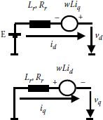
FIGURE 13.27 Equivalent circuits for d and q axis.
13.3.4 LIMITATION OF the (VD,VQ) VOLTAGES
It is easy to notice that different step-up and step-down time intervals are achieved with a smaller value for the step-up transient time. The step reference to the PI controller will have the tendency to force the output of the controller at a higher than possible value. Usually, a software limitation block is included as presented in Figure 13.28. This figure also illustrates the PI implementation in the context of Equation 13.19. The cross-coupling terms and the E term are also included. The cross-coupling terms are taken from the current feedback, but an alternative would be the reference currents.
It is important to note that many implementation solutions of the PI control of the grid interface converter use control systems similar to the motor control ones, without the term E. The problem with such an approach is that the dynamic range at the output of the PI controller is limited further by working with the voltage vd component always close to the E value. The digital range for voltage may also be close to the value of E and the output of the PI controller may saturate digitally by reaching the end of its range. Figure 13.29 shows results for the control structure defined with Figure 13.28.
A multitude of solutions is reported in the technical literature to overcome this problem by artificially augmenting the voltage available to be applied across the input boost inductor [33,34]. Observing Figure 13.27 and Equation 13.19 defines two easy approaches to increase the maximum available voltage at the converter input:
• Using the cross-coupling terms.
• Overlooking the PI outputs and applying all the maximum available voltage during transients.
13.3.5 MINIMUM TIME CURRENT CONTROL
The minimum time current controller leads to excellent performance by finding the optimal control voltage to track the reference current with minimum time based on the optimal control theory. However, the applicability of this method is jeopardized by the large computational burden. The minimum time current controller is very similar to the following solution that will be discussed in more detail.
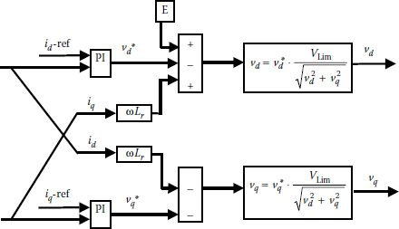
FIGURE 13.28 Schematic of the usual control with limitation.
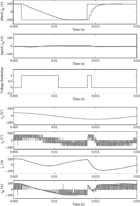
FIGURE 13.29 Simple current controller with voltage limitation for Lr = 2.5 mH, Rr = 0.1 V, Vdc = 570 V, E = 220 V, f = 50 Hz. (From Neacsu, D.O. IEEE International Symposium on Industrial Electronics, Bled, Slovenia, July 1996, 12–14, pp. 527–553. IEEE Paper 0-7803-5662-4/99. © (1996) Printed with permission from IEEE.)
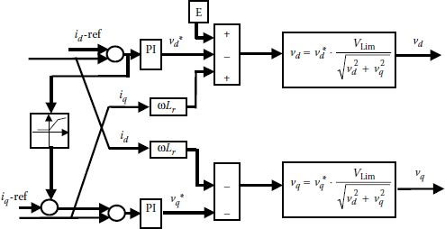
FIGURE 13.30 Schematic of the control system using cross-coupling terms.
The cross-coupling term (ω·Lr·iq) [34] of Equation 11.19 is used to increase the voltage capability by increasing the iq-axis current during a step in the active current id. In this case, the iq current is used to maximize the applied voltage on the inductance Lr. Pushing a high iq current while respecting i2q+i2d≤id max can increase the term (ω·Lr·iq) and improve the voltage capability on the active current (id) axis. The unity power factor is given up during transients.
The increase in voltage can be expressed as:
(13.26) |
Results for step-up and step-down transients of the active current while applying the method shown in Figure 13.30 are shown in Figure 13.31.
Changing the iq current reference or working with current on the q axis requires voltage to be applied on this axis (vq). As the maximum available voltage is at any moment limited by the maximum radius of the space vector trajectory in the complex plane, a voltage applied on the q-axis may reduce the maximum voltage available on the d-axis, and this jeopardizes somewhat the merits of this method. For this reason, an alternative is next analyzed by applying all voltage on the d-axis and suspending temporarily the effect of the PI control at large current errors.
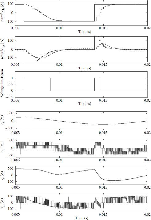
FIGURE 13.31 Current controller with d–q axis cross-coupling for the case Lr = 2.5 mH, Rr = 0.1 V, Vdc = 570 V, E = 220 V, f = 50 Hz. (From Neacsu, D.O. IEEE International Symposium on Industrial Electronics, Bled, Slovenia, July 1996, 12–14, pp. 527–553. IEEE Paper 0-7803-5662-4/99. © (1996) Printed with permission from IEEE.)
13.3.7 APPLICATION OF the WHOLE AVAILABLE VOLTAGE ON the d-AXIS
The limit of the maximum available voltage is generally expressed as
(13.27) |
When applying all the voltage on the d-axis, vd = Vlim, vq = 0 and the q-axis current is negative from Equation 13.19, will further help increasing the d-axis voltage.
Re-writing Equation 13.19 for the case presented in Figure 13.32 and neglecting the voltage drop across the resistance in the boost circuitry yields:
(13.28) |
Solving this system yields the solutions:
id(t)=Id⋅ cos ωt−Vlim−Eω⋅Lr⋅ sin ωtiq(t)=−Id⋅ sin ωt+Vlim−Eω⋅Lr⋅(1− cos ωt) |
(13.29) |
The response time for a step-down transient from Id to 2Id can be calculated by imposing the condition id (ΔT) = −Id. Figure 11.27 presents a theoretical response without taking into consideration the sampling effect.
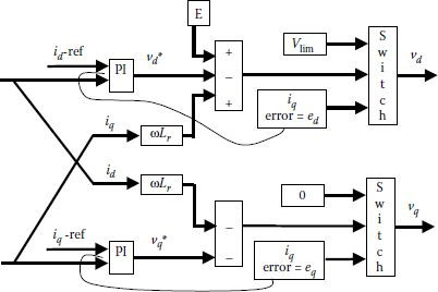
FIGURE 13.32 Control schematic for a system with application of the whole available voltage on d-axis during transients.
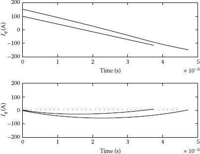
FIGURE 13.33 Theoretical response at id current step-down (100 A to −100 A and 150 A to −150 A) for Lr = 2.5 mH, Rr = 0, Vdc = 570 V, Vlim = 0.61 * Vdc, E = 220 V. (From Neacsu, D.O. IEEE International Symposium on Industrial Electronics, Bled, Slovenia, July 1996, 12–14, pp. 527–553. IEEE Paper 0-7803-5662-4/99. © (1996) Printed with permission from IEEE.)
It is very interesting to note that a step-down current modification from Id to 2Id brings iq back to zero, and this will not jeopardize the behavior of the iq current controller when this is again engaged (Figure 13.33) [27].
Figure 13.34 shows results for the application of the entire voltage on d-axis during a transient. A comparison can be made with Figures 13.29 and 13.31. At larger values of the id current, applying the whole available voltage on the active current axis leads to better results. As discussed before, the solution involving the cross-coupling terms requires some voltage on the q-axis to form the current iq and the remaining voltage on the d-axis is reduced. Furthermore, asking for step modifications in both axes can produce instabilities during and following a transient.
13.3.8 SWITCH TABLE AND HYSTERESIS CONTROL
Fast current transients can be achieved with hysteresis control instead of PI control. Accounting for the symmetries within the three-phase systems, hysteresis control is considered for the two orthogonal (x, y) components of the grid current.
A novel hysteresis method in the synchronous reference (d, q) is introduced in Figure 13.35 and Table 13.2. The major advantage of this method, in comparison with the conventional stationary reference for the hysteresis control, consists in its simplified implementation in vector-control systems. Current double-level hysteresis control in (d, q) axes produces logic signals (yd, yq) that can uniquely be converted in (vd, vq) components of the voltage at the converter input. The sampling frequency can also be limited. The switch table is employed to select the switching vector closest to the coordinates (vd, vq) resulting from this algorithm (Figures 13.36 and 13.37). As an alternative, this method can be applied with or without employing the cross-coupling terms. In a sense, this method is the equivalent of direct torque control used for the AC machine drives.
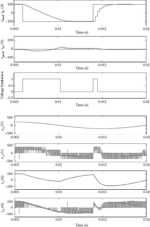
FIGURE 13.34 Whole voltage on d-axis for the case Lr = 2.5 mH, Rr = 0.1 V, Vdc = 570 V, E = 220 V, f = 50 Hz. (From Neacsu, D.O. IEEE International Symposium on Industrial Electronics, Bled, Slovenia, July 1996, 12–14, pp. 527–553. IEEE Paper 0-7803-5662-4/99. © (1996) Printed with permission from IEEE.)
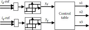
FIGURE 13.35 Schematics of the hysteresis control in synchronous frame.
13.3.9 PHASE CURRENT TRACKING METHODS
Single- and three-phase grid connected power converters can also be controlled in a stationary reference frame directly employing phase or sinusoidal currents. The current control system reduces to a PI controller with a sinusoidal reference (Figure 13.38). Unfortunately, this type of system has been proven to introduce a nonzero steady-state error. To mitigate this issue, a solution based on an internal model principle [35] is discussed.
Let us consider a sinusoidal reference
(13.30) |
with the Laplace transform
(13.31) |
TABLE 13.2
Switching Table (θ Represents the Angle of the Grid Voltages)
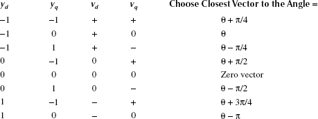
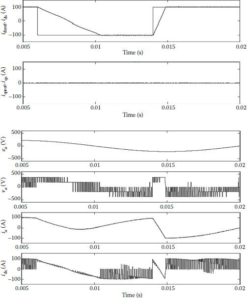
FIGURE 13.36 Switch table and hysteresis control for the case Lr = 2.5 mH, Rr = 0.1 V, Vdc = 570 V, E = 220 V, f = 50 Hz. (From Neacsu, D.O. IEEE International Symposium on Industrial Electronics, Bled, Slovenia, July 1996, 12–14, pp. 527–553. IEEE Paper 0-7803-5662-4/99. © (1996) Printed with permission from IEEE.)
The Laplace transform for the error signal can be expressed as:
(13.32) |
where G0(s) represents the open-loop transfer function of the control system.
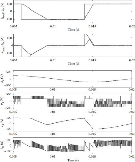
FIGURE 13.37 Switch table and hysteresis control using cross-coupling terms for the case Lr = 2.5 mH, Rr = 0.1 V, Vdc = 570 V, E = 220 V, f = 50 Hz. (From Neacsu, D.O. IEEE International Symposium on Industrial Electronics, Bled, Slovenia, July 1996, 12–14, pp. 527–553. IEEE Paper 0-7803-5662-4/99. © (1996) Printed with permission from IEEE.)
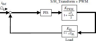
FIGURE 13.38 Schematics of the PI control system.
We would like to find the optimal form of the open-loop transfer function able to cancel the effect of the two imaginary poles (+/− jω0) introduced by the sinusoidal reference term. In this respect, the open-loop transfer function is written as a ratio of polynomials with real number coefficients.
(13.33) |
D(s) = 0 should have the same solutions (+ / − jω0) in order to cancel the effect of the sinusoidal reference. Moreover (+ / − jω0) should not be at the same time solutions of N(s) = 0. This guarantees the elimination of the complex number solutions and the reduction of the steady-state error to zero.
The implementation of this control method is shown in Figure 13.39. The conventional PI regulator is enhanced by a term corresponding to the two imaginary solutions (+ / − jω0).
The equivalent transfer function of the regulator becomes:
GPIS(s)=Kp+Kis+Ks⋅ss2+ω20=Kp⋅s⋅[s2+ω20]+Ki⋅[s2+ω20]+Ks⋅s2s⋅[s2+ω20] |
(13.34) |
The open-loop transfer function is calculated as:
(13.35) |
(13.36) |
and
(13.37) |
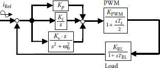
FIGURE 13.39 Block diagram of the compensated controller.
E(s) has no imaginary poles introduced by the sinusoidal reference. It can be observed that (+ / − jω0) are imaginary poles of G0(s) as proposed by the new control algorithm.
13.3.9.2 Feed-Forward Controller
The control method previously named as Proportional-Integrative-Sinusoidal is currently very much used in controlling currents of both grid interactive and active filtering applications. Improved forms are proposed in [36,37], as well as a H∞ application. We can also mention a variation of these controllers used for higher harmonic cancelation [38]. The main drawback of this method consists in its dependency on the accurate knowledge of the grid frequency as this is part of the control law. If the grid frequency slightly changes, it yields in a steady-state error of the tracking system (Figure 13.40).
Observing that the current controller acts upon an inverter leg that is composed of two IGBT devices, one can separate the operation on the positive and negative polarities of the current with independent control of each power device. This yields into the control system shown schematically in Figure 13.41.
The control problem changes from tracking a sinusoidal waveform (harmonic, periodic) waveform, into tracking [occasionally] a varying waveform [39]. The intervals with a null reference would reset the steady-state error if any. We can thus consider the reference as approximating a piece-wise waveform, and following up a control system design similar to the case of a ramp input (also called “velocity” input) [40].
The reference input is equivalent to
(13.38) |
with the Laplace transform
(13.39) |
In order to achieve one additional degree of freedom on the zero assignment within the control law, a feed-forward component is added to compensate nonideal behavior of the control loop under varying input waveform (Figure 13.42).
The controller output yields:
CPIFF(s)=(Kp+Kis)⋅(IR(s)−Im(s))+Kn⋅IR(s)Im(s)=CPIFF(s)⋅GINV(s)⋅GLOAD(s) |
(13.40) |
It yields:
(13.41) |
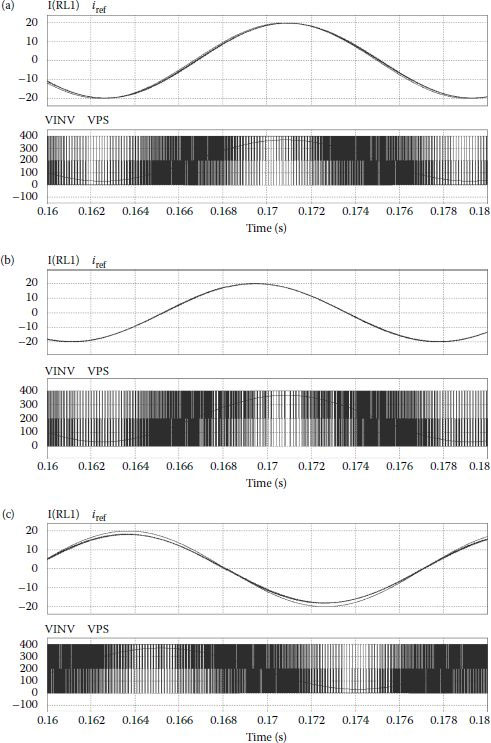
FIGURE 13.40 Results for different control methods: (a) Conventional PI controller, (b) PI + Resonant, (c) PI + Resonant out of synchronism (grid at 56 Hz instead of 60 Hz). Top waveform = Phase current reference and measurement. Bottom waveform = Inverter pole voltage and grid voltage.
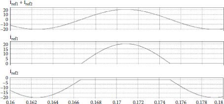
FIGURE 13.41 Principle of the control system.
And finally
E(s)=IR(s)−Im(s)=[1−Kn⋅GINV(s)⋅GLOAD(s)1+(Kp+Kis)⋅GINV(s)⋅GLOAD(s)]⋅IR(s) |
(13.42) |
The Final Value Theorem is applicable since there is no right-half pole and the steady-state error yields:
ess=limt→∞e(t)=lims→0s⋅E(s)==lims→0{s⋅[1−Kn⋅GINV(s)⋅GLOAD(s)1+(Kp+Kis)⋅GINV(s)⋅GLOAD(s)]⋅IRs2}=lims→0{[1−Kn⋅K1s+K2]⋅[ss+GK0]⋅IRs}=0 |
(13.43) |
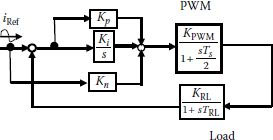
FIGURE 13.42 Feed-forward controller.
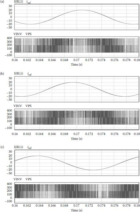
FIGURE 13.43 Results for novel concept. (a) The use of two conventional PI controllers, (b) the use of the feedforward component, (c) same as b, with grid at 56 Hz instead of 60 Hz. Top waveform = Phase current reference and measurement. Bottom waveform = Inverter pole voltage and grid voltage.
Sample results are shown in Figure 13.43. It shows the improvement from Figure 13.40 when the grid frequency varies. It is also important to note the role of proper synchronization of the operation with the grid.
More experimental results are shown in [40]. The performance of the feed-forward controller is comparable with the performance of the proportional-integral-sinusoidal controller (also called resonant controller). In certain implementations like the analog power management ICs, the system is simpler than the resonant controller. This is especially evident for compensation of currents with multiple harmonic components.
Advantages in improved power efficiency and faster transient response are achieved with the split of the control action on the two IGBT composing an inverter leg and the operation of the power switches for 180° only. This means reduction of the power loss, especially in the control and driver circuits.
Grid-connected power converters are seen as a current source by the grid while the input voltages are defined by the grid. This implies a synchronization of the PWM pattern with the phase of the grid in order to control the power factor. There are different methods based on a PLL circuit that are used to achieve grid synchronization.
The simplest solution used to synchronize the control of a single-phase grid connected power converter consists in a zero-crossing detector followed by a counter circuit (Figure 13.44).
The grid voltage is sensed before any filter associated with the power converter and reduced to a lower level with a signal transformer or resistive divider. The resulting signal is compared against a threshold device, such as the base-emitter junction of a bipolar transistor or an IC comparator. This provides a logic signal corresponding to the alternating of the grid voltage. There are several sources of errors in this detection, including the noise in the line voltage due to unfiltered switching, dispersion and temperature variations of the threshold level, or delay in detecting the exact zero-crossing moment. However, these errors are generally smaller than the quantization step of the digital system.
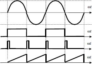
FIGURE 13.44 Principle of a simple synchronization circuit.
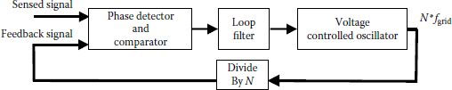
FIGURE 13.45 Principle of a PLL circuit.
The edges of the detected logic signal reset a digital counter that accounts for the phase coordinate of the PWM pattern. Improved systems include a phase-locked loop configuration able to filter unwanted small variations in the detecting process. This helps eliminating the jitter around the zero-crossing moments.
Let us consider a synchronization scheme based on a PLL circuit. A generic PLL circuit schematic is shown in Figure 13.45 and it is composed of a voltage-controlled oscillator (VCO) working at a frequency multiple of N times the detected frequency. In power converters, it makes sense to select the VCO frequency equal to the sampling frequency of the PWM pattern (Figure 13.46). The resulting train of pulses is divided by N resulting in a logic signal with a frequency comparable with the sensed voltage. A phase detector compares the phase of the sensed and feedback voltages and it increases or decreases the control voltage accordingly. This control voltage is used as a reference for the VCO that modifies its frequency based on the phase difference. The goal of this closed-loop approach is to align the sensed signal with the generated one. If the frequency or phase of the sensed signal varies for any reason, this control loop acts as a filter and the feedback signal does not jitter. The feedback signal can further be used as a reference for the generation of the PWM pattern. Usually, the same counter is used both for closing the PLL loop and for counting the angular coordinate of the PWM pattern.
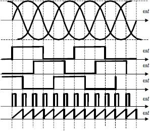
FIGURE 13.46 Principle of a simple synchronization circuit.
The major problem people face when implementing this PLL control in single phase systems relates to the limited number of PWM cycles within one grid period. The discrete nature of the PWM-generation process limits the possibility of adjusting properly the controller phase. For instance, a converter with a 9 kHz switching frequency allows for 150 steps in the phase coordinate. The decision of the feedback loop can only be to adjust the phase by ±1 PWM pulse at a time. The effect is a possible step in the filtered voltage at each zero crossing when the phase is abruptly reset to zero. An alternative consists in using asynchronous PWM generators, but they do not guarantee the best harmonic content of the grid current. However, evolved systems can afford to work with asynchronous PWM that allows a noninteger ratio of switching and grid frequencies.
The PLL function can be implemented with dedicated analog or digital ICs or a proper software routine in the microcontroller or digital signal processor (DSP) control system. The frequency of the main signal is 50 or 60 Hz, which is very low compared to the performance of modern digital controllers. Therefore, a microcontroller implementation requires a zero crossing detector with direct interface to the digital hardware, a timer/counter counting with the clock frequency of the PWM sampling frequency, and a software routine running at the same sampling frequency.
Grid synchronization for three-phase converters benefit from multiple zero crossings and the symmetry of a grid generated three-phase system. The detection module includes zero-crossing detection for all three phases, and this results in a signal with a frequency six times larger than the grid frequency. The PLL circuit can therefore provide more resolution with a much finer tuning of the detected frequency.
Again the implementation can be achieved with analog or digital PLL ICs or with a software routine in the digital controller system.
P13.1 |
Calculate the average and RMS values for the output voltage of rectifier systems shown in Table 13.1. |
P13.2 |
What is the effect of a line or grid inductance in the commutation process of the converter shown in Figure 13.2. |
P13.3 |
Draw the switching pattern of the GTO devices of Figure 13.3c to obtain the output voltage waveforms shown for both cases. How would you define the semiconductor loss for both control methods? |
P13.4 |
Consider the two topologies shown in Figure 13.7. What happens if the intermediate DC capacitor is missing? What should be the minimum value of this capacitor to maintain the operation as desired? |
P13.5 |
Compare the rating of the rectifier diodes in both solutions of Figure 13.8. |
P13.6 |
Compare the input filter-capacitor rating for the two solutions shown in Figure 13.10. |
P13.7 |
Following the example provided by Equations 13.3, 13.4, 13.5, 13.6, 13.7, 13.8, 13.9, 13.10, 13.11, 13.12, 13.13, calculate the shapes of the current in the much simpler case of a single phase converter and justify the second harmonic injection. |
P13.8 |
Compare the ratings of the IGBT devices used in building the power converters shown in Figure 13.11 and Figure 13.16, respectively, for the same grid-and-load conditions (say, 2 kW with a 120 V/60 Hz grid). |
P13.9 |
What are the drawbacks of neglecting the term E in the control system shown in Figure 13.22? Many people adapt their DSP control software from a motor drive application to a grid-connected converter without adding up this term. The system apparently works, but at what risk? Can you complete this response with an imaginary example? |
P13.10 |
Determine the reasoning behind the switching sequence shown in Table 13.2 by using a vector diagram for both current and voltage. |
P13.11 |
Usually, practical systems of single-phase tracking control do not compensate for the sinusoidal reference. The system apparently works, but at what risk? Can you complete this response with an imaginary example? |
P13.12 |
Consider a single-phase grid-connected converter switched at 3.6 kHz, that is, a frequency ratio of 30. If the PWM generator maintains the synchronization between the generated PWM pattern and zero crossing, how big can be the steps in filtered voltage (or in the voltage reference for the PWM) at each zero crossing reset? |
1. Anon. 1998. Ecostar—Power converter anti-islanding capability. Application Notes, Ballard Corporation.
2. Anon. Ecostar—Power converter designed for distributed generation. Application Notes, Ballard Corporation.
3. Anon. 1998. Ecostar—Multi-unit capability for grid and standalone operation. Application Notes, Ballard Corporation.
4. Chiang, H.D., Wang, J.C., Tong, J., and Darling, G. 1995. Optimal capacitor placement, replacement and control in large scale unbalanced distribution systems: System modeling and a new formulation. IEEE Trans. Power Syst. 10(1), 363–369.
5. Anon. 2001. PV system installation and grid interconnection guidelines in selected IEA countries, Fronius.
6. Anon. 2003. IEEE standard. IEEE P1547 std draft 01 standard for distributed resources interconnected with electric power systems. June 2003.
7. Prasad, A.R., Ziogas, P.D., and Manias, S. 1989. An active power factor correction technique for three-phase diode rectifiers. IEEE PESC Conference Record, pp. 58–66.
8. Kolar, J.W., Ertl, H., and Zach, F.C. 1993. A comprehensive design approach for a three-phase high-frequency single-switch discontinuous-mode boost power factor corrector based on analytically derived normalized converter component ratings. IEEE IAS Conference Record, Part II, pp. 931–938.
9. Kolar, J.W., Ertl, H., and Zach, F.C. 1993. Space vector-based analytical analysis of the input current distortion of a three-phase discontinuous-mode boost rectifier system. IEEE PESC Conference Record, pp. 696–703.
10. Tou, M., Al-Haddad, K., Olivier, G., and Rajagopalan, V. 1995. Analysis and design of single controlled switch three-phase rectifier with unity power factor and sinusoidal input current. IEEE APEC Conference Record, vol. II, pp. 856–862.
11. Ismail, E., Olivieira, C., and Erikson, R. 1995. A low-distortion three-phase multi-resonant boost rectifier with zero current switching. IEEE APEC Conference Record, vol. II, pp. 849–855.
12. Weng, D. and Yuvarajan, S. 1995. Constant-switching-frequency AC–DC converter using second-harmonic-injected PWM. IEEE APEC Conference Record, vol. II, pp. 642–646.
13. Weng, D. and Yuvarajan, S. 1995. AC–DC converter using second-harmonic-injected PWM. IEEE PESC Conference Record, vol. II, pp. 1001–1006.
14. Malesani, L., Rossetto, L., Tenti, P., and Tomasin, P. 1993. AC/DC/AC PWM converter with minimum storage energy in the DC link. IEEE APEC Conference Record, pp. 306–313.
15. Verdelho, P. and Soares, V. 1997. A unity power factor PWM voltage rectifier based on the instantaneous active and reactive current id-iq method. IEEE International Symposium in Industrial Electronics, July 7–11, pp. 411–416.
16. Habetler, T.G. 1993. A space vector based rectifier regulator for AC/DC/AC converters. IEEE Trans. Power Electron. 8(1), pp. 30–36.
17. Blasko, V. and Kaura, V. 1997. A new mathematical model and control of a three-phase AC/DC voltage source converter. IEEE Trans. Power Electron. 12(1), 116–123.
18. Verdelho, P. and Soares, V. 1997. A unity power factor PWM voltage rectifier based on the instantaneous active and reactive current id–iq method. IEEE International Symposium in Industrial Electronics, July 7–11, pp. 411–416.
19. Trznadlowski, A.M. and Legowski, S. 1994. Minimum-loss vector PWM strategy for three-phase inverters. IEEE Trans. PE 9(1), 26–34.
20. Enjeti, P. and Xie, B. 1990. A new real time space vector PWM strategy for high performance converters. IEEE IAS.
21. Chung, D.W. and Sul, S.L. 1997. Minimum-loss PWM strategy for a 3-phase PWM rectifier. IEEE PESC, 2, 1020–1026.
22. Habetler, T.G. 1993. A space vector based rectifier regulator for AC/DC/AC converters. IEEE Trans. Power Electron. 8, 30–36.
23. Kazmierkowski, M., Dzieniakowski, M.A., and Sulkowski, W. 1991. Novel space vector based current controller for PWM inverters. IEEE Trans. Power Electron. 6, 158–166.
24. Henze, C.P. and Mohan, N. A digitally controlled AC/DC power conditioner draws sinusoidal input current. IEEE PESC, pp. 531–540.
25. Malesani, L., Rossetto, L., Tenti, P., and Tomasin, P. 1993. AC/DC/AC PWM converter with minimum storage energy in the DC link. IEEE APEC Conference Record, pp. 306–311.
26. Neacsu, D.O, Yao, Z., and Rajagopalan, V. 1996. Optimal PWM control of a single-switch three-phase AC–DC boost converter. IEEE PESC, pp. 521–526.
27. Neacsu, D.O. 1999. Vectorial current control techniques for three-phase AC/DC boost converters. IEEE ISIE, pp. 527–532.
28. Kanaan, H.Y. and Al-Haddad, K. 2012. Three-phase current injection rectifiers. IEEE Industrial Electron. Magazine 6(3), 24–40. May/June 2012.
29. Naik, R., Rastogi, M., and Mohan, N. 1992. Third-harmonic modulated power electronics interface with three-phase utility to provide a regulated DC output and to minimize line current harmonics. Proceedings of the IEEE IAS Annual Meeting Conference, pp. 689–694.
30. Mohan, N., Rastogi, M., and Naik, R. 1993. Analysis of a new power electronics interface with three-phase utility currents and a regulated DC output. IEEE trans. Power Delivery 8(2), 540–546.
31. Pejovic, P. and janda, Z. 1999. An analysis of three-phase low harmonic rectifiers applying the third harmonic current injection. IEEE Trans. Power Electron. 14(3), 397–407.
32. Vasquez, N., Rodriguez, H., Hernandez, C., Rodriguez, E. and Arau, J. 2009. Three-phase rectifier with active current injection and high efficiency. IEEE Trans. Industrial Electron. 56(1), 110–119.
33. Choi, J.W. and Sul, S.K. 1998. Fast current controller in three-phase AC/DC boost converter using d–q axis crosscoupling. IEEE Trans. Power Electron. 13(1), 179–185.
34. Choi, J.W. and Sul, S.K. 1997. New current control concept—Minimum time current control in 3-phase PWM converter. IEEE Trans. Power Electron. 12(1), 124–131.
35. Fukuda, S. and Yoda, T. 2001. A novel current-tracking method for active filters based on a sinusoidal internal model. IEEE Trans. Industry Appl. 37, 888–895.
36. Timbus, A., Liserre, M., Teodorescu, R., Rodriguez, P., and Blaabjerg, F. 2009. Evaluation of current controllers for distributed power generation systems. IEEE Trans. Power Electron. 24(3), 654–664.
37. Lisserre, M., Teodorescu, R., and Blaabjerg, F. 2006. Multiple harmonics control for three-phase grid converter systems with the use of PI-RES current controller in a rotating fame. IEEE Trans. Power Electron. 21(3), 836–841.
38. Bojoi, R.I., Griva, G., Bostan, V., Guerrero, M., Farina, F., and Profumo, F. Current control strategy for power conditioners using sinusoidal signal integrators in synchronous reference frame. IEEE Trans. Power Electron. 20(6), 1402–1412.
39. Franklin, G., Powell, D., Emami-Naeimi, A. 2002. Feedback Control of Dynamic Systems. Prentice Hall, Upper Saddle River, NJ.
40. Neacsu, D.O. 2010. Analytical investigation of a novel solution to AC waveform tracking control. IEEE International Symposium in Industrial Electronics, Bari, Italy, July, pp. 2684–2689.
41. Neacsu, D.O., Yao, Z., and Rajagopalan, V. 1996. Optimal PWM control of a single-switch three-phase AC-DC boost converter, IEEE PESC Conference 1996, Baveno, Italy, June 24–27, pp. 727–732.