
2.1 A VIEW ON THE POWER SEMICONDUCTOR MARKET
Power semiconductor components are at the core of any power electronic converter. They have a history of more than 50 years, reach in technology development and market success. Since the technology behind these devices is not new, the differences between the newly released components and the role of these changes are not always easy to understand for a student. For this reason, a brief market survey is herein presented with the goal of outlining why efforts are made for certain performance indices of the power semiconductor devices. It is also important to understand the specifics of the semiconductor industry. Since production is based on large capital equipment, the technology development is done in a cyclical manner.
Power semiconductor devices are at the heart of many modern industrial and consumer end-use applications and come in different size and ratings. The application objectives are ranging from low power supplies of tens of watt to 4 MW locomotives or 10 MW steel rollers.
The power discrete market was estimated at $12.9 billion in 2011, having grown by just over 2% from 2010 [1]. It is worthnoting the continued high demand for discrete IGBTs that accounted for nearly all the growth. This was fuelled by new products for domestic appliances such as room air-conditioning and washing machines targeting especially the Asian markets. Sales of standard power MOSFETs and thyristors declined slightly in 2011 given the limited new development within the economic crisis.
According to IMS Research, the market for power semiconductor modules grew faster than that for discrete power semiconductors in 2010, increasing by 32% to $4.6 billion. The power module market growth was continuing in 2012 despite slowing demand.
The power semiconductor devices most related to our book topic are MOSFET, IGBT, and diverse modern variations of thyristors (SCR). The last 20 years have seen spectacular improvement in technology and performance. The technological S-curves related to the power device capacity are shown in Figure 2.1 [4].
The power MOSFET device was introduced in early 1980s with starting parameters of 3–5 A for the drain current, up to 400 V breakdown voltage and turn-off time in the range of 1.2 ms. Technology development allowed improvement of ratings to different sets of 9 A/600 V or 100 A/50 V and decrease of the turn-off time to 600 ns. The most recent technology advances include the CoolMOS devices that are able to switch 20 A/600 V with a turn-off time of around 100 ns. Among all sorts of MOSFET devices, the largest market increase is now seen in the high current applications where new devices are released continuously.
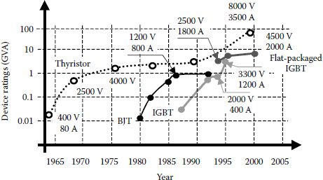
FIGURE 2.1 Technology S-curves with maximum device ratings as parameter.
IGBT devices combine the advantages of bipolar and MOSFET transistors into a device dedicated to power-switching converters operated under high current and high voltage. These devices are the most useful for the class of converters presented in this book, and we will dedicate more space to the presentation of IGBT’s parameters.
The history of IGBTs starts also in early 1980s, but the real technological advent was in late 1980s and early 1990s when several generations of IGBT devices have been developed by a series of companies. Snapshots of performance evolution are next included:
• 1986: starting parameters 50 A/600 V/3 ms
• 1990: commonly from 50 A to 400 A/1000 V/1.8 ms
• 1995: commonly from 50 A to 400 A/1200 V/1.3 ms
• 1996: 800 A/1600 V/1.6 ms
• 1997: 1200 A/3,3 kV/2.2 ms
• 2000: 50 A to 400 A/1200 V/0.4 ms to 0.8 ms
• 2000: 1000 A/3,3 kV are available in smaller series
• 2004: commonly 1000 A/1700 V/1.2 ms, in small series up to 1200 A/6 kV
Given their application to high-power converters, the focus was on the improvement of parameters that relate to the power conversion. During the last 20 years, we have seen technology evolution with effects in
• Current handling capability—increased four times since 1982
• Voltage handling capabilities—increased four times
• Turn-off time dropped 20 times, to around 100 ns today
• Switching frequencies from 2 kHz in early 1980s to 150 kHz in 1999 and 200 kHz nowadays
The evolution of the IGBT market was also impressive over the last 10 years. The 1995 world market for IGBT market was estimated at $200 million, the European market taking the largest share (approximately 45%). The global market increased to $800 million in 2003, and it topped $1 billion in 2005.
All the above performance-related information refers to the limits of the IGBT technology. It is worthlooking also into the market depth. Most of the power converter applications are in lower power range (around kW) rather than the multi-100 kW power range. Also, the production volumes are higher in low kW power range. For instance, there are more inverterized A/C units than locomotives in the world. This explains why the number of vendors and the number of product variations are higher in the lower power range. Figure 2.2 shows a snapshot of all the IGBT product offering of a distributor (digikey) for North American market, in November 2011. It is clearly shown that the most IGBT product types are for 600 V and <50 Amp ratings. Knowing the peculiar aspects of protection and control for these devices covers more applications than focusing on the multi-kW IGBTs. It is true that the companies with products in higher power range also work on direct supplier agreements rather than with distributors.
The success of power semiconductor devices in existing applications and the appearance of new applications encouraged the development of new concepts. Today, emerging high-frequency power semiconductor devices (Example 1–10 kW switched at 100 s kHz) are a very hot R&D topic.
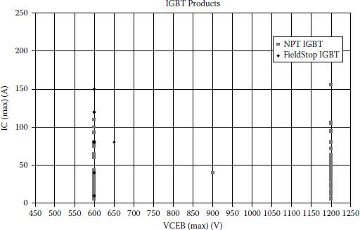
FIGURE 2.2 Cumulative view on the digikey offer for IGBT, on November 2011.
Currently, the discrete power semiconductor devices target the following markets [2]:
• IT and consumer for 33.9%
• Automotive for 12.5%
• Industrial equipment 23.8%
• Consumer appliances 29.8%
The first two categories use mostly lower power devices, and the last two are more related to our book. However, the advent of hybrid electric vehicle (HEV) power electronics is expected to increase the market share of high-voltage automotive applications.
A special market segment refers to the integrated circuits dedicated to power management and motor control. This sector is very dynamic with large investments over the last years.
Power MOSFET devices are faster than bipolar transistors, as they do not have excess minority carrier that should be moved during turn-on and turn-off. A positive voltage is applied at turn-on on the gate circuit. The equivalent gate capacitance is charged through an external gate resistor. When this gate voltage rises above the VGS(th), a current starts circulating in the drain circuit with a (di/dt) determined by both the internal semiconductor structure and the external circuit. During this time interval, charge is stored within both Cds (drain-source) and Cgs (gate-source). This state ends when drain current reaches the level of the current determined by the external circuit (the current is clamped at the load current). As no variation of the current is possible, the voltage across the gate-source circuit remains constant at a level depending on the load-circuit current. This level is called the Miller plateau.
During this state, the gate-source capacitance has a constant voltage, and all the gate current charges the gate-drain capacitance. This determines the trip of the drain source voltage towards the ground. When this voltage reaches a low level, the gate-source voltage increases to the level of the control voltage.
During the first two states of the turn-on transient, electrical charges are moved through the stray capacitances or depletion-layer capacitances, and the equivalent circuit model for transient analysis in cut-off and active regions are shown in Figure 2.3.
The last state shown in Figure 2.4 corresponds to a drain-source voltage VDS < VGS − VGSth, when the MOSFET device enters the ohmic region. In power-switching converters, VGS ≫ VGSth (typically, 15 V > 4 V), and the boundary for the ohmic region is sometimes approximated with VDS < VGS, the equivalent circuit model for the ohmic region (Figure 2.5). The drain-source resistance corresponds to the conduction loss, mostly arising from the drain-drift region. This is the most important performance index for MOSFET devices. Modern MOSFETs go as low as 5 mV RDS(on).
The capacitances Cgd and Cgs are not constant during the transient. A better model can be defined with values varying with the voltage across them. The capacitance Cgd shows a substantial change that can be approximated with a two-step variation (Figure 2.6).
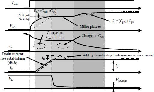
FIGURE 2.3 Generic turn-on waveforms for an IGBT/MOSFET power device.
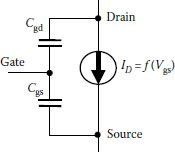
FIGURE 2.4 Model for the transient analysis in cut-off and active regions.
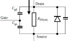
FIGURE 2.5 Model for the analysis of the ohmic region of a MOSFET device.
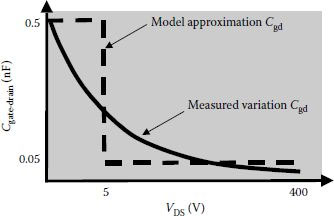
FIGURE 2.6 Variation of the gate-drain capacitance.
The gate-source capacitance is constant on the first interval, increases with voltage on the second interval because of the gate oxide capacitance of drain overlap, and it is constant during and after the third interval. The final value is three to four times higher than the initial value (both values are in the range of few nF).
MOSFET datasheets provide values of CISS, CRSS, and COSS. The following relationships help relate these parameters to inter-junction parasitic capacitances Cgd = CRSS, Cgs = CISS − CRSS, Cds = COSS − CRSS.
The switching speed is not only determined within the input capacitance and gate resistor circuit, but the Miller threshold level and the device transconductance also matter. This is illustrated in Figure 2.7. The first slope (from zero to the Miller threshold) is determined by the input capacitance, which is higher for the second device. However, the second device has a higher transconductance and, therefore, requires less voltage at its gate for a given amount of collector current. The device with the smaller input capacitance is not always faster.
At turn-off, the gate voltage goes to zero and the gate’s equivalent capacitance starts to discharge through the gate resistance (Figure 2.8). Both Cgd and Cgs are discharged at the first interval. When the gate voltage reaches the Miller plateau, it is clamped until the drain voltage increases to the bus voltage. During this interval, charge is changed with the Cgd capacitance only. Finally, the current decreases to zero at the last interval, whereas the drain-source voltage remains at the bus voltage level. The device can be considered turned-off when the gate voltage goes below the threshold voltage. Figure 2.8 also presents the turn-off characteristic of an IGBT device. IGBT devices will be described in the next section. Notice the difference between the MOSFET turn-off with the current tail due to bipolar effect and the use of a bipolar voltage for the gate control.
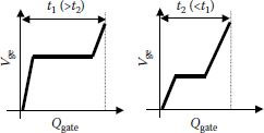
FIGURE 2.7 Gate switching characteristics for two devices.
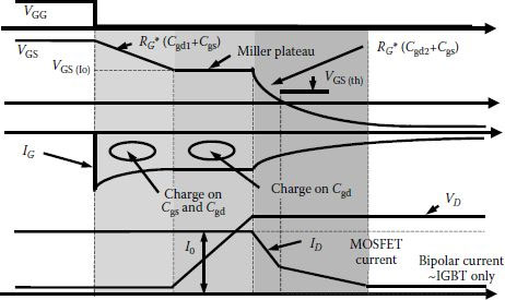
FIGURE 2.8 Generic turn-off waveforms for an IGBT/MOSFET power device.
The MOSFET’s switching characteristics also depend on the external circuit. Switching currents on inductive loads imposes special precautions, including a freewheeling diode for the reactive current (Figure 2.9). As this diode is not an ideal switch, its reverse recovery current has an important influence on the switching characteristics. The dotted lines in both Figures 2.3 and 2.8 illustrate how the reverse recovery current of the free-wheeling diode influences the switching of the power MOSFET.
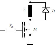
FIGURE 2.9 Using free-wheeling diodes for inductive switching.
There is also another reason for the use of the antiparallel free-wheeling diode. The internal structure of the MOSFET device features a p–n junction between the source and the drain. Under certain conditions, a negative current may free-wheel through this parasitic diode, which may happen especially within an inverter leg when a MOSFET turns off and the other one turns on. The conduction of the parasitic diode becomes a problem because of its slow turn-off (or long reverse recovery time) when the opposing MOSFET tries to turn-on. If the body diode of one MOSFET conducts when the opposing device is switched on, then a short circuit occurs similar to the shoot-through condition.
The historical solution to this problem consists in using two additional diodes for each MOSFET. A fast diode (can be a Schottky diode) is connected in series with the MOSFET source preventing the body diode from turning-on. A second fast diode is used in parallel with the MOSFET to allow a path for the free-wheeling current. Schottky diodes are nowadays available up to 200 V, whereas other fast recovery diodes are available at higher voltages. Moreover, MOSFET devices are mainly sold with the fast diode integrated within the same package for ease of use.
Numerous modern MOSFET devices eliminate this problem by creating a fast body diode. For instance, International Rectifier has introduced a 500 V HEXFET in the power MOSFET family, with fast body-diode characteristics that eliminate the need for additional Schottky and high-voltage diodes, reducing component count, cost, and layout space. The maximum reverse recovery time for the body diodes in the L-Series HEXFET devices is <250 ns, and even shorter for lower-current devices.
Note that the MOSFET semiconductor structure has a parasitic bipolar transistor formed with the body region of the MOSFET as the base, the source as the bipolar emitter, and the drain as the bipolar collector. The base of such transistors should be kept at a low voltage, which can otherwise cause negative effects.
• The MOSFET breakdown voltage will be reduced to the collector–emitter voltage of this transistor.
• The bipolar transistor can turn on accidentally without any possibility of being turned off by control. (This is called MOSFET latch-up.)
• A fast turn-off of the MOSFET would produce the turn-on of the parasitic bipolar transistor through the portion of the gate-drain capacitance that would connect the base to the collector. This can be prevented with series diodes on each drain.
Modern technology avoids the presence of this parasitic bipolar transistor (Figure 2.10). For instance, modern MOSFET devices have (dv/dt) larger than 10,000 V/μs.
What concerns the evolution of the MOSFET technology, we have witnessed several generations of successful components:
• Planar MOSFET
• Quasi-planar junction
• Superjunction MOSFET
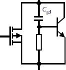
FIGURE 2.10 Parasitic bipolar transistor.
Their performance for representative Fuji devices in the 600 V class is next illustrated:
• Technology evolution with time (Figure 2.11)
• Evolution of the figure of merit “Ron * Qgd” over time (Figure 2.12) [3]
• Evolution of figure of merit “Ron * Area” over time (Figure 2.13) [3]
Since different technologies are more suitable for low voltage power switches (60 V) that mostly target automotive applications, the performance of products in this category is presented separately. This is presented for information only, as these devices are not directly used in medium and high-power converters (that is the topic of this book). Criteria for illustration of results are
• Technology evolution with time (Figure 2.14)
• Evolution of the figure of merit “Ron * Qgd” over time (Figure 2.15) [3]
• Evolution of figure of merit “Ron * Area” over time (Figure 2.16) [3]
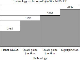
FIGURE 2.11 Technology evolution and years of product release.
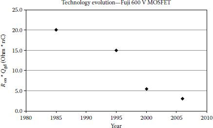
FIGURE 2.12 Evolution of the figure of merit “Ron * Qgd” over time.
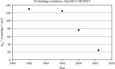
FIGURE 2.13 Evolution of figure of merit “Ron * Area” over time.
Design of gate drivers depends on the switching characteristics. The switching times given in datasheets as electrical characteristics are for resistive load switching. The performance curves are for half-bridge inductive load, as they are the most prevalent application of IGBTs.
Circuits used to control power MOSFET devices are called gate drivers. A MOSFET gate driver has the simple task of providing a voltage for the gate control, and it does not require a large amount of current. The gate current is large at the beginning and limited by the resistance at the gate circuit. Depending on the level of the gate threshold voltage, gate control is usually performed with voltages at logic level (5 V) or from complementary metal oxide semiconductor buffers (15–20 V). Many integrated gate driver circuits are available for both situations, along with protection circuits for fast shutdown (e.g., TPS2812).
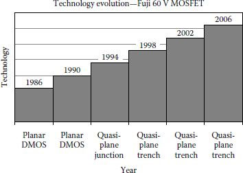
FIGURE 2.14 Technology evolution and years of product release.
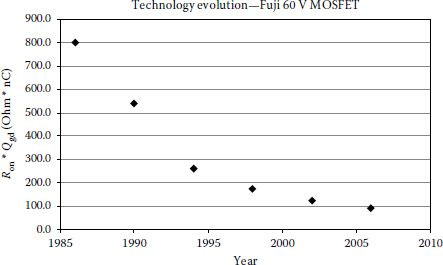
FIGURE 2.15 Evolution of the figure of merit “Ron * Qgd” over time.
Given the small amount of capacitance to be charged, MOSFET gate drivers should ensure a fast variation of the control voltage with slopes below 20 ns.
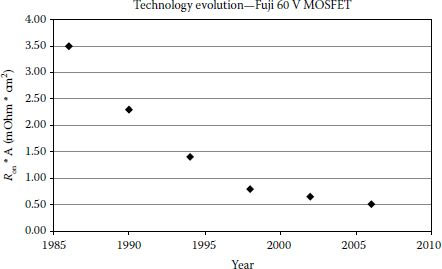
FIGURE 2.16 Evolution of figure of merit “Ron * Area” over time.
The gate-source voltage should not be higher than a datasheet parameter, VGS(max). This is determined by the requirement that the gate oxide not be broken down by a large electric field. Another consideration is the paralleling of MOSFETs, which is presented in Chapter 12.
2.3 INSULATED GATE BIPOLAR TRANSISTORS
IGBTs combine the advantages of bipolar transistors, such as low conduction losses, with the merits of MOSFETs, such as shorter switching times. For this reason, the switching behavior of IGBTs can be analyzed based on MOSFET models described earlier. The conduction interval is better modeled with the characteristics of a saturated bipolar transistor. Because of the smaller voltage drop at conduction, IGBT devices are used at higher voltages than the MOSFET devices (Figure 2.17).
Without entering into the details of the semiconductor structure, let us first focus on the IGBT model presented in Figure 2.18. It considers the IGBT formed as a Darlington combination of a main MOSFET device and a pnp transistor. Unlike the conventional Darlington, the MOSFET device carries most of the current. The parasitic npn transistor has the same origin and effect as the parasitic transistor from the MOSFET structure.
Switching characteristics of IGBT devices are highly similar to those of the MOSFET devices. The major difference consists in the bipolar effect at turn-off, when a tail current still persists for a certain amount of time. Because of this tail current, the IGBT devices are not very suitable for use within zero-voltage switching (ZVS) applications and generally introduce additional switching loss.
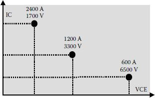
FIGURE 2.17 Present limits of the IGBT technology (example from EUPEC product line).
The tail current is also the source of an interesting design trade-off. This current exists due to the charge stored in the drift region. As the MOSFET section is OFF and there is no reverse voltage applied to the device to generate a negative drain current, there is no possibility of removing the stored charge. This can finally be removed by recombination within the IGBT. Here comes the trade-off. The excess carrier lifetime is required to be large for a small voltage drop in the conduction state. This would determine a slow recombination and a long existence of the tail current.
This is the most-used method to minimize the magnitude of the tail current, or the magnitude of the bipolar current within the IGBT device. The device is designed to have 90% or more drain current passing through the MOSFET structure and only a small amount of current through the bipolar transistor, which can be achieved with a low beta of the pnp transistor.
An alternative technological solution to this problem is the so-called punch-through (PT) technology. The PT IGBT minimizes current-tailing by shortening the duration of the tailing time, with one n+ layer acting like a sink for the excess holes. This buffer layer allows the drift region to be smaller than that of the non-punch through (NPT) IGBTs, resulting, consequently, in a reduced voltage drop in the conduction state.
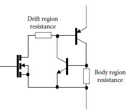
FIGURE 2.18 Equivalent model of an IGBT device.
The characteristics of both NPT IGBT and punch through (PT) IGBT have been improved over the years (F). Their technology development is marked by the following top characteristics:
PT IGBT:
• Improvements rely on the buffer layer structure and the carrier lifetime reduction processing.
• The major drawbacks are related to
• The extremely high-carrier concentration in the buffer layer causes undesired high turn-off current and hence increased losses.
• The processing to reduce carrier lifetime results in an increased forward voltage drop.
NPT IGBT:
• Improvements rely on geometry optimization allowing reduction of the wafer layer thickness.
• The major drawback relates to the thick n-drift region that leads to higher static and dynamic losses. This thick n-drift region is needed for voltage blocking.
The newer Field-Stop (FS) IGBT structures are overcoming the drawbacks of the two structures by vertically shrinking the NPT IGBT to a structure with a thin n-drift region, while inserting a low doped field-stop layer instead of the high doped buffer layer used in the PT IGBT (Figure 2.19). Therefore, the Field-Stop IGBT exhibits reduced overall losses and better high-voltage performance.
The weakly doped field-stop layer in the FS IGBT gives a trapezoidal electric field distribution under forward blocking (similar to the PT IGBTs), which is more desirable than the triangular electric field distribution of NPT IGBTs. This further provides a reduction of the drift region thickness for the same blocking voltage.
The advantages of the NPT IGBT devices (low-efficiency emitter and the high-carrier lifetime) are still maintained because the field-stop layer only pins the electric field under forward blocking without reducing the p-emitter injection efficiency, unlike the injection efficiency reduction from the highly doped buffer layer in the PT structure.
Variations of the Field-Stop IGBT technology are improving further these main properties (like the Advanced Field Stop trench IGBT, AFS-IGBT).
The actual performance of these three technologies (NPT IGBT, PT IGBT, and FS IGBT) can be briefly observed within the following figures, compiled from various sources featuring Fuji devices [4,5,6,7]. While different manufacturers report merits and demerits of their own technologies, sampling the product performance of a single manufacturer illustrates somewhat the state of the technology at a given time. Criteria illustrated in these figures are
• Technology timeline (Figure 2.20)
• Maximum current for each chip on the respective technology (Figure 2.21)
• Evolution of inverter loss over time (Figure 2.22)
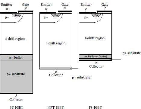
FIGURE 2.19 Principle of the three IGBT technologies.
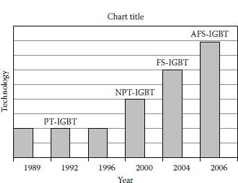
FIGURE 2.20 Approximate launching year for each technology.
• Chip area (size) over time (Figure 2.23)
• Semiconductor design rule over time (Figure 2.24)
Very similar results are reported in [8] for the technology evolution for IGBT devices made by Infineon and in [9] for IGBT devices made by Semikron. The performance of the FS IGBT technology is also investigated in [10,11].
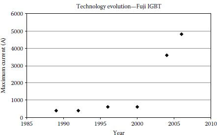
FIGURE 2.21 Maximum current achievable with each technology.
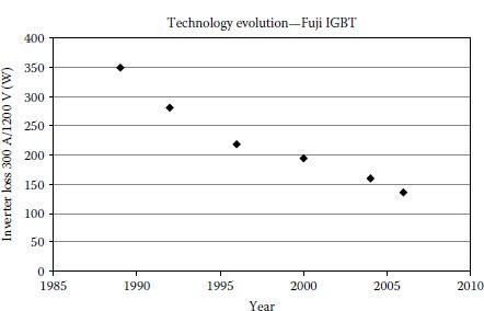
FIGURE 2.22 Evolution of inverter loss over time.
The latest generation of IGBT devices, after the emergence of FS IGBT, featured the trench gate. Trench gate technology developed in parallel with field-stop, and it was incorporated in both MOSFET and IGBT devices, independent of the application of the field-stop features. The advantages of trench gate devices consist of the use of a vertical channel that requires less area compared to the horizontal channel of planar structure. This provides a greater cell density, greater channel width/unit area, and a lower RDS(on). Moreover, there is no parasitic JFET between adjacent cells, and this also helps a greater cell density and lower RDS(on). The advantage of a smaller ON-resistance is even more prominent at lower voltage ratings, where the channel resistance represents a more important contribution to the ON-resistance.
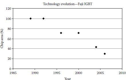
FIGURE 2.23 Evolution of chip area over time.
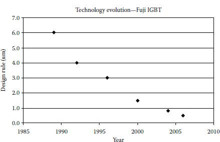
FIGURE 2.24 Evolution of semiconductor design rule over time.
The major requirements for the IGBT gate driver are highly similar to those of a MOSFET device. However, IGBT devices usually require a negative gate voltage for turning-off, with the exception of a class of IGBT devices designed for operation with unipolar voltage. Negative OFF-state control voltage and appropriate gate resistance can prevent cross-conduction. When the high-side IGBT turns on within an inverter leg, the voltage across the low-side IGBT increases with a high (dv/dt).
This induces a current in the gate of the IGBT that may produce turn-on of the low side device short of the DC bus. A negative gate voltage prevents this by providing a different path for the gate current. The same possible turn-on due to (dv/dt) can take place within a MOSFET as well, but the input capacitance is different and the chances of cross-conduction are minimal. This can be understood by looking at the ratio of reverse transfer capacitance to the input capacitance, which is larger for IGBTs (Cres/Cies). This produces an increased Miller effect, and a larger noise is coupled from collector to gate. However, certain low power IGBTs do not need negative gate voltage for turn-off, as their design minimizes Cres (reverse transfer). Another reason for the negative gate voltage at IGBTs is of the operation at higher voltages with increased (dv/dt) coupling of noise.
Figure 2.25 shows the minimal requirements of the gate driver circuit: a power supply able to ensure enough gate current, a gate-driving circuit, and a gate resistor. As the IGBT can float with respect to ground at the power stage, both the power supply and the gate circuitry should be isolated from the inverter ground. This gives room to a limited number of gate-driver configurations [12,13].
• Gate drivers with potential separation
• Gate driver with inductive transfer of power (power supply of up to 1 MHz intermediate frequency) and a direct information transfer
• Gate driver with inductive transfer of energy (power supply of up to 20 kHz intermediate frequency) and optocoupler transfer of information
• Gate drivers without potential separation
• Gate driver with bootstrap for power supply of high-side and level shifter for sending switching control information
In all these designs, a series resistor is employed at both turn-on and turn-off (Figure 2.25) that is usually implemented with a passive resistor. Advanced gate driver design requires different resistors for turn-on and turn-off. The value of the gate resistor within the range of values suggested by the IGBT/MOSFET manufacturer influences different aspects of the switching process. Figure 2.26 illustrates this graphically [14].
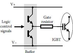
FIGURE 2.25 Gate driver concept.
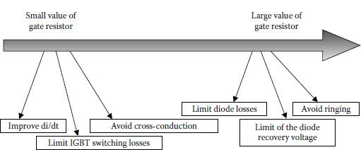
FIGURE 2.26 Effect of the gate resistor.
The gate current and the appropriate power of the voltage supply depend on the operating frequency, bias control voltages, and total gate charge. The total gate charge is published in IGBT/MOSFET datasheets, depending on gate-control voltage. The gate charge necessary for switching is very important to establish the switching performance of a MOSFET or IGBT. The lower the charge, the lower is the gate-drive current needed for a given switching time [15].
The average gate current can be calculated as is = Q ⋅ freq. The total gate power can be estimated as P = iS ⋅ (VG + − VG−). Therefore, the power requirements for the gate circuit are reduced to a small-power level and a high-peak gate current. This peak current can be roughly estimated as IG(Peak) = (VG + − VG−)/R.
2.3.2.2 Optimal Design of the Gate Resistor
As shown in Figure 2.26, the selection of the gate resistor influences performance of the converter. Considering an advanced gate driver with different gate resistors for turn-on and turn-off [16] allows us to perform an optimal selection of the gate resistor in order to control (dv/dt) and (di/dt) during switchings. The converter can thus be designed to operate snubberless [17,18].
Design constraints for optimization include:
• Minimum (dv/dt)on at highest current
• Maximum allowable peak voltage at turn-off
• Minimum (dv/dt)off for any current
• Avoiding cross-conduction through the (dv/dt)-induced current
The following calculations refer to Figure 2.25.
2.3.2.2.1 dv/dt at Turn-On
Let us observe Figure 2.3. Immediately after the turn-on signal has been applied, the VGE voltage rises from VGmin to VGE(th) due to the currents flowing through the input capacitances (Cge and Cgc). The rate of rise is almost linear across the equivalent input capacitance (as approximation of a part of an exponential curve with a time constant of τ1 = RGON * Cies).
After the gate voltage passes VGE(th), the collector current begins to increase with a rate given by the current/voltage characteristics:
(2.1) |
The current within the gate circuit can be described with the equation:
(2.2) |
where VGE(IL + IRM) represents the Miller voltage, and V+G is the positive gate supply voltage.
The voltage equation for the gate circuit should include the parasitic inductance that is composed of IGBT package inductance and external connection inductance. This value is usually provided in the device datasheet as LE.
(2.3) |
It yields:
(diCdt)on=V+G−VMiller(Cies⋅RGongfe)+LE=V+G−VGE(IL+IRM)(Cies⋅RGongfe)+LE |
(2.4) |
After the gate voltage reaches the Miller plateau, the entire gate current is flowing through the gate-collector capacitance, causing the collector voltage to drop at a rate of
(2.5) |
with the maximum value at IC = ILoad.
If we want to obtain a (dv/dt) higher (faster) than a specified minimum value, the gate resistor should be less than:
(2.6) |
2.3.2.2.2 dv/dt at Turn-Off
After the turn-off control signal has been applied, and the IGBT crosses the active region, the VGE is clamped to a constant value that is the voltage needed to maintain the IL load current.
(2.7) |
The entire gate current flows through Cgc and causes the voltage variation:
(dvGCdt)=dvCEdt=iGCgc=−V+G+VGE(IL)RGoff⋅Cgc=VGE(th)+12⋅ILgfe−V+GRGoff⋅Cgc |
(2.8) |
If we want to obtain a (dv/dt) higher (faster) than a specified minimum value, the gate resistor should be less than:
(2.9) |
2.3.2.2.3 Peak Voltage at Diode Turn-Off
The overvoltage across the inverter leg should be limited to a pre-established value (for instance 5%). This over-voltage occurs at any fast current variation (switching) in the inverter leg, and it is most important at diode turn-off when the recovery current is superimposed to the conventional switching of the load current. This occurs when IGBT turns on. The design value for the gate resistance yields from Equation 2.4:
(Cies⋅RGongfe)+LE=V+G−VGE(IL+IRM)(diCdt)⇒RGon≥RGon, min =gfeCies⋅[V+G−VGE(IL+IRM)(diCdt)reqon−LE] |
(2.10) |
This design equation can be expressed also directly from the peak voltage:
RGon≥RGon, min =gfeCies⋅[V+G−VGE(IL+IRM)|VDC−VPeak|2⋅Lst−LE] |
(2.11) |
where Lst is the stray inductance of the busbar connection between the inverter leg (IGBT) and the actual DC source (usually an electrolytic capacitor).
2.3.2.2.4 Avoiding Cross-Conduction
A fourth design constraint comes from the request to avoid cross-conduction due to the large (dv/dt). If we suddenly apply a large dv/dt across an IGBT device, currents may start to circulate within. The collector-gate current would become gate current and supply the IGBT turn-on through the actual gate resistor RGoff.
It yields
(2.12) |
(2.13) |
(2.14) |
The variation of the gate voltage can be considered as being zero (dvG/dt = 0) during the Miller plateau interval. This reduces at
(2.15) |
The peak of the induced gate voltage results as
(2.16) |
Equation 2.5 into 2.16 yields
(2.17) |
Appropriate value of the gate resistance can prevent this shoot-through conduction. When considering the “on” resistance defined by previous conditions, the “off” gate resistance can be calculated from this relationship for different gate voltage and load current values.
Automated design procedures can be implemented on computer software based on the above considerations as well as from considering parameter variations [18].
A power converter equipment includes a set of protection circuits and features. Chapter 6 presents in detail the practical aspects of building a power converter. Before such a design can be accomplished, the datasheet information about the limits of operation should be understood.
The proper operation of an IGBT or MOSFET device is bounded by datasheet limitations. The collector current is limited to avoid latch-up. The maximum gate emitter voltage is set by the gate oxide breakdown considerations. The maximum current that can flow under short-circuit with a maximum gate-emitter voltage is four to ten times the nominal rated collector current. The maximum collector–emitter voltage of an IGBT device is set with the breakdown voltage of the internal pnp transistor. The maximum junction temperature is 150°C.
Special datasheet information refers to the safe operating area (SOA). Both IGBT and MOSFET devices have square SOAs for short switching times. If the conduction intervals are longer, thermal aspects modify the SOA, as shown in Figure 2.27. Modern IGBT devices can operate at the corner of the SOA for 10 μs (Figure 2.27). This allows a protection circuit to trigger the gate signal and to protect the IGBT at high currents. In other words, the IGBT can operate in short-circuit for up to 10 μs [12].
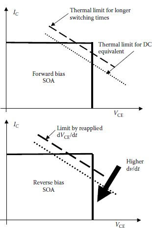
FIGURE 2.27 Ideal SOA and limitations due to special operation conditions.
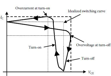
FIGURE 2.28 Switching characteristics.
The parasitic components of the collector–emitter circuit determine a real switching characteristic far from a square one. The designer should make sure that this real characteristic is always inside the SOA (Figure 2.28). These trajectories depend upon stray inductances, parasitic capacitances, and the MOSFET’s switching performance as (di/dt), (dv/dt). The IGBT package itself has a stray inductance of about 10–20 nH [12,19].
As the switching characteristics are the results of nonlinear phenomena, there are different methods to estimate the power loss. Power loss and efficiency of the power stage are very important, given the use of MOSFET and IGBT devices in power-conversion circuits.
There are two major methods for loss estimation:
• Calculation of energy loss based on analytical investigation of the switching waveforms
• Estimation of the energy loss based on empirical models derived from bench measurements
Observing the collector current and voltage waveforms, switching loss can be derived by calculating the areas of VI regions that correspond to the switchings.
The switching-loss energy at IGBT turn-on (Figure 2.3) is [17,18]:
ETon=0.5⋅[VDC−Lst⋅(didt)on]⋅(IL+IRM)2(didt)on+0.5⋅IL⋅V2DC(dvdt)on |
(2.18) |
where we assumed Lst as the stray inductance, VDC as the bus voltage, IRM as the peak recovery current of the adjacent diode, (di/dt) and (dv/dt) as the datasheet information about the selected semiconductor device.
The turn-off energy is calculated with (see Figure 2.5)
EToff=0.5⋅V2DC(dvdt)off⋅IL−0.5⋅[VDC−2⋅Lst⋅(didt)off].(IL)2(didt)off+0.5⋅kt⋅VDC⋅IL⋅ttail |
(2.19) |
The last term corresponds to the tail current at the IGBT turn-off and should miss at the same calculation performed for a MOSFET device. It can be seen that the gate drive circuit (especially the gate resistance) influences the switching losses by di/dt, dv/dt, IRM, and overvoltage.
Finally, the diode turn-off within an inverter leg is characterized by loss expressed by
(2.20) |
The conduction loss is calculated as
(2.21) |
Integral across the fundamental period T can be reduced to integrals across all conduction intervals during a period.
Total losses can be calculated by adding up the switching and conduction losses, by taking into account the inverter topology, the modulation function for each device, and the operation mode or load power factor.
The second approach to loss estimation is based on bench measurement of power losses under specified conditions, followed by interpolation of results from these measurements for the actual circuit operation.
An example for this procedure is provided in [20], where the power loss equations for a three-phase inverter power module are determined by experiment rather than analytical calculation. In this respect, it is first determined that the power loss depends on actual load current and steady-state measurements are made for each possible load current. Given the peculiar construction of the IPM module, an empirical calculation of the loss is preferred [20].
This empirical model considers each switch individually and calculates the power loss with the following set of equations (valid for IRAMS devices [20]):
(2.22) |
(2.23) |
(2.24) |
The results of this method used for a conventional motor drive application built with a 20 A IPM module show 2.3 W power loss per switch, and 14.1 W per entire package, when operated in ambient temperature and trying to prevent a junction temperature close to 125°C.
The role of a passive gate-driver resistor has already been explained. It has also been shown that the value of the gate resistor influences different characteristics of the switching circuit (Figure 2.26). These performance aspects are not based on simultaneous phenomena and introduce the possibility of an idealistic control through a variable gate resistor. A variable value of the gate resistor can be achieved with an active gate control [21,22,23,24,25,26,27,28,29,30].
Historically, the use of active gate control was first mentioned in series connection of IGBT devices. This is required in medium-voltage applications, when the DC bus has values in thousands of voltage range. Series connection of IGBTs raises the problem of unequal voltage-sharing across these devices. The unequal voltage sharing across the IGBTs is due to
• Different delay times in gate driver and power semiconductor device
• Small parameter deviation among different devices
• Different reverse recovery behavior of the free-wheeling diodes
• Increased (dv/dt) with the number of series-connected devices
Voltage-balancing between series-connected devices is traditionally achieved with individual snubbering of each IGBT device. To reduce the passive component count and volume, modern active-snubbering methods have been reported to limit (dv/dt) and the overvoltage (Figure 2.29).
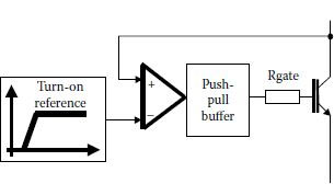
FIGURE 2.29 Active voltage balancing circuit used within series connected IGBTs.
Control of the collector voltage is achieved within an analog fast-feedback loop. Stability requirements imply design of a controller with poles at a frequency higher than gate circuitry, with a pole in the range of 1–10 MHz. Control bandwidth of 50–90 MHz is achieved with high-performance operational amplifiers. A significant loss reduction can be achieved by controlling the IGBT voltage in closed-loop operations only near the peak rating. Open-loop operation can be considered for the rest of the operation range. This obviously complicates the control circuit.
The downside of this solution can be seen at inductive loads. The IGBT voltage cannot respond to the gate voltage turn-on control until the free-wheeling diode has turned off. The closed-loop approach charges the gate quickly, producing a very high (di/dt).
Historically, the second step in active gate control was in short-circuit protection. If the collectors circuit experiences a short-circuit, the protection circuit tries to shut the gate down and cut the current. This produces a large (di/dt) and a large overshoot. The equivalent gate resistance increases when the protection acts to turn the IGBT off with a soft shutdown. This avoids the large (di/dt) and the large voltage overshoot.
Voltage-overshoot protection can be achieved by including an additional transistor stage in the gate driver (Figure 2.30) [31]. At turn-off, Qprot is turned on and the current is discharged through it. When the collector voltage reaches the breakdown voltage of the Zener diode, a current will flow through the gate of Qprot and will turn it off. The remaining current would flow through Rgate(off) slowing down the (dv/dt) rate.
Modern gate drivers adjust (di/dt) and/or (dv/dt) independently according to criteria, such as electron magnetic interference (EMI) emission control or efficiency improvement through snubberless operation. For instance, the gate resistor can be optimized to reduce EMI emission through controlled (di/dt) and/or (dv/dt). Usually, this value increases loss. These two constraints require different values of the gate resistors during operation.
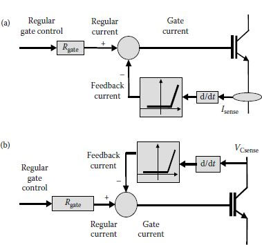
FIGURE 2.30 Principle circuits for active gate control: (a) based on (di/dt) optimization; (b) based on (dv/dt) optimization.
There are different methods for active control of (di/dt) and (dv/dt) (Figure 2.30). The simplest control is the feedback control of the gate current based on the device current or voltage slopes. Sensing the current or voltage slopes is carried out with a shunt resistor, on Kelvin emitter, on the information resulting from the Miller effect sensing.
The active gate control is not easy to implement. The circuit designer faces several constraints related to a fast event time scale that does not allow delays within the analog circuit and to a feedback dependence on IGBT parameters.
Consider the experiment shown in Figure 2.31 and the results in Figure 2.32 [21].
The gate voltage has an intermediate voltage level that decreases the gate current level on the first slope of turn-on. The voltage level ΔVs and the length of the time interval Δtts within this voltage level are adjusted. The IGBT/MOSFET behavior is a result of variable inductance. Despite the clear demonstration of the principle of active gate control, this experiment is not easy to implement. Generally, the strong nonlinear character and the detection of the Miller plateau are a problem.
Different solutions were reported in the literature for active gate control even from late 1900s [32,33,34,35,36,37,38,39,40,41,42]. Because all of the active gate drivers need a design dependent on the actual IGBT device to be controlled, these technologies did not make it into too many IC solutions. Several recent IPM products are taking advantage of dynamically controlled gate drivers only.
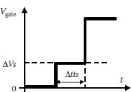
FIGURE 2.31 Principle of a simple experiment.
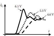
FIGURE 2.32 Results of the simple experiment.
2.6 GATE TURN-OFF THYRISTORS (GTOs)
As shown in the introduction to this chapter, gate turn-off thyristor (GTO) devices are used at high levels of current and voltage. They are a derivative of SCR devices, with a p–n–p–n structure, and can control both turn-on and turn-off processes. The operation is based on conventional recombination processes and the physics of junctions.
The major drawback of these devices is the large current required in the gate circuit for turn-off. Moreover, the GTO has a very low gain which means it requires a sophisticated and expensive gate drive. It is therefore impractical to use a charge extracting drive circuit, and so the GTO has a “tail effect” whereby the device still conducts while the minority carriers combine naturally.
Despite the technology saturation in what concerns conversion circuits and converters, the power semiconductor sector is still dynamic. There is continuous development along existing devices like MOSFET and IGBT. New generations of IGBTs and MOSFETs are introduced each year to the market and their performance is continuously improving, especially through the design rule improvement (the pitch resolution in defining the shape of each semiconductor region).
However, the most exciting news about completely new devices is their ability to change performance patterns through disruptive innovation. These disruptive devices can be classified in three categories:
• New devices solving certain issues with conventional devices and hence dedicated to certain peculiar applications (IGCT, IGBT-RC, IGBT-RB, and so on).
• High-frequency, high-voltage devices aiming at increasing the operation frequency with a degree of magnitude, and therefore requiring a complete overhaul of the inverter assembly.
• Devices using emerging new substrate materials and aiming at efficiency improvements through a new class of devices. Their novelty may lead to changes in the design of the gate driver and/or protection circuitry and hence may not be useable as a drop-in substitute for the existing components.
A good example of device especially designed for medium and high-power applications is the integrated gate commutated thyristor (IGCT). Its architecture is combining the best features of an IGBT and a GTO. The new solid-state switch is for medium-voltage applications from 2 to 6.9 kV, with maximum ratings of 4000 A, which builds upon the drawbacks of IGBTs that have high conduction losses and GTOs that are slow and require additional circuitry.
Through this new architecture, the IGCT makes possible designs that have not been feasible in the past. Thus, engineers need not design around IGBT and GTO trade-offs, which often impose limits on starting torque and regeneration ability of motor drives.
The Reverse Conducting IGBT is a very new device proposed to the market by Infineon at the end of 2009 [43]. This new device addresses the motor drives market, and it is especially successful within the BLDC motor drives controlled with the 120° program. Other applications include the soft-switching converters used within the induction heating and induction cooking products. This device incorporates the diode monolithically along the IGBT, providing low conduction losses of both IGBT and the integrated diode. This helps reducing the overall losses.
The increasing use of power electronic converters in energy processing has brought into attention topologies like Current Source Inverter, Matrix Converter, or the Neutral Point Clamped Inverter that require AC switches. All of these topologies promise a better power density for a given application. The conventional solution for preventing reverse conduction consists in connecting a diode in series with the usual IGBT. This is increasing the voltage drop during conduction state.
An alternative solution was proposed in early 2000 s with the IGBT-RB device. This device has the capacity to block voltage of both polarities without adding any supplemental series diode. Figure 2.33 is based on data compiled from [44,45], and it shows the improvement of the trade-off between the turn-off energy and the voltage drop during the conduction state.
The dependency shown in Figure 2.33 is used for comparing different power semiconductor technologies. Each curve is typical for a certain technology, and different products are at certain points of the technology performance curve. For instance, an IGBT for motor drives can aim at a low voltage drop in the conduction state as it is switched at low switching frequencies and the efficiency can be improved with reducing the voltage drop. Such a device would sit in the top-left corner of the technology curve. By contrary a different IGBT product made with the same technology can be aimed at use within UPS and power supplies applications where switching at a high switching frequency would reduce the filter requirements. Such an IGBT device would sit in the bottom-right corner of the technology curve. Figure 2.34 illustrates further this figure of merit by showing Powerex devices and their technologies [46]. To avoid a direct comparison between products of different manufacturers (which is not the goal here), Powerex products and technologies of the year 1999 have been compared in Figure 2.34, and Fuji products and technologies for the year 2010 are shown in Figure 2.33. Both figures are given for illustration of this performance figure of merit.
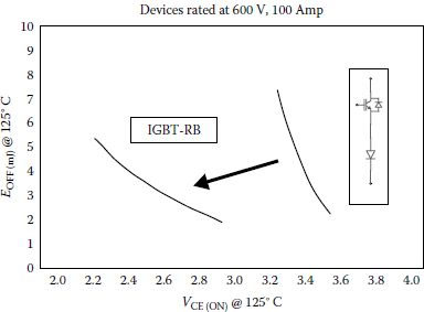
FIGURE 2.33 Performance improvement with the use of an IGBT-RB device instead of a conventional IGBT-Diode pair.
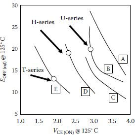
FIGURE 2.34 Evaluation of different Powerex IGBT technologies: A = conventional NPT, tN = 250 mm, Jc = 100 A/cm2; B = PT planar gate uniform lifetime control, Jc = 100 A/cm2; C = thin drift region NPT, tN = 150 mm, Jc = 100 A/cm2; D = PT planar gate, uniform lifetime control, Jc = 75 A/cm2; E = PT trench gate, local lifetime control, Jc = 140 A/cm2.
2.7.2 HIGH-FREQUENCY, HIGH-VOLTAGE DEVICES
Another power semiconductor device that is picking up in the market is the CoolMOS, a MOSFET with a special structure, rated up to 600 V, and able to switch up to 50 A. These devices change the entire way we think about power converters.
Design of the power stage is limited by the parasitic of the implementation (printed circuit or busbar). The idea of switching, say, a 400 V bus at 250 kHz, pushes the designer to be very careful while designing circuit details.
Given the requirements of a general overhaul of the power electronics equipment, the penetration of these devices as a substitute for conventional IGBTs was not very spectacular. They remain attractive solutions for high-power density equipment like certain aviation systems.
2.7.3 USING NEW SUBSTRATE MATERIALS (SiC, GaN, AND SO ON)
A generic trend in emerging power semiconductor devices is the use of new substrate semiconductors [47].
The development of new device technology started from within academic laboratories and small-business companies, and hence their experimental character has recommended them onto lower power converter market. The first applications included industrial applications in the HEV automotive market, IT and consumer, grid connected low power converters, or certain appliances. According to [44], the most dynamic sector is represented by the power factor correction converters in sub-kW power range. The SiC device technology being a little more advanced was able to bring up devices for applications up to MW power range. The GaN technology started 10 years after the SiC technology, and is currently featuring mostly diodes.
The success of the new substrate material semiconductors is mostly seen in diodes replacing conventional recovery diodes. The first application was the power factor correction circuitry in early 2001. The use of SiC diodes in the PFC application leads to power conversion improvement of around 2.4% [47] and a more optimal packaging. The losses are reduced tremendously and there is virtually no cost of circuit adaptation. Moreover, different auxiliary components like small inductor snubbers can be removed from circuit. The remaining obstacle is yet the slight cost difference (to beat the $0.20/Amp barrier).
Another good example is the recent release of IGBT-Diode copack devices built of standard Si-based IGBT and emerging SiC diodes, and dedicated to motor drives as a drop-in replacement or for new designs.
Conversely, the application of the power semiconductor switch made on new substrate material is more limited. The new devices are also requiring special gate drivers for control and protection and this is complicating the replacement in existing designs. Another limitation is the lack of reliability information or qualifications that prohibit somehow the use of these devices in applications with a critical lifetime or ruggedness requirements.
The new substrate materials devices do not present a major improvement for medium voltage converters switched at low switching frequency. The operation of high voltage (multi kV-range) converters will benefit from these new devices. Especially here, the plasma science or physics instrumentation equipment with operation at 50–100 kV would see major improvement with the use of SiC diodes for a considerable voltage drop across the device.
What concerns the high switching frequency application, here the voltage level matters again. At very low voltage levels, the soft-switching operation can easily be achieved with resonant converters and the merits of the new substrate material devices fade. At medium voltage (100s V) the new devices have clear merits over the use of conventional semiconductors at high switching frequencies.
The major advantages of using a complete SiC based technology instead of conventional Si devices can be briefly stated as [48]
• Approximately half of the chip area is required for a SiC JFET in order to achieve the same efficiency as with a Si MOSFET.
• When operating SiC devices with a junction temperature limit above 165°C, the heat-sink temperature can be higher and the size of the cooling system decreases.
• Hence, the power density increases.
• The same power density could be achieved if the SiC devices have 30–40% of the Si MOSFET chip area.
Successful design of power converters depends strongly on the information provided by the power semiconductor manufacturer within the datasheet. Each power device or class of devices is characterized with a peculiar technical document called “datasheet.” Let us see here how the information from a device datasheet has been gathered and what does it mean.
The first section of a datasheet includes a brief description of the device and a drawing of the device. In most cases, the application field is also suggested herein.
Even if presented in other random order, a first important section contains information about the absolute maximum electrical ratings of the device. If the operation of the power semiconductor device exceeds these ratings even on transients—it voids the manufacturer’s guarantee regardless of the duration or the conditions of the stress. Usually manufacturers use a test tolerance for these ratings when testing to establish the highest absolute-maximum rating. However, the circuit designer should never count on this tolerance band as it may vary from manufacturer to manufacturer. Alternatively, protective components can be used to completely alleviate operation beyond the absolute maximum ratings.
Any datasheet also provides three absolute maximum temperature ratings:
• Operating temperature is the maximum temperature over which you can operate the power device, even if there is no guarantee implied that electrical performance will be maintained over the entire operating temperature range.
• Junction temperature is the maximum temperature that the internal semiconductor die can reach under any environmental or operation condition.
• Storage temperature is the maximum temperature that the device may reach under a storage condition. This also voids the warranty offered by manufacturer for the device.
There is also another environmental warning regarding the ESD protection.
The most challenging information for a converter designer comes from the electrical characteristics tables. Each performance characteristics is reported along with test conditions for measurement, and it is provided with three fields: MIN (minimum), TYP (typical), and MAX (maximum). The manufacturer is trying to select the most significant test points. However, the circuit designer should exercise care in understanding the differences between the circuit under design and what the manufacturer is offering as test data. After initial assessment of their own power semiconductor devices, the manufacturer applies statistics to the data to obtain the mean value for each parameter. The following production batches are tested by statistical sampling for this datasheet information. The statistics yield the variance and sigma for the results distribution. The maximum and minimum values for each characteristics are selected at six times the value of sigma. These six sigma points become the minimum and maximum values for that parameter, and the mean is usually taken as the typical specification. Modern Design for Reliability concerns require the circuit designers to consider both the MAX and MIN values in order to cover all possible mishaps during operation rather than reducing the design to the use of TYP values. Alternatively, the designer may use its own statistical process of evaluation for the in-circuit tests of the new design.
A section of the datasheet contains graphs and table data for parameters that may vary with different operation points.
This applications related section often includes parameter measurement information, or unusual measurement circuits. The application section covers load-driving capability, layout and heat-sink suggestions, safe-operating area curves, special stabilization techniques for control circuits if included, or Spice models. All this information is provided by application engineer with experience in product and with a desire to present the product at its best. Such examples are eye-catching and not necessarily the best solutions for very large volume production. This is why the modern Design for Reliability concerns should be applied in all phases of design.
P2.1 |
Try to explain the variation of the gate-drain and gate-source capacitances? |
P2.2 |
The on-resistance of a power MOSFET equals 120 mOhms at a junction temperature of 25°C and increases linearly with temperature up to 200 mOhms at 100°C. Calculate the conduction loss in function of the operation temperature if the load resistance is 10 Ohms and the supply voltage is 150 V for a chopper operation. |
P2.3 |
Imagine a hybrid power switch made up of a bipolar transistor and a power MOSFET connected in parallel. What would be the benefits of such a device? |
P2.4 |
Qualitatively sketch the collector current versus time during turn-off for a short lifetime IGBT and for a long lifetime IGBT and explain the differences. |
P2.5 |
Qualitatively sketch the collector current change during the turn-on of an IGBT device controlled through different gate resistors. |
P2.6 |
Qualitatively sketch the collector current change during the turn-off of an IGBT device controlled through different gate resistors. |
P2.7 |
Write a computer program for power loss estimation based on the equations shown in this chapter and run this program for a simple case of a single IGBT switching a load resistor of 20 Ohms, at 20 kHz, from a DC bus of 400 Vdc. Consider a real IGBT device along with the manufacturer datasheet and compare results with those given in datasheet. |
P2.8 |
Consider a MOSFET and an IGBT with the same breakdown voltage and the same current rating. How would you compare the gate-drain and gate-source capacitances of these two devices? |
1. Anon. 2012. About the World Power Semiconductor Discretes and Modules Report, 2012 edition, IMS Research, July.
2. Anon. 2008. Power Semiconductors Market: Latest Trends 2008, Yano research.
3. Brown, J. and Moxey, G. 2003. Power MOSFET Basics: Understanding MOSFET Characteristics Associated With The Figure of Merit, Vishay-Siliconix Application Note AN-605, September.
4. Seki, Y. 2001. Present status and trends of power semiconductor devices. Fuji Electr. Rev. 47(2), 34–36.
5. Seki, Y., Hosen, T., and Yamazoe, M. 2010. The current status and future outlook for power semiconductors. Fuji Electr. Rev. 56(2), 47–50.
6. Fujihira, T., Kaneda, H., and Kuneta, S. 2006. Fuji’ electric semiconductor: Current status and future outlook. Fuji Electr. Rev. 52(2), 42–47.
7. Yamamoto, T., Yoshiwatari, S., and Ichikawa, H. 2012. Expanded lineup of high-power 6th generation IGBT module families. Fuji Electr. Rev. 58(2), 60–64.
8. Gutsmann, B., Kanschat, P., Münzer, M., Pfaffenlehner M., and Laska, T. 2003. Repetitive Short-Circuit Behavior of Trench/FieldStop IGBTs, PCIM Europe 2003.
9. Schreiber, D. 2005. New power semiconductor technology for renewable energy sources application, Semikron Seminar in Sevilla, Spain, Internet documentation.
10. Kang, X., Caiafa, A., Santi, E., Hudgins, J.L., and Palmer, P.R. 2003. Characterization and modeling of high-voltage field-stop IGBTs. IEEE Trans. Indust. Appl. 39(4), 922–929.
11. Dodge, J. 2004. IGBT Technical Overview, Application Note APT0408, Advanced Power Technology Corporation, November.
12. Anon. 1998. Using IGBT Modules, Mitsubishi Electric, September.
13. Motto, E. 1996. Gate drive techniques for large IGBT modules, PCIM Magazine.
14. Zverev, I., Konrad, S., Voelker, H., Petzoldt, J., and Klotz, F. 1997. Influence of the gate drive technique on the conducted EMI behaviors of a power converter. IEEE PESC 2, 1522–1528.
15. Hefner, A.R. 1991. An investigation of the drive circuit requirement for the power insulated gate bipolar transistor. IEEE Trans. Power Electron. 4, 208–218.
16. Neacsu, D., Takahashi, T., and Nguyen, H.H. 2000. Using IR 2137, International Rectifier Design Tip 00-1.
17. Blaabjerg, F. and Pedersen, K. 1997. Optimized design of a complete three-phase PWM-VS inverter. IEEE Trans. Power Electron. 12(3), 567–577.
18. Neacsu, D.O. and Takahashi, T. 2000. Computer-aided design of a low-cost low-power snubberless three-phase inverter, IEEE Workshop on Computers in Power Electronics, Blacksburg, VA, June, pp. 204–210.
19. Neacsu, D., Takahashi, T., and Nguyen, H.H. 2000. Using IR 2137, IR Design Tip 00-1.
20. Wood, P., Battello, M., Keskar, N., and Guerra, A. IPM Application Overview—Integrated Power Module for Appliance Motor Drives, International Rectifier AN-1044.
21. McNeil, N., Sheng, K., Williams, B.W., and Finley, S.J. 1998. Assessment of OFF-state negative gate voltage for IGBTs. IEEE Trans. Power Electron. 13, 436–440.
22. Ferrieux, J.P., Forest, F., and Lienart, P. 1989. The insulated gate bipolar transistor: switching mode, EPE Conference, Aachen, pp. 171–175.
23. Gerster, C.H. and Hofer-Noser, P. 1996. Gate controlled dv/dt and di/dt—Limitation in high power IGBT converters. EPE J. 5(3/4), 11–16.
24. Musumeci, S., Raciti, A., Testa, A., Galluzo, A., and Melito, M. 1997. Switching behavior improvement of insulated gate-controlled devices. IEEE Trans. Power Electron. 12(4), 645–653.
25. Takizawa, S., Igarashi, S., and Kuroki, K. 1998. A New di/dt control gate drive circuit for IGBTs to reduce EMI noise and switching losses. IEEE Power Electronics Specialists Conference, Fukuoka, Japan, vol. 2, pp. 1443–1449, July.
26. Lee, H.G., Lee. Y.H., Suh, B.S., and Hyun, D.S. 1997. An improved gate control scheme for snubberless operation of high power IGBTs, IEEE Industry Applications, Annual Meeting, New Orleans, Louisiana, USA, vol. 2, pp. 975–982, 5–9 October.
27. Hong, S. and Lee, Y.G. 1999. Active gate-control strategy of series connected IGBTs for high power PWM inverter, IEEE PEDS, Hong Kong, vol. 2, pp. 646–452, 27–29, July.
28. Gerster, C., Hofer, P., and Karrer, N. 1996. Gate-control strategies for snubberless operation of series connected IGBTs. IEEE PESC Conference, Baveno, Italy, vol. 2, pp. 1739–1742, 23–27 June.
29. Idir, N., Franchaud, J.J., and Bausiere, R. 2000. New control technique achieves low di/dt and dv/dt. PCIM Magazine, February.
30. John, V., Suh, B.S., and Lipo, T.A. 1999. High performance active gate drive for high power IGBTs. IEEE Trans. Indust. Appl. 35(5), 1108–1117.
31. Heath, D. and Wood, P. 1999. Overshoot voltage reduction using IGBT modules with special drivers. International Rectifier Design Tip no. 99-1.
32. McNeil, N., Sheng, K., Williams, B.W., and Finley, S.J. 1998. Assessment of OFF-state negative gate voltage for IGBTs. IEEE Trans. Power Electron. 13, 436–440.
33. Ferrieux, J.P., Forest, F., and Lienart, P. 1989. The Insulated Gate Bipolar Transistor: Switching Mode, EPE Conference, Aachen, pp. 171–175.
34. Gerster, C.H. and Hofer-Noser, P. 1996. Gate controlled dv/dt and di/dt—Limitation in high power IGBT converters. EPE J., 5(3/4), 11–16.
35. Musumeci, S., Raciti, A., Testa, A., Galluzo, A., and Melito, M. 1997. Switching behavior improvement of insulated gate-controlled devices. IEEE Trans. Power Electron. 12(4), 645–653.
36. Takizawa, S., Igarashi, S., and Kuroki, K. 1998. A New di/dt control gate drive circuit for IGBTs to reduce EMI noise and switching losses. IEEE Power Electronics Specialists Conference, Fukuoka, Japan, vol. 2, pp. 1443–1449, July.
37. Lee, H.G., Lee, Y.H., Suh, B.S., and Hyun, D.S. 1997. An improved gate control scheme for snubberless operation of high power IGBTs, IEEE Industry Applications, Annual Meeting, New Orleans, Louisiana, USA, vol. 2, pp. 975–982, 5–9 October.
38. Hong, S. and Lee, Y.G. 1999. Active gate-control strategy of series connected IGBTs for high power PWM inverter, IEEE PEDS, Hong Kong, vol. 2, pp. 646–452, 27–29, July.
39. Gerster, C., Hofer, P., and Karrer, N. 1996. Gate-control strategies for snubberless operation of series connected IGBTs. IEEE PESC Conference, Baveno, Italy, vol. 2, pp. 1739–1742, 23–27 June.
40. Idir, N., Franchaud J.J., and Bausiere, R. 2000. New control technique achieves low di/dt and dv/dt. PCIM Magazine, February.
41. John, V., Suh, B.S., and Lipo, T.A. 1999. High performance active gate drive for high power IGBTs. IEEE Trans. Indust. Appl. 35(5), 108–1117.
42. Luniewski, P., Jansen, U., and Hornkamp, M. 2005. Dynamic voltage rise control, the most efficient way to control turn-off switching behaviour of IGBT transistors, pelincec Conference, October 16–19, 2005, Warsaw, Poland, pp. 80.1–80.6.
43. Rebec, M. 2012. “RC-D Fast”: RC-Drives IGBT optimized for high switching frequency, Infineon Application Note, July.
44. Hosen, T. and Yanagisawa, K. 2011. Fuji electric’s semiconductors: Current status and future outlook. Fuji Electr. Rev. 57(3), 68–71.
45. Komatsu, K., Harada, T., and Nakazawa, H. 2011. IGBT module for advanced NPC topology. Fuji Electr. Rev. 57(3), 72–76.
46. Motto, E.R., Donlon, J.F., Takahashi, H., Tabata, M., and Iwamoto, H. 1999. Characteristics of a 1200 V PT IGBT with trench gate and local life time control, IEEE IAS Annual Meeting, pp. 811–816 vol. 2.
47. Anon. 2009. SiC and GaNi Power Electronics: Focus on PFC Market, Yole Development Report.
48. Schweizer, M., Waffler, S., and Kolar, J.W. 2011. SiC versus Si—Evaluation of potentials for performance improvement of inverter and DC–DC converter systems by SiC power semiconductors. IEEE Trans. Indust. Electron. 58(7), 2872–2882.