
Most of the other Chapters of the book dealt with the Voltage Source Converter, a power converter structure built of 6 bi-directional switches and supplied from a voltage source. An alternative topology consists of a Current Source Converter [1,2,3] (Figure 15.1). Such converter structure is built of 6 unidirectional switches and it is supplied from a current source. This means the converter must always ensure a current circulation and a path for this current. Furthermore, the current circulation is unidirectional from the DC current source to the load (for a Current Source Inverter), or from the AC grid to the DC current load (for an AC/DC Current Source Converter). The possible states are shown in Figure 15.2.
The oldest form of a Current Source Converter was the AC/DC SCR-Based Rectifier without the DC-side capacitive filter, where thyristors are controlled to adjust the load current that is flowing from grid to the load. The advent of IGBT devices shifted the focus more and more on voltage source type topologies since the current source topologies required additional blocking diodes to transform the IGBT-diode copack into a true unidirectional device. The recent appearance of IGBT-RB (reverse blocking) devices encourages a new look into the Current Source Converter topologies.
The DC/AC Current Source topology is mostly used for motor control and these motors are three-phase. Hence, only the three-phase converters will be analyzed in this chapter.
The advantages of the Current Source Converter/Inverter when compared to the counterpart Voltage Source structure are:
• Operation with reduced power loss [4,5].
• Operation with reduced noise.
• The lack of free-wheeling diodes improves the size and weight of the converter.
• The reliability yields improved due to less count of components.
The disadvantages of the Current Source Converter topologies are:
• Slower transient response of the current (considering the topology of converter + filter).
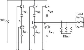
FIGURE 15.1 Three-phase current source inverter.
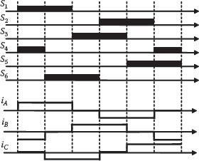
FIGURE 15.2 Switching states and currents for the un-modulated current source converter.
The sampling/switching frequency is usually chosen within the range 1–10 kHz in order to reduce the reactive energy generated in the AC-side leakage reactance during commutation and hence the devices’ stress. Other contemporary concerns refer to mitigation of the common-mode voltage [6].
The current control is achieved with an appropriate PWM algorithm able to adjust the current level through the modulation index m. Most of the PWM algorithms are similar to those for the Voltage Source Converters in terms of generating pulses by a comparison between a reference waveform and a carrier. Usually the reference waveform is trapezoidal [10,11] or sinusoidal [7].
The control of the power stage needs to ensure the conduction of only two devices at any moment. The transition between the different conduction states needs to be done seamless, without loss of current circulation. This is achieved with a mechanism similar yet opposite to the dead-time generator: a small interval is introduced to superimpose the two adjacent states by allowing conduction of switches defining both the old state and the new state. This concept is true for any PWM algorithm and for either AC/DC or DC/AC conversion.
For instance, at the state change from conduction of Sw1 and Sw6 to the conduction of Sw3 and Sw6, a circulation path should be maintained for the current entering the converter on the DC+ conductor (see Figure 15.2). Usually this is ensured with an interval when both Sw1 and Sw3 are controlled to be ON (Figure 15.3) [8]. This interval is called overlap and it must be long enough to turn ON the OFF switch before turning OFF the conducting switch. This overlap also provides a minimum ON time for the switches.
The actual current commutation between switches Sw1 and Sw3 depends on the polarity of the line voltage vAB (Figure 15.1). Both switches have gate signals for the conduction state and the polarity of the voltage drop across them dictates the conduction state. The exact commutation moment occurs either at the beginning or at the end of the overlap interval. This ambiguity in the exact commutation moment implies a loss of control and an uncertainty in the switch current, and further on the output line current during the overlap periods. Considering both edges of each PWM pulse of the AC-side current denotes three cases (similar to the analysis of effects of the dead-time interval):
• Pulse is shifted.
• Pulse is losing some current.
• Pulse is increased with certain length.
The overall effect of this change in the pulses’ shape yields in a slight distortion of the AC-side sinusoidal current waveform [9]. The waveforms are influenced as shown in Figure 15.4. Using fast switching devices allows operation with a short overlap time that will not distort or otherwise influence the current waveform.
Finally, it is important to note that the gate control cannot be achieved with conventional dual-channel (converter leg) or six-channel (inverter) gate drivers since these have the shoot-through protection implemented. Individual gate drivers would allow the conduction of both switches on the same inverter leg.
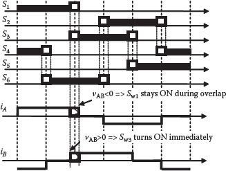
FIGURE 15.3 Control for current commutation.
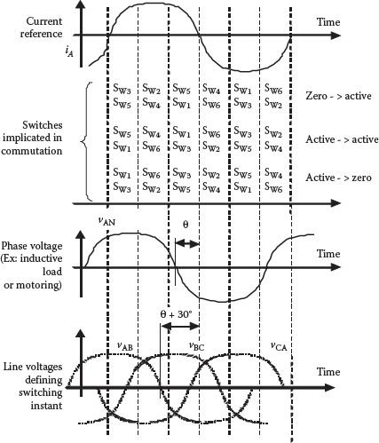
FIGURE 15.4 Influence of the overlap on the switching states.
15.3 USING SWITCHING FUNCTIONS TO DEFINE OPERATION
We have used switching functions to characterize the operation of a three-phase voltage source converter in Chapter 3, Section 3.8. The same theory is used herein for the Current Source Converter. Switching Functions are defined as periodical signals able to characterize analytically the change of states without entering the details of transitions between states. Let us consider the switching functions as being identical with the signals used for control of switches from Figure 15.1.
(15.1) |
(15.2) |
(15.3) |
The DC-side voltage can be computed from instantaneous output voltages as:
(15.4) |
These will further be used for modeling of the power converter when simulated in MATLAB-SIMULINK or PSPICE, and also for development of the PWM algorithm.
System level waveforms are shown in the following figures for a generic PWM algorithm without any compensation for overlap time or canceling of the possible filter resonance. Different improved options for the generation of the gate control pulses will be shown in detail within Section 15.4. These waveforms are shown herein for illustration of purposes at different switching frequencies. It can be seen how important is the selection of the filter components and the avoidance of possible oscillations within the filter structure (Figures 15.5, 15.6, 15.7, 15.8).
The AC/DC Current Source Converter (also known as Switched-Mode Rectifier) is represented in Figure 15.9. This time the PWM pulses are synchronized with the grid with a PLL-type circuitry. The same switching functions theory is employed for modeling of the operation.
The operation is very similar to the Current Source Inverter, but the energy flows now from the grid to the DC-side load. The proper operation is secured by the presence of an input L-C filter, where the inductance L makes up for the grid inductance and a possibly small added filter inductance. The switching functions are the same with Equations 15.1, 15.2, 15.3, 15.4.
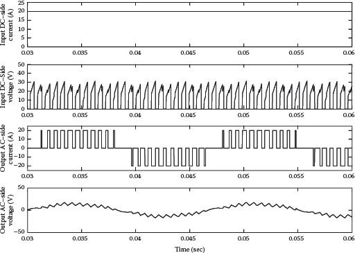
FIGURE 15.5 System-level waveforms for the current source inverter (fPWM/fout = 24, L = 1 mH, C = 470 μF).
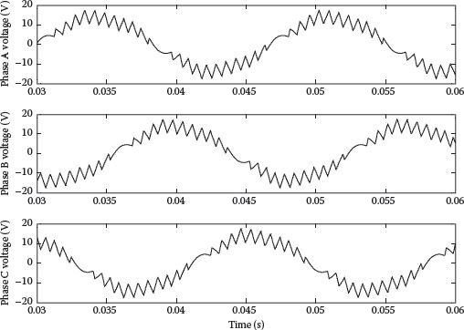
FIGURE 15.6 Output phase voltages after L-C filter (fPWM/fout = 24, L = 1 mH, C = 470 μF).
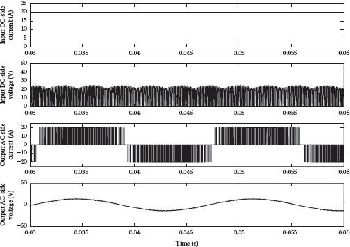
FIGURE 15.7 System-level waveforms for the current source inverter (fPWM/fout = 120, L = 1 mH, C = 470 μF).
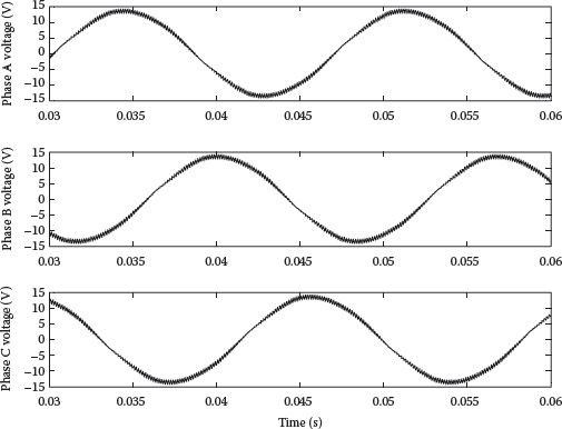
FIGURE 15.8 Output phase voltages after L-C filter (fPWM/fout = 120, L = 1 mH, C = 470 μF).
Simulation results are shown within the following figures. They are given for illustration purposes as the L-C filter components and the PWM control could be optimized further. It is important to mention the role of accurate synchronization between control and grid phase information (Figures 15.10 and 15.11).
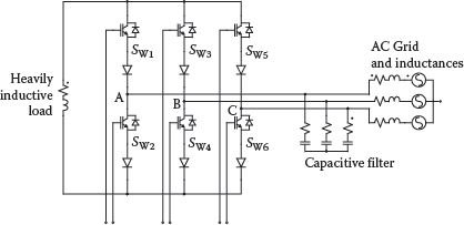
FIGURE 15.9 Switched mode PWM rectifier.
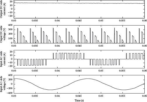
FIGURE 15.10 System-level waveforms for the grid-connected current source converter (fPWM/fout = 24, L = 2 mH, C = 470 μF).
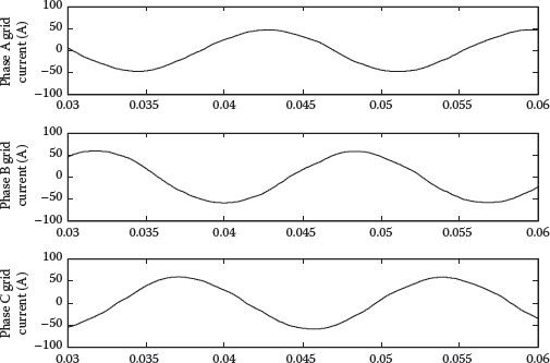
FIGURE 15.11 Grid currents (fPWM/fout = 24, L = 2 mH, C = 470 μF).
The operation described within Figure 15.2 and Equations 15.1, 15.2, 15.3, 15.4 cannot allow the adjustment of the current in the circuit. This is achieved further with various PWM control algorithms. Moreover, optimization within these PWM algorithms is also discussed.
The biggest difference between the PWM algorithms for the CSI and VSI structures consists of operation of only two switches at any given moment within CSI instead of three for the VSI. The two conducting switches belong to two different legs of the inverter and current flows in two phases only. In certain situations the two switches on the same leg are conducting, creating a short-circuit path able to circulate the DC-side current without stressing the AC-side filter capacitors.
The simplest PWM algorithm is following the principles of the carrier-based modulators for Voltage Source Converters (Figure 15.12). The reference signal is a trapezoidal waveform with unity magnitude, and the PWM pulses are produced by comparison during the slopes of the reference waveform. This method is called upon as Trapezoidal PWM [10,11]. The middle segment of the waveform is flat for 60°. Similar waveforms are used for the other two phases.
Figure 15.13 shows an example of the phase currents derived after the AC filter when using such a PWM method, when the PWM has a low ratio between the pulse frequency (switching frequency) and the fundamental (reference) waveform’s frequency.
15.4.2 HARMONIC ELIMINATION PROGRAMMED MODULATION
Observing the waveforms of Figure 15.12 suggests the PWM generation based on optimal algorithms like those described in Chapter 3, Section 3.7.1. Actually the mathematical results reported there can also be used for control of the Current Source Inverter when elimination of certain harmonics is imposed as design requirement. After the angular coordinates for the switching instants are determined by calculus, the actual PWM sequence will be determined respecting the control logic for a CSI converter.
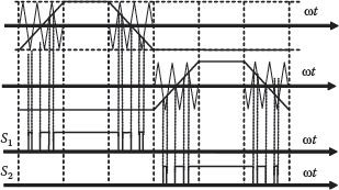
FIGURE 15.12 Carrier-based PWM method.
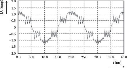
FIGURE 15.13 Example of phase current after the L-C filter, for a low frequency ratio.
It is worthwhile to mention that any PWM control algorithm for a three-phase voltage source converter can be used for control of a current source type structure when the difference between two control signals on different phases (like a line-to-line signal) is used for control of a single switch from the CSI structure. This is also apparent from comparison of the line-to-line voltage of a VSI converter that has the same shape with a phase current from the CSI operation.
Mathematical details and examples for this method are not repeated herein as they stand true from the previous explanation given in Chapter 3, Section 3.7.1.
Another PWM controller for the Current Source Inverter/Converter can be defined starting from a Sinusoidal reference like in the case of a controller for a Voltage Source Converter (Figure 15.14) [12]. First the signals pertaining to the converter states for the Current Source Converter are calculated with simple logic operators (Figure 15.15). This guarantees the generation of the 6 active states. Next the zero states derived by control of Figure 15.14 need to be identified as a safety measure. During such intervals, ON states need to be inserted in order to maintain the circulation of the current. Various logic circuitry can ensure this.
This logic is unfortunately not enough as it is necessary to also be able to generate the zero states and to select the proper sequence of switches. This can be carried out with a combinatorial logic as shown in [15].
A different approach more closely related to microcontroller implementation works with the converter state coded as a switching state. The conventional PWM controller calculates first the time intervals to be spent in different switching states. Then, the actual states are identified and coded. Based on the switching state code, the actual switch is selected with a memory table (Figure 15.16). The memory lookup table is shown as a “multiplexer + combinatorial logic” module in the simulation file, which actually can be another way to implementation. The fourth input to this table secures the generation of the zero state by continuation of the switch state. The gate control signals are shown in Figure 15.17.
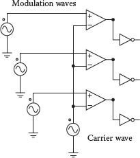
FIGURE 15.14 PWM generator for a voltage source inverter.
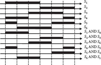
FIGURE 15.15 Determine the control signals from a conventional PWM generator for a VSI.
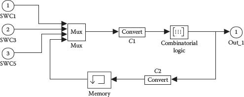
FIGURE 15.16 Selection of the switching state with a memory look-up table, as depicted from a conventional MATLAB-SIMULINK simulation file.
FIGURE 15.17 Control signals for the logic circuitry shown in Figure 15.16
15.4.4 SPACE VECTOR MODULATION
The success of Space Vector Modulation algorithms for control of the voltage source converters has recommended this method in controlling current source converters.
In this respect, the states of the converter are analyzed and the appropriate current vectors are set on the complex plane [13,14]. One and only one switch in the upper side and lower side must be turned-ON at a time. Each pairing of two switches determines a specific state of the converter. There are nine possible combinations for the ON-state converter switches. For each state, a space vector can be associated to represent the system of AC-side currents. The same theory applies to both the AC/DC and DC/AC converters.
For the ideal case when sinusoidal AC-side currents are expected, the curve following the tip of the space vector I has to be a circle in the complex plane and its track speed a constant. For the conventional phase controlled converters only seven distinct positions of the space vector in the complex plane can be obtained I1 − I6 and zero I0 (Figure 15.18, Table 15.1).
The high switching capability of the new devices appropriate for PWM control allows the synthesis of some different positions of the space vector I on a circular polygonal locus with an adequate switching of the converter. The possibility of turning-ON the switches of the same leg allows generation of zero states and so there is always a current path for the converter’s AC side inductive current.
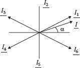
FIGURE 15.18 Possible positions of the current space vector in the complex plane.
The desired position of the space vector I is placed between two space vectors Ia and Ib, a,b = 1 − 6 (Figure 15.18) which represent the two states involved in the switching process. Writing the appropriate average relation provides
(15.5) |
where:
T = sampling period
ta = time assigned for the state Ia
tb = the time assigned for the state Ib
t0 = the time assigned for the state 10
For the peculiar case of AC/DC conversion, the proposed space vector PWM strategy takes into account both the prescription of the desired load current I and the input AC source unbalance or distortions through the instantaneous grid voltages. If we denote with E the measured AC-side converter input voltage, the relations for the time durations become:
(15.6) |
Vectors |
Switches |
I1 |
Sw1 + Sw6 |
I2 |
Sw3 + Sw6 |
I3 |
Sw3 + Sw2 |
I4 |
Sw5 + Sw2 |
I5 |
Sw5 + Sw4 |
I4 |
Sw5 + Sw4 |
I5 |
Sw5 + Sw4 |
I6 |
Sw1 + Sw4 |
I0 [1] |
Sw1 + Sw4 |
I0 [2] |
Sw3 + Sw4 |
Io [3] |
Sw5 + Sw6 |
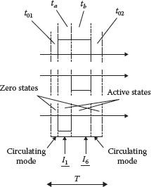
FIGURE 15.19 Pulse generation within the space vector modulation.
where
(15.7) |
While these equations are presented herein for the general theory development, they will be again exploited in Chapter 18 within a real practical application.
The duration t0 must be split into two zero states so that the transition from zero states to active states always involve only one switching. For the sake of simplicity and some generic optimization expectation, t0+ = t0_. Figure 15.19 shows as an example the synthesis of a current pulse whose associated space vector is placed between I1 and I6.
15.5 OPTIMIZATION OF PWM ALGORITHMS
Once the basic details for the Space Vector Modulation have been introduced, the algorithm can be improved further by association with certain optimization criteria [13,14,15,16]. Generally, the problems with PWM algorithms for the Current Source Inverter/Converter are related to the limited value of the switching frequency.
Since the AC-side of the Current Source Inverter/Converter is usually followed up with a LC filter, it is worth considering this filtering effect with a time-integral function of the inverter current. This function has the meaning of a voltage with gain depending to the values of capacitor C and grid line inductance (AC/DC case) or motor leakage inductance L (DC/AC case).
The representation of this time integral in the complex plane represents a polygonal locus with a shape close to an exact circle. The difference between the polygonal locus and the ideal circular locus represents the error and causes torque fluctuation in the motor drive case.
Several criteria can be considered to reduce the amount of harmonics generated by the noncircular locus of the time integral of switching currents. This is especially useful in the case of limited switching frequency. To help the understanding of these optimal methods, we will show herein results for the motor drive case. They can easily be expanded to the grid interface application.
The idea is to generate a regular polygonal locus that is to generate the space vector positions by a constant increment of the angular coordinate. Results from this method can only be improved further with a proper positioning of the active states over the sampling interval. However, the additional improvements are minimal.
Another optimization principle works close to the hysteresis control concept already known from switched mode converters. Maintaining the polygonal locus inside a circular corona is equivalent to reducing the output voltage ripple with effects in increasing the output power efficiency. Since the definition of this strategy is based on a geometrical analysis of the aforementioned constraint, it is worthwhile to use this criterion only for defining a polygonal locus with few sides, in the case of low carrier frequency. The resulting PWM pulse pattern is analogous to the case of delta or hysteresis modulation.
15.5.3 REDUCING THE LOW HARMONICS FROM THE GEOMETRICAL LOCUS
Since the AC-side low-pass filter is reducing the higher frequency harmonics of the current, it worth considering the possibility of choosing a locus able to eliminate the low harmonics. The degree of freedom comes from the relationship between the numbers of the edges from the polygonal locus that corresponds to the number of the low harmonics eliminated.
Previous research on the vectorial representation in the complex plane demonstrated that the rotational speed of the vector can be regulated by introducing operation within the zero-vector states. Observing these results outlines the difference between the previous optimal methods (circular corona and optimized geometrical locus) and the conventional Space Vector Modulation algorithms. A compromise solution can be developed in order to obtain the desired trajectories in the complex plane with a frequency modulation or a zero-vector split modulation. Results in the next section will limit to the zero-vector split modulation.
A comparison in between the harmonic performance for the methods described above is considered based on ideal PWM generation, without considering details of resonance between the filter components or gain loss within the inverter/converter.
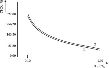
FIGURE 15.20 THD of the AC-side current for (1) space vector modulation, (2) trapezoidal PWM.
Similar to Chapter 3, Section 3.5.3, the Total Harmonic Distortion (THD) content of inverter output current defined as
(15.8) |
Figure 15.20 presents a direct comparison between the Space Vector Modulation and the trapezoidal modulation for a modulation index of 0.7, an output frequency of 20 Hz, and 24 pulses. It is demonstrated that the harmonics of the output current are lower than the classical trapezoidal modulation waveform and hence the efficiency of converter becomes better since the output current and voltage are nearly sinusoidal waves.
These results set the basis for understanding the benefits of the optimal methods mentioned above. To expand further the comparison while following the theory presented in Chapter 3, Section 3.5.3, a new harmonic performance coefficient is defined herein. The high order harmonics are attenuated by the AC-side filter and a more meaningful comparison is made by taking into account the harmonic order. The distortion coefficient is therefore defined by multiplying each frequency component with 1/(kω).
(15.9) |
Other similar distortion factors can be defined [15] to illustrate the influence of the filter:
(15.10) |
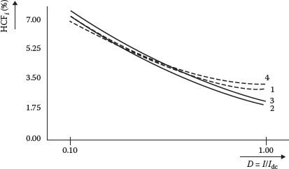
FIGURE 15.21 HCF for (1) = circular corona PWM with 24 edges polygonal locus; (2) = circular corona PWM with 36 edges polygonal locus; (3) = optimized geometrical locus with 36 edges polygonal locus; (4) = minimum square error method.
The following results are based on HCF coefficients only. If all symmetries in a three-phase system are considered, the harmonics used in the calculation of the HCF or DF coefficients can start from the 5th since there are no 2x or 3x harmonics. Otherwise, for a real case when symmetries cannot be considered, all harmonics, starting from the 2nd should be used in calculation.
The optimal methods can be compared with this HCF harmonic coefficient as well as content in the 5th and 7th harmonics of the output current (Figures 15.21, 15.22, 15.23, 15.24).
15.6 RESONANCE IN THE AC-SIDE OF THE CSI CONVERTERFILTER ASSEMBLY
Since the waveforms of the AC-side currents are made of pulses of current, the Current Source Converter is usually followed up with an AC filter, able to retain the higher harmonics of the current and to deliver a sinusoidal current into the AC circuitry. Since either the grid connection or the motor drive connected to the AC-side of the Current Source Converter is characterized with an inductance, the filter’s capacitance and such inductance constitute a resonant circuit [17,18] (Figure 15.25).
There are possible both hardware and control software solutions to prevent or damp resonance. An additional trap filter can be added to the system to a specified frequency. Or, the PWM and the filter components can be optimally selected to avoid having the resonance frequency near frequencies in the spectrum of the current coming into the filter from the Current Source Inverter. For instance, the 5th and 7th harmonics can be cancelled by proper PWM selection, while the filter (Lf + Cf) resonance can be selected at around 4.6 times the fundamental frequency [5].
The most academically challenging solutions are coming from proper design of the control loops. Usually such solutions revolve around the idea of introducing by control a virtual resistor along the hardware of the resonant filter so that the resonance yields damped [17]. A simple control structure is shown in Figure 15.26 for the case without any compensation. Since the converter’s output is a current, the controlled measure is a voltage across the load circuitry, measured across the capacitor Cf.
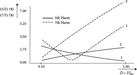
FIGURE 15.22 The 5th and 7th harmonics: (1) = circular corona PWM with 24 edges polygonal locus; (2) = minimum square error method with 24 edges polygonal locus.
If the AC-side is at the output of the converter and the load is a motor drive, the circuit equation for the load should contain the back-EMF voltage (e). Also the motor drive operation at different speed and load torque levels would imply change in the resonance frequency. This recommends further the use of a virtual resistance for damping of the resonance against other control methods.
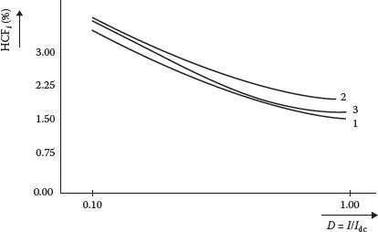
FIGURE 15.23 HCF for: (1) = circular corona with 48 edges polygonal locus; (2) = optimized geometrical locus with 36 edges polygonal locus; (3) = conventional SVM with 48 pulses.
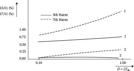
FIGURE 15.24 The 5th and 7th harmonics: (1) = circular corona PWM with 48 edges polygonal locus; (2) = minimum square error method with 48 edges polygonal locus.
The virtual resistor is set-up in software based on the feedback voltage Vc (Figure 15.27). A High-Pass Filter is applied to this voltage to avoid interference with the fundamental waveforms, and the current through the virtual resistance is calculated and accounted for within the current reference Iref. The HPF will degrade the transient damping performance for the virtual harmonic damper, especially when there is a disturbance from the filter capacitor feedback voltage. This is caused by the tradeoff between a smaller cutoff frequency in an HPF giving a slow response, and a larger cutoff frequency leading to high frequency signal distortions. A multitude of versions to this approach are reported in literature.
A very similar approach to resonance damping consists in generating a virtual negative inductance along the virtual resistance (Figure 15.28) [19]. The advantage is reduced loss in the Current Source Converter.
Alternative methods to eliminate the LC resonance include feed-forward control compensation using the LC filter model and control shaping using harmonic compensators. Such a compensator can be designed around the Posicast controller [17]. This is splitting any step input command into two intermediate steps. By considering the pause interval between the two steps as a parameter, the system response produced by the second step can cancel the resonant response excited by the first step, resulting in an oscillation-free step.
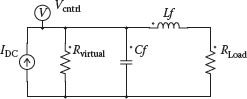
FIGURE 15.25 Circuitry illustrating the resonance with CSI-filter assembly.
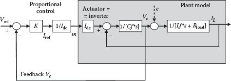
FIGURE 15.26 Simple model of the control system for the capacitor voltage.
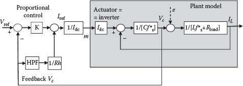
FIGURE 15.27 Control with compensation.
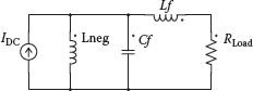
FIGURE 15.28 Circuitry illustrating the compensation with a virtual negative inductance.
Merits and drawbacks of the Current Source Converters have been explained and the basics of operation outlined. The current commutation between different switches needs attention for maintaining the current circulation. A large variety of PWM algorithms is available, many of them being derived from the implementation of PWM for voltage source inverters. Both passive and active approaches to damping the filter resonance are illustrated and their need shades the advantages of this class of converters.
More recent efforts consider multilevel current source converters where multiple stages are able to add the load current building up a current waveform with multiple steps. The optimization of the multilevel current waveforms can be achieved very similar to the optimization of voltage source converters at waveform level.
1. Trzynadlowski, A., 2010. Introduction to Modern Power Electronics. John Wiley and Sons, New York.
2. Holmes, D.G. and Lipo, T.A. 2003. Pulse Width Modulation for Power Converters—Principles and Practice. John Wiley and Sons, New York.
3. Wu, B., Pontt, J., Rodriguez, J., Bernet, S., and Kouro, S. 2008. Current-source converter and cycloconverter topologies for industrial medium-voltage drives. IEEE Trans. Industrial Electron. 55(7), 2786–2797.
4. Rey, J., Doval-Gandoy, J., Penalver, C.M., Lopez, O., Nogueiras, A., and Lago, A. 2005. Evaluation system for current source converter modulation techniques. 31st Annual Conference of IEEE Industrial Electronics Society. IECON 2005, pp. 5, 2005.
5. Suh, S., Steinke, J., and Steimer, P. 2006. A study on efficiency of voltage source and current source converter systems for large motor drives. 37th IEEE Power Electronics Specialists Conference. PESC’06, pp. 1–7.
6. Zhu, N., Xu, D., Wu, B., Zargari, N.R., Kazerani, M., and Liu, F. 2013. Common-mode voltage reduction methods for current-source converters in medium-voltage drives. IEEE Trans. Power Electron. 28(2), 995–1006.
7. Fukuda, S. and Hasegawa, H. 1988. Current source rectifier/inverter system with sinusoidal currents. IEEE IAS Annual Meeting, pp. 909–914.
8. Abu-Khaizaran, M. and Palmer, P. 2007. Commutation in a high power IGBT based current source inverter. IEEE PESC’07, pp. 2209–2215.
9. Halkosaari, T., Kuusel, K., and Tuusa, H. 2001. Effect of nonidealities on the performance of the 3-phase current source PWM converter. Power Electronics Specialists Conference, 2001. PESC. 2001 IEEE 32nd Annual, vol. 2, pp. 654–659.
10. Nonaka, S. and Neba, Y. 1991. Quick regulation of sinusoidal output current in PWM converter-inverter system. IEEE Trans. Industry Appl. 27(6), November/December, pp. 1055–1062.
11. Wu, B., Dewan, S.B., and Slemon, G.R. 1992. PWM CSI inverter for induction motor drives. IEEE Trans. Industry Appl. 29(1), January/February, pp. 64–71.
12. To, H.-P., Rahman, M.F., and Grantham, C. 2006. Modulation of current-source converters from gating signals for voltage-source converters. 37th IEEE Power Electronics Specialists Conference, pp. 1–6, 18–22.
13. Neacsu, D.O., Pastravanu, A., and Lucanu, M. 1993. Space vector PWM AC/DC converter. Proceedings of the Int’l Symposium SCS’97, Iasi, Romania, pp. 252–255.
14. Neacsu, D.O. and Donescu, V. Performance characterization of space vector PWM current source inverter. The 4th Int’l Conference OPTIM’94, Brasov, Romania, vol. 4, section F, pp. 109–114.
15. Espinoza, J.R. and Joos, G. 1997. Current-source converter on-line pattern generator switching frequency minimization. IEEE Trans. Industrial Electron. 44(2), 198–206.
16. Halkosaari, T. and Tuusa, H. 2000. Optimal vector modulation of a PWM current source converter according to minimal switching losses. IEEE 31st Annual Power Electronics Specialists Conference, PESC 2000, vol. 1, pp. 127–132.
17. Li, Y.W. 2009. Control and resonance damping of voltage-source and current-source converters with LC filters. IEEE Trans. Industrial Electron. 56(5), 1511–1521.
18. Neba, Y. 2005. A simple method for suppression of resonance oscillation in PWM current source converter. IEEE Trans. Power Electron. 20(1), 132–139.
19. Morsy, A.S., Ahmed, S., Enjeti, P., and Massoud, A. 2010. An active damping technique for a current source inverter employing a virtual negative inductance. IEEE PESC, pp. 63–67.