
![]()
A Patch-Bay Matrix Synthesizer
In this last chapter, we’re going to build a patch-bay synthesizer, much like the analog synthesizers. We’ll simulate the interface, but instead of an audio signal, we’ll pass connection data through the patch cords. The data will be sent to the computer so that the corresponding connections can be done in the program. We’ll use external chips (we’ll call them ICs from now on, which stands for integrated circuit) to extend both the analog and the digital pins of the Arduino for more available input and output. Finally, we’re going to use oscillators, filters, and envelopes to build the various parts of the program, which we have already used. We’ll be able to connect these parts between them through the patch-bay interface that we’ll build.
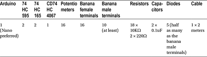
Table 10-1 lists the components we’ll need for this project. The 74HC595, 74HC165, and CD74HC4067 are ICs that you can find at your local electronics store or online. SparkFun has made a breakout board for each of these ICs, so you can choose those if you like. The 74HC595 and CD74HC4067 circuits will be built using these breakouts, as well as the ICs, since Fritzing (the program with which all the circuits in this book are built) provides parts for these breakouts. But the 74HC165 will be built with only the IC, because there’s no part for the breakout in Fritzing. The pin names and numbers of the breakouts and the ICs will be mentioned in detail. If you have the data sheet for each IC, you’ll be able to build the circuits by following the instructions in this chapter. (I’ve used the data sheets provided by SparkFun.) The breakouts have the pin names printed on the circuit board. If you use the breakouts, make sure that you solder male headers on the pins of the board; otherwise, you won’t get proper connections when you use them with a breadboard.
The banana male terminals will be used to create the patch cords. To have five patch cords, we’ll need 10 male bananas. The more you have, the better, since you’ll be able to make more connections. You can make a few in the beginning and then make more at some later point.
Table 10-1. Parts List for the Patch-Bay Synthesizer
What We Want to Achieve in this Chapter
Before we start, let’s first visualize what we really want to achieve. Figure 10-1 shows a Pd patch with a few components that are not connected between them. We have two oscillators (a sine wave oscillator, which can have its phase modulated, and a sawtooth oscillator), a lowpass filter, an envelope, and the [dac~]. You might want to play around a bit with this patch and try different connections between these elements. Connect the output of the sawtooth oscillator to the lowpass filter and then to the phase of the sine wave oscillator. Connect the envelope to the amplitude of the sine wave oscillator (you’ll need to add a [*~ ] for that). Connect the envelope to the output of the sawtooth and then to the phase of the sine wave. There can be quite a few connections, which can yield pretty interesting results. By the end of this chapter, we’ll have built an instrument in which these connections were made using real cables, without the clicks we get when we dynamically change a Pd patch with the DAC on.
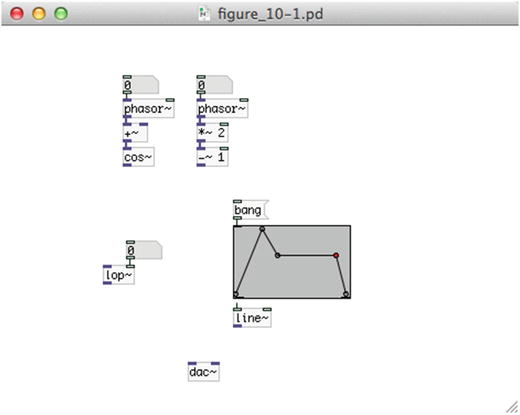
Figure 10-1. A Pd patch without predefined connections
This chapter is rather long and probably the most complex of all the chapters in this book. What follows are certain techniques that deal with expanding the analog and digital pins of the Arduino, and making a patch-bay matrix. After that, we’ll go through the implementation in Pd. Read carefully through the chapter and be very careful when you’re building the circuits. If something doesn’t work for you, read again and retry the circuits until it works.
Extending the Arduino Analog Pins
The Arduino Uno has only six analog pins, which are quite few. Even the Nano, which has eight, is rather limited for some projects. To solve this problem we can use multiplexers. These are chips that can take up to a certain number of analog inputs (depending on the number of channels they have) and route them sequentially to one analog pin of the Arduino. The CD74HC4067 multiplexer has 16 channels, which means that with one of them we can have 16 analog inputs that will occupy only one analog pin of the Arduino. Of course, this multiplexer doesn’t come so cheap, as it needs four digital pins to control the sequence of its inputs. To better visualize how this chip works, let’s see it wired in Figures 10-2 and 10-3.
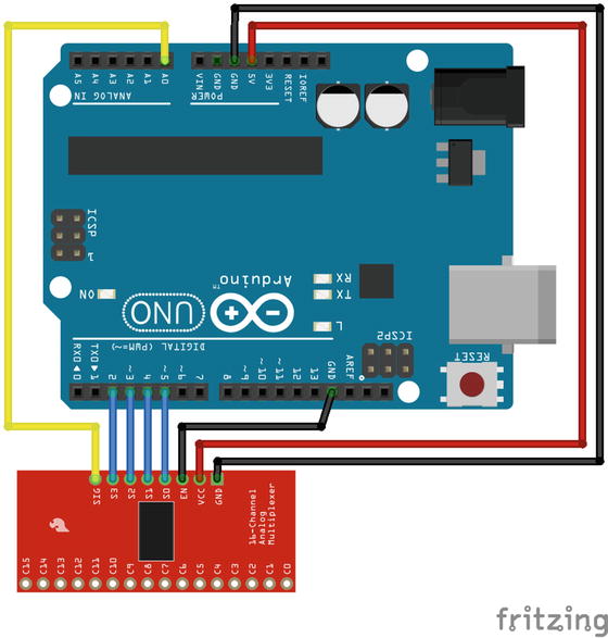
Figure 10-2. The CD74HC4067 multiplexer breakout board wired to an Arduino Uno
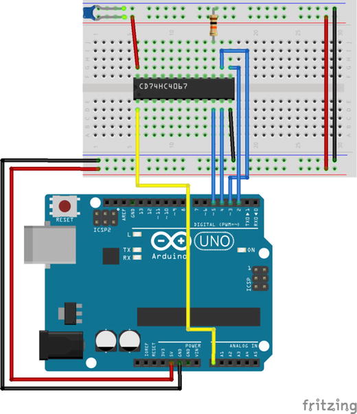
Figure 10-3. The CD74HC4067 multiplexer IC wired to an Arduino Uno
In Figure 10-2, the breakout version of the chip is used and Figure 10-3 uses the IC (mind that the actual IC is a bit thicker, but there’s no dedicated part in Fritzing, only a generic IC part). Just a reminder on pin numbering, all ICs have either a notch on one side, or a dot, which indicates the first pin. The dot is usually on the side of the first pin. If the IC has a notch, the first pin is the one on the left side of the notch. Then pins are numbered sequentially around the pin. In Figure 10-3, the first pin is the leftmost pin on the lower side, and the successive pins are on its right. These are the first twelve pins. On the upper side, pin 13 is the rightmost pin, and the leftmost pin is the last one, pin 24.
There are no potentiometers wired to the breakout or IC for now, just to keep the circuit a bit clearer. On the bottom side of the board we have the 16 input pins, C0 to C15 (on the IC these are pins 9 to 2 and 23 to 16 labeled I0 to I15). On the top side, we have the SIG pin (signal pin, on the IC this is pin 1 labeled Common Input/Output), the S0 to S3 pins (on the IC they are pins 10, 11, 14, 13), the EN pin (enable pin, on the breakout this is pin 15 labeled E), and the VCC and GND pins (voltage and ground, on the IC these are pins 24 and 12). If you’re using the IC instead of the breakout, you might want to connect pin 15 of the chip (E) to ground via a 10KΩ resistor, and use a 0.1μF capacitor between the voltage and the ground, close to pin 24 (VCC). The resistor and capacitor are included in the breakout board used here.
The pins C0 to C15 (or I0 to I15) take analog input. We’ll connect the potentiometers to these pins. The SIG pin connects to one of the Arduino’s analog pin. This pin will transfer the signals of the pins C0 to C15 to the Arduino. The four control pins (S0 to S3) are connected to four digital pins of the Arduino, where S0 connects to digital pin 5, S1 connects to pin 4 and so forth. These pins will determine which of the input pins (C0 to C15) will be connected to the SIG pin. The EN pin enables or disables the device, where with a low signal (zero volts or ground) it is enabled (this is referred to as enable low), and with a high voltage it is disabled. We won’t deal with disabling the device, so we’ll always have this pin wired to ground (with a 10KΩ resistor for the IC circuit).
To understand how the S0 to S3 control pins work, I need to talk a bit about binary numbers. Listing 10-1 shows the first 16 numbers (including 0) in binary form.
To make the connection between these numbers and the control pins of the multiplexer, think of 0s as low voltage, and 1s as high voltage, meaning that with a 0, a digital pin will be LOW, and with a 1, it will be HIGH. The four control pins of the multiplexer, S0 to S3, and the four digital pins of the Arduino used in Figures 10-2 and 10-3 (pins 2 to 5) are paralleled with the digits of the numbers in Listing 10-1. What I mean by that is that the rightmost digit of a value represents the state of the pin S0 of the multiplexer and digital pin 5 of the Arduino, the digit on it left represents the state of the pin S1 and digital pin 4 and so forth.
This means that to connect pin C0 of the multiplexer to its SIG pin, which connects to analog pin 0 of the Arduino, we need to set all four of the Arduino digital pins that control the chip LOW. If we want to connect C1 to the SIG pin of the chip, we need to set digital pin 5 of the Arduino HIGH and the other three LOW. If we want to connect C2 to the SIG pin, we need to set digital pin 4 HIGH and digital pins 5, 3, and 2 LOW. Hopefully you understand the mechanism behind this. Since we’re using digital signals to control the multiplexer, and since the multiplexer has 16 channels, it makes sense as to why we need four control pins, since 2 to the fourth power yields 16, which means that with four digital pins we can have 16 different combinations. If the multiplexer had eight channels, we would need three control pins, since 2 to the third power yields 8.
Writing Code to Control a Multiplexer
With some explanation, the mechanism of a multiplexer might seem rather simple and clear. But how can we implement this in Arduino code? One way would be to write the binary values in Listing 10-1 to a two-dimensional array and call each digit of each value to set the control pins of the Arduino appropriately. This doesn’t look very elegant though, and the coding we would need to do would be a bit more than necessary. We want to read the values of the pins C0 to C15 sequentially and store them in an array, which we’ll then transfer to Pd. To do this, we’ll run a for loop. We’ll use the loop’s incrementing variable to set the control pins of the Arduino. Listing 10-2 shows the code.
This code is written in such a way that will work with any number of multiplexers, and the multiplexers can have any number of channels (usually it’s eight or sixteen), as long as all multiplexers used have the same number of channels. (You could write code for multiplexers with different number of channels, but it would be slightly more complex, and we shouldn’t really care about this right now, since we’ll use one multiplexer.)
Defining Preprocessor Directives
Already from line 2, we meet new things. This is a preprocessor directive. It is not regular C++ code, but a directive for the preprocessor. This means that this line will be handled before the compilation of the code. We’ve used the #include preprocessor directive in Chapters 3 and 5, where we used the SofwareSerial library. Here we use the #define preprocessor directive to define what is called a macro. The #define directive is used to define constants. What it actually does is to replace text. Therefore, this line sets that wherever we use LOG2(x) in our code, it will be replaced by (log(x) / log(2)). This last definition uses the log built-in function of the Arduino language to create a function that returns the base 2 logarithm of a given value. The log function returns the natural logarithm (base e), so to get the base 2 logarithm of a value, we must divide the natural logarithm of this value, by the natural logarithm of 2. Since this function is a one-liner, we can define it as a macro, instead of the way we’ve been defining functions up until now.
We need the base 2 logarithm to get the number of control pins we need for the multiplexer. If your math is rusty, all you need to know is that the logarithm of a certain value yields the number we need to raise the base to get this value. I’ve already mentioned that we need four digital pins to control the multiplexer because it has 16 channels, and since 2 to the fourth power yields 16, the base 2 logarithm of the number of channels (which is 16) will yield 4 (which is the number of control pins we need). If the multiplexer we use had 8 channels, then the base 2 logarithm of 8 would yield 3, which would be the number of control pins we would need in this case. This way, we can limit the number of parameters we need to change manually in case we use multiplexers with a different number of channels.
If you’re using an older version of the Arduino IDE, this will probably not work. In this case, don’t include it in your code, and in line 9, you’ll have to hard code the value of the num_ctl_pins constant to 4, instead of using this custom log base 2 function.
In lines 5 and 7, we define the number of multiplexers we’ll use and the number of channels these multiplexers have. Line 9 is where we use the macro function we’ve defined in line 2. This line uses the constant that holds the number of channels of the multiplexer and yields the number of control pins this multiplexer has. If we hadn’t defined the macro function, we’d have to hard-code this line, meaning that if we used this code with a different multiplexer, which had another number of channels, we would have to change this line manually.
In line 13, we define the number of bytes we’ll be transferring to the serial line. (The earlier comments explain why we need a particular number of bytes. We’ll use the Serial.write function, so we need to break the analog values into two.) In line 16, we define the array that will be transferred over serial. Line 19 defines an array that will hold the numbers of the control pins, but since we don’t want to hard-code things, we’ll set these numbers in the setup function using a for loop. In line 22, we define an array that will hold values, which will be used in the main for loop that reads the values of the multiplexer. The values of this array will be used to translate the decimal value of the incrementing variable of the for loop to binary. We’ll see how this works in detail further on.
Setting the Control Pin Numbers and the Binary Masks
In the setup function we have two things, a for loop and the initialization of the serial communication. In the for loop, we set the values of the last two arrays we created in lines 19 and 22. I’ve stated that the control_values array will be used to translate decimal values to binary. To do this we’ll need to mask the decimal values by the values of the array using the bitwise AND (&). After this loop has finished, the array will have the following values stored: 1, 3, 7, 15. Think how this is achieved (hint, the pow function raises its first argument to the power of its second argument). We still don’t see the workings of this value translation, because it happens in the main loop function. The control_pins array will store these values: 5, 4, 3, 2, which are the numbers of the control pins. Again, we’ll see further on why they are stored from the greatest number to the smallest.
Reading the 16 Values of the Multiplexer
In the main loop function, we have three nested for loops. The first one, in line 38, goes through all the multiplexers we’re using (in this case, it’s only one). Note its incrementing variable, i, as we’ll need to keep it in mind to understand how these nested loops work. The second loop, which runs inside the first, in line 40, goes through all the channels of the current multiplexer. Its incrementing variable is j. The third loop, in line 41, goes through the four control pins, and its incrementing variable is k. The important lines we need to understand are 44 and 46. In line 44, we read the following:
digitalWrite(control_pins[k], (j & control_values[k]) >> k);
In this line we have two bitwise operations, the bitwise AND and the bitshift right. Just as a reminder, bitwise ANDing two values results in comparing the bits of each value and acting on them independently of the rest of the bits in a Boolean fashion. When both bits are 1, the resulting bit will be 1. When one of the bits or both of them are 0, the resulting bit will be 0. For example, bitwise ANDing the following two values:
00101101
10011011
will result in this value:
00001001
Shifting the bits of a value by a certain number of places results in just that: the bits of the value being shifted. If we shift the bits of the following value:
00101101
by one place to the right, we’ll get this:
00010110
What happens is that the bits don’t wrap around the end and beginning, but the new bits that are introduced (in this example, it’s the leftmost bit) are 0.
All these operations are possible in all kinds of numeric representations, be it binary, decimal, hexadecimal, or octal. Regardless of the numeral system, these operations act on the bits of values (since we’re dealing with computers, all values are eventually binary).
Now let’s get back to line 44. In the first iteration of the first two loops, all iterations of the third loop will result in the second argument to the digitalWrite function being 0. This is because j will be 0, and no matter what value we bitwise AND it with and how many places we shift its bits, it will always result in 0. The loop of line 41 will then set digital pins 5, 4, 3, and 2 LOW (these four numbers are the values of the control_pins array).
This is where we need to keep track of the values of the incrementing variables of the three loops. At the first iteration of the loop of line 40, in all iterations of the loop of line 41 j will be 0, but k will take the values 0 to 3. In the second iteration of the loop of line 40 j will be 1. In the first iteration of the loop of line 41, the second argument to the digitalWrite function will be 1. This is because we’re bitwise ANDing 1 with 1, which results in 1, and we’re shifting its bit by 0 places, leaving the value 1 intact. So line 44 will set digital pin 5 HIGH. The other three iterations of the loop of line 41 will result in 0, because we’ll be masking 1 with the values 3, 7, and 15, and we’re shifting their bits by 1, 2, and 3 places. To visualize it, the numbers 1, 3, 7, and 15 are shown in listing 10-3 in both binary and decimal.
Don’t forget the bit shifting after we bitwise AND the two values. If j is 1, bitwise ANDing it with 3, 7, or 15 will yield 1. But shifting their bits to the right will again result in 0. Take some time to think and understand how these nested loops result in setting the control pins to the values we want. You might need to write the values down and compare them. A binary to decimal converter (and the other way round) will also be helpful here.
Go to line 46. This is where we’re reading the Arduino analog pin. This happens at all 16 iterations of the loop of line 40. But instead of using the j variable to control the analog pin that we’ll be reading, we’re using i, which is 0 (because the loop of line 38 runs only once in our example), since all 16 inputs of the multiplexer end up in analog pin 0 of the Arduino. After we read the Arduino analog pin, we’ll store the value we get every time to a successive index of the transfer_array.
In our example, we’re using only one multiplexer, so i will always be 0. If we were using more multiplexers, in the second iteration of the loop of line 38, i would be 1, so in the loop of line 40, we would connect all the inputs of the second multiplexer to analog pin 1 of the Arduino. We would read these values and again store them in successive indexes of the transfer_array. This way, we could use the same four Arduino digital control pins for as many multiplexers that we’re using. When reading the inputs of one multiplexer we don’t care about the input from other multiplexers because we aren’t reading the Arduino analog pins the other multiplexers are wired to.
Wiring 16 Potentiometers to the Multiplexer
We’ve already seen how to wire the multiplexer to the Arduino, but I’ll show the circuit again, this time with the 16 potentiometers wired to the multiplexer (only with the breakout this time, but it should be easy to wire the potentiometers to the IC as well). It is shown in Figure 10-4. It might look a bit scary, but the logic is simple. Each potentiometer’s wiper (the middle leg) is wired to one input pin of the multiplexer, and the side legs are wired to the voltage and ground provided by the Arduino. In Figure 10-4, the rightmost potentiometer is the first one, and this is only because of the orientation of the multiplexer breakout. It is oriented like this because it was easier to parallel its control pins with the binary values in Listing 10-1.

Figure 10-4. Wiring up the 16 potentiometers
Mind that if you’re using a long breadboard (which you most likely are), the ground and voltage lines on both sides of the board are usually cut in the middle of the board. If you provide voltage and ground on one side of the board, this will go up to the middle of it and the other side won’t get it. Figure 10-4 shows how you should connect both sides of voltage and ground of the board. This is done on the lower side of the board where no part is actually wired (all potentiometers get voltage and ground from the upper side of the board). This is done this way because it’s a bit clearer to show how to wire a long breadboard as the upper side of it is filled with jumper wires.
Reading the 16 Potentiometers in Pd
Since we’ve used the Serial.write function in the Arduino code, it’s easy to guess that in Pd we’ll use the [serial_write] abstraction to receive the potentiometer values. The patch is shown in Figure 10-5. There’s not much to say about this patch, we’ve already received analog input from the Arduino using this abstraction. We need to set only two arguments to [serial_write] “analog 16” and it will work.
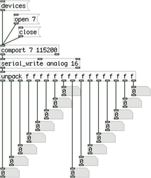
Figure 10-5. Pd patch that reads the 16 potentiometers of the multiplexer
Extending the Arduino Digital Pins
There are two kinds of ICs that enable extending Arduino digital pins: one for input and one for output. These ICs are called shift registers, because they shift their bits in the register. You don’t need to know what this exactly means and how it is done, it’s just mentioned to explain their name. One nice feature that we do care about is that these ICs are being daisy chained. This means that if we want to use more than one, we don’t need to occupy more pins on the Arduino, because they talk to one another, passing data through the chain.
Using the Input Shift Register
We’ll start with the input IC, which is the 74HC165 shift register. This chip has eight inputs, so we’ll use it with eight push buttons first, and then we’ll add another chip and another eight push buttons to see how we can daisy chain them and control them this way.
Writing the Arduino Code
We’ll start with the Arduino code, which is shown in listing 10-4.
Including the SPI Library
In line 1, we use the #include preprocessor directive to include the SPI library. SPI stands for Serial Peripheral Interface. It is a communication interface used for short distance communication. This is a standard library in the Arduino language, but we still need to include it this way. We’ll use a class from this library to send bytes to the shift register, as it facilitates the control of the chip to a great extent. We’ll also use this library to control the output shift registers, almost the same way.
The Arduino provides a built-in function to achieve what we want, shiftIn(), but it is slower than using the SPI library, and not as intuitive. Its advantage over the SPI library is that with this function we can use any pin of the Arduino to control the shift register, whereas with the SPI we need to use specific pins, as the former is a software implementation and the latter is a hardware implementation. For the project we want to build, using the specified pin of this library is not a problem as we don’t need them for something else, so it servers our purposes just fine.
Defining the Global Variables and Setting up Our Program
In lines 3 to 6, we define our global variables. The first variable we define is the latch_pin. We’ve named this variable this way because of the pin it connects to on the shift register. This pin is called the latch pin because it is the pin that will trigger output from the shift register into the Arduino when it goes HIGH. Then we define the number of chips, which is the only variable we’ll change when we use two chips, and depending on this value, we define the number of bytes we’ll be transferring to Pd over serial. There are two different ways that we can send the data of the shift register to Pd. This chip sends in one byte to the Arduino, which represents the states of its eight input pins (a byte consists of eight bits). We can either break this byte into its bits in the Arduino, using the bitRead() function, or we can send the whole byte to Pd as is, and break it down in there. We’ll go for the second approach because it’s similar to the technique we’ll use in our patch-bay synthesizer for detecting connections. Finally, we define the array that will be transferred to Pd over serial.
The first thing we do in the setup function is to begin the communication of the SPI library. We do this by calling the begin function of the SPI class. Notice that this is similar to beginning the serial communication of the Serial class, only for the SPI class we don’t define a baud rate, but we leave the parenthesis of the begin function empty. Then we set the mode of the latch_pin, which must be OUTPUT, and finally we begin the serial communication.
The Main loop of the Program
In the main loop function, apart from defining the index offset we use when we transfer data with Serial.write, we also define a byte that will store the byte received from the shift register. What we then do is drop the latch_pin LOW and then immediately bring it HIGH. This will trigger output from the shift register into the Arduino, as stated earlier. Once we do that, we run a loop to read data from all the chips in our circuit (which is only one for now). Inside this loop, we store to the in_byte variable the byte returned by the SPI.transfer function. We need to provide an argument to this function call, but since we don’t need to write to a device (as we’ll do when we’ll use the output shift registers), we provide a 0 as the argument. This function will then read the data received in the digital pin 12 of the Arduino, which is the MISO pin (MISO stands for Master In Slave Out). This pin receives the bits sent by the shift register and returns a byte for every eight bits. This byte is stored in the in_byte variable and then we use the same technique with the analog values to store it in the transfer_array. Notice that we mask in_byte with 0x7f instead of 0x007f because we’re now dealing with bytes and not ints. An int is two bytes long, and two digits of a hexadecimal number cover the range of one byte. When we mask an int with a hexadecimal value, we must provide four digits to this value, but with a byte, we only need two digits.
Even though we’re reading switches, which are digital, we send the states of eight switches in one byte. This means that this byte can possibly take the value of the start character, which is 192. To avoid this we use the technique of breaking up the byte to two bytes with the eighth bit always low (refer to Chapter 2 if you don’t remember how this works). In this sketch, we’re using one shift register only, so we could have just sent this byte as is to Pd. Later on, we’ll use two shift registers and sending bytes without a start character won’t be possible. Also, we want to make the code flexible so we can use the same sketch for any number of chips, only by changing the num_of_chips constant in line 4, so not using a start character would make this impossible. This means that we’ll receive the byte of the shift register in Pd as if it was an analog value.
Making the Input Shift Register Circuit
The circuit for this IC is shown in Figure 10-6. Each time that we used push buttons in this book, we used the integrated pull-up resistors of the Arduino. With the shift register, we don’t have this capability so we need to use external resistors. This time we’ll use pull-down resistors as you can see in Figure 10-6. One leg of each push button is connected to a 10KΩ resistor, which is connected to ground. The other leg is connected to the 5V. There’s one more 10KΩ resistor connecting the pin 15 (CE) of the chip to ground. There’s also a 0.1μF capacitor between ground and 5V. You should place this capacitor as close to the 5V pin of the chip as possible. If you’re using the breakout, the 10KΩ resistor of the pin 15 and the capacitor are on the circuit board (you don’t even have a label for pin 15, it’s not broken out).
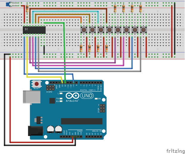
Figure 10-6. Input shift register circuit
Pin 1 of the chip (PL on the chip’s data sheet, SH/LD on the breakout board) connects to pin 9 of the Arduino. This is the latch pin. Pin 2 of the chip (CP on the chip, CLK on the breakout) connects to Arduino’s pin 13. This is the Arduino’s SCK pin (Serial Clock). Quoting from the SPI library page of the Arduino web site, this pin sends “the clock pulses, which synchronize data transmission generated by the master.” Pin 9 of the chip (Q7 on the chip, SER_OUT on the breakout) connects to Arduino’s pin 12, which is the MISO pin, as I’ve already mentioned. Pin 8 is the ground pin and pin 16 is the voltage pin.
Connect the leg of each push button that connects to the pull-down resistor to the chip’s pins 11, 12, 13, 14, 3, 4, 5, and 6. These are the pins D0 to D7 (on the breakout, they’re labeled A to H).
The Pd Patch That Reads the Eight Switches
Figure 10-7 shows the Pd patch that breaks the incoming byte to its bits. As I’ve already said, we’re using the [serial_write] abstraction and we’re receiving the byte of the eight switches as if it was an analog value, since we’re breaking it up to two bytes. Every time we receive a new byte, we run a loop that iterates eight times (as many as the pins of the chip). This loop raises 2 to an incrementing power, starting from 0 and ending at 7 (mind that [swap 2] has both its outlets connected to both inlets of [pow]). The result of this yields the values 1, 2, 4, 8, 16, and so forth, until 128. We bitwise AND these values with the incoming byte. If the result is not equal to 0 (which is checked by [!= ] - this means not equal to in C), it means that the corresponding push button is being pressed, otherwise it is released. We’re using the same incrementing value of [loop] to route each value to the appropriate toggle on the bottom side of the patch.
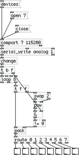
Figure 10-7. Breaking the byte sent from Arduino to its bits
Upload the sketch on your Arduino board and test it with this patch. You should see the corresponding toggle of each push button you’re pressing “going on.” Of course, you can press more than one push button at a time, you can even press them all together. They are independent of each other. We can see that with only three digital pins of the Arduino we can have eight digital inputs. Actually, we can have much more than that, and this is the next thing we’re going to do— add another input shift register to our circuit.
Daisy Chaining the Input Shift Registers
A very nice feature of these shift registers is that they can be daisy chained. This way, we can extend the digital inputs of the Arduino even more, while using the same three digital pins of it. We don’t need to show the code here, all you need to do is change line 4 in Listing 10-4 and set the num_of_chips constant to 2. This enough for the code to work. We need to check the circuit. This is shown in Figure 10-8. I’ve used curved wires for the second chip so you can easily distinguish its connections from the first.
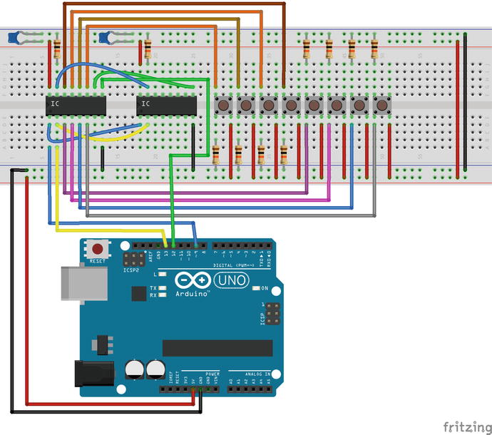
Figure 10-8. Daisy chaining two input shift registers
The push buttons of the second shift register are not included because it would look quite messy. Pins 1 and 2 (PL and CP on the chip, SH/LD and CLK on the breakout) of the second chip are connected to the same ones on the first chip. Pin 9 of the second chip (Q7 on the chip and SER_OUT on the breakout) connects to pin 10 of the first chip (DS on the chip and SER_IN on the breakout). Pin 15 of the second chip (CE on the chip, CLK on the breakout) connects to ground via a 10K resistor, but must also connect to pin 15 of the first chip (the resistor is included in the breakout).
The labels of the breakout board are more intuitive here. SER_OUT stands for serial out. This pin sends the byte of the chip serially out. SER_IN stands for serial in. This pin receives bytes serially from other chips and passes them through its own SER_OUT pin. This way, we can use many chips daisy chained where the byte of the last chip will pass through all the other chips until it reaches the Arduino. The rest of the wiring for the second chip is the same as with the first (including another eight push buttons and all the resistors and the capacitor – remember that if you’re using the breakout board, the capacitor and the resistor that connects to the CE pin are included in the board).
Extending the Pd Patch to Read 16 Push Buttons
As with the circuit and code, the additions we need to make to the Pd patch are just a few. The patch is shown in Figure 10-9. This time we’ll be receiving two bytes (actually, four bytes broken into two bytes each, which are being assembled inside the [serial_write] abstraction), so we need to change the second argument to [serial_write] from 1 to 2. Then we [unpack] these two bytes and we go through the same process for each.
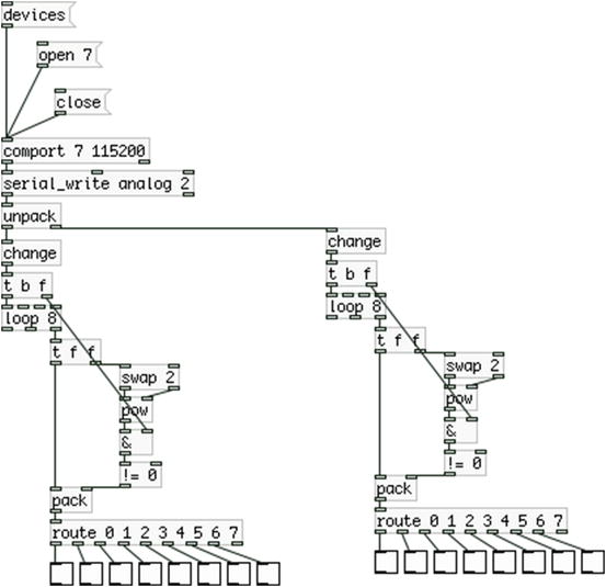
Figure 10-9. Reading 16 push buttons from two shift registers
Now on the right side we have the second shift register and on the left side we have the first one. With these two chips and only three Arduino digital pins, we already have 16 digital inputs, more than the digital inputs of the Arduino itself! Probably you can see how much potential this chip and technique give us. Getting digital input doesn’t limit us to just using push buttons or switches, further on we’ll see how we can use these chips to accomplish the patch-bay matrix for our synthesizer.
Using the Output Shift Register
Let’s move on to see how the output shift register works. This is the 74HC595 chip, and like with the others, there’s a breakout board by SparkFun for it. It is very similar to the input one. Again, we’ll use only three pins of the Arduino for as many shift registers we use. We’ll again use the SPI library to control these devices in a similar way with the input shift registers.
Writing the Arduino Code
Listing 10-5 shows the code for a basic control of one output shift register.
In this code, we’re not controlling the chip through the computer so there’s no serial communication involved here. In line 5, we define an array of the data type byte to hold the bytes to be transferred to the chips (for now it’s only one). What we want to do is light up eight LEDs one after the other, back and forth. This means that we need to run two different loops, one for lighting up the LEDs in an ascending order, and one in a descending order. To avoid writing the same code twice, we define a function that will write the byte to the shift register in line 7, set_output.
This function is very similar to the way we read bytes from the input shift registers. There are only three differences. First, we set the latch_pin LOW, then we write the bytes, and then we set it HIGH. In the case of the input shift registers, we would set this pin LOW, then HIGH to trigger the output of the chips, and then we would read the bytes in the Arduino. Now we need to write the bytes to the chip and then trigger its output (which will go to the LEDs, not the Arduino). The other difference is that we’re not receiving any value from the SPI.transfer function, but we only write a value through it, so we’re not assigning whatever this function returns to any variable, as we did with the input shift registers. A last minor difference is that in the loop that writes the bytes to the chips, we set the loop’s variable i to its maximum value and we decrement it, instead of starting it from 0 and increment it. This way, the bytes we’ll write will go to the chips we expect. If we run this loop the other way round, the first byte would go to the last chip of the chain (in case we use more than one chip).
The bitSet and bitClear Functions
We encounter two new built-in functions of the Arduino language: bitSet and bitClear. These functions operate on the bits of a given value. bitSet writes a 1 to a specified bit of a given value, and bitClear writes a 0. They take two arguments: the value to write to its bit and the bit of that value to write to. These functions are being used in the main loop function where we run two nested loops where the first one iterates through all the chips of our circuit and the second one iterates through all the pins of each chip.
In line 23, we make sure that we’re not at the first chip, so that we can set a 0 to the byte of the previous chip. (If we are at the first chip, there’s no previous chip and this line would try to access a byte beyond the bounds of the out_bytes array, causing our program to either not run properly, or even crash). Then we iterate through the pins of each chip. In line 26 we check if we’re not at the first pin (much like the way we check if we’re not at the first chip), and if we’re not, we write a zero to the previous pin, so we turn that LED off. In line 28, we write a 1 to the current bit of the current byte, causing the LED to go on and then we call the set_output function. Only when this function is called will the values we’ve set to the out_bytes array take effect on the LEDs.
In line 34, we run a loop the other way round, which starts from the last chip and goes down to the first. Now, instead of checking if we’re not at the first chip, we check if we’re not at the last one. The same goes for the pins. This way, we can erase the previous pin of the loop (which is actually the next pin of the chip). In both loops, there’s a small delay of 200 milliseconds to make the whole process visible. If we don’t include this delay, all LEDs will look like they’re constantly lit, but they will be dimmed (it will work like doing PWM to an LED). This doesn’t mean that we can’t light up more than one LED at a time. On the contrary, shift registers provide independent control of each of their pins.
Making the Output Shift Register Circuit
Fritzing provides a component for the breakout board of the output shift register, so we’ll use both this and the IC here. The circuit with the breakout is shown in Figure 10-10 and with the IC in Figure 10-11. A cool feature of the breakout board (apart from saving us from some wiring) is that it enables daisy chaining by breaking out the pins of the chain to the left and right of the board. The way the board is oriented in Figure 10-10, the first chip would take input from its right side, and it would then give output to the next chip from its left side. This way, it is extremely easy to daisy chain these devices.
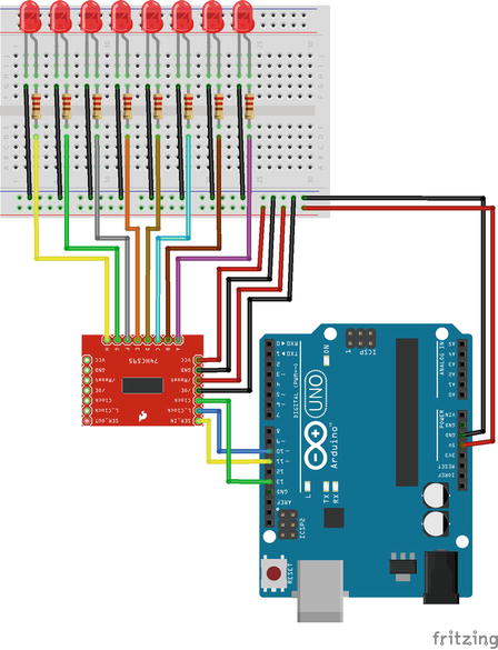
Figure 10-10. One output shift register breakout circuit
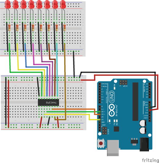
Figure 10-11. The output shift register IC circuit
On the left side of the board, starting from top we have the voltage pin (VCC, pin 16 on the IC), which connects to the voltage. Then we have the ground pin (GND, pin 8 on the IC) which connects to ground. The next pin is the /Reset pin (pin 10 on the IC labeled SRLCR), which connects to the voltage. The pin after that is the /OE (this stands for Output Enable and it is pin 13 on the IC) which connects to ground. Then we have the Clock pin (pin 11 on the IC labeled SRCLK). This pin connects to digital pin 13 of the Arduino. This is the same pin as pin 2 on the input shift register, which is marked as CLK on the breakout and CP on the chip. This pin receives the clock pulses from the Arduino to be synced. After the Clock pin we have the L_Clock pin (pin 12 on the IC marked RCLK), which connects to digital pin 10 of the Arduino. This latch pin triggers the output on the chip. Last pin is the SER_IN, which stands for serial in (pin 14 on the IC labeled SER). This pin connects to digital pin 11 of the Arduino, which is the pin called MOSI, which stands for Master Out Slave In. It’s the opposite of digital pin 12, which is the MISO that we’ve used with the input shift register. The MOSI pin sends out bits to the devices, where the latter forms a byte from these bits and output it when their latch pin goes HIGH. We don’t see the workings of the MISO and MOSI pins because it’s being taken care of by the SPI library. This makes the whole process of using such devices very easy and intuitive (as well as fast). Before you test the program, note that the resistors used in this circuit are 220Ω. Run the sketch in Listing 10-5 and you should see the LEDs go on one by one.
Daisy Chaining The Output Shift Registers
Daisy chaining the output shift registers is similar to the input ones. As far as the code is concerned, all we need to do is set the num_of_chips constant in line 4 to 2 and it will work. If you’re using the breakout for the shift register, the circuit is very simple. It is shown in Figure 10-12. The left side of the first breakout connects straight to the right side of the second breakout. If you have the ICs instead of the breakouts, check Figure 10-13. The second chip has the same connections as the first, except from pin 14 (marked SER) which, instead of connecting to the Arduino MOSI pin, connects to pin 9 (labeled QH’) of the first chip. Pin 9 outputs the overflowing bits a chip receives. So, if we send two bytes from the Arduino to the chips, the bits of the second byte will overflow through the first chip into the second. This pin on the breakout is labeled SER_OUT, which stands for Serial Out. In Figure 10-13 the LEDs of the second chis have been omitted to keep the circuit a bit clear. Their wiring is identical to that of the first chip.
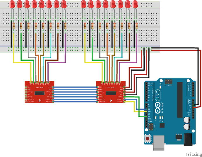
Figure 10-12. Daisy chaining two output shift register breakouts
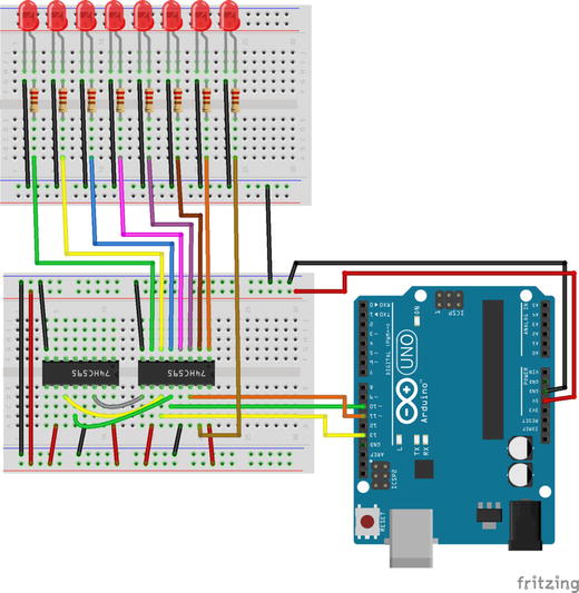
Figure 10-13. Daisy chaining two output shift register ICs
If you’re using the breakouts, you can use angled headers to connect the two boards. This feature makes it extremely easy to use as many shift registers as you want. The same applies to the breakouts of the input shift register breakouts.
Combining the Input and Output Shift Registers
It should be fairly easy to combine the two kinds of shift registers. Listing 10-6 shows the code.
Now we define a function for each type of shift register, so that we don’t include their code in the main loop function. These functions are defined in lines 11 and 18. Take a minute to compare them and to compare the get_input function to the part of the code in Listing 10-4, where we were reading the incoming bytes of the input shift registers.
We also define one array per shift register type, in lines 6 and 7, as well as an array for transferring data. The latter has a different size than the first two. In this sketch, we suppose we use the same number of chips for both input and output, because we’ll control the LEDs of the output with the push buttons of the input, so we need one push button per LED.
In the main loop function, we first call the get_input function to get the input from the push buttons. Then we run a loop to copy the bytes that were written in the in_bytes array to the transfer_array. We do that because we’ll need these bytes intact to control the LEDs. If we used the transfer_array straight in the get_input function, we wouldn’t be able to control the LEDs properly, as we would have split the bytes to two to transfer them over the serial line. In this same loop, we copy the bytes of the in_bytes array to the out_bytes array. This step could have been avoided and we could have used the in_bytes array in the set_output function. This way, we used names that are more self-explanatory and we make the code a bit clearer. Once we do all the copying we call the set_output function to control the LEDs, and finally we write the transfer_array to the serial line.
There’s no need to explain any circuitry because we can use exactly the same circuits we’ve already used. Notice that digital pin 13 of the Arduino, called the Serial Clock, connects to both the input and the output shift registers. This pin synchronizes the data transmission generated by the master, so that the communication between the chips and the Arduino is correct. The rest of the pins are different for the input and the output chips. We can also use the same Pd patch to receive the push buttons bytes. We have now extended the Arduino digital pins to a great extent. With only five Arduino digital pins, we have 16 digital inputs and 16 digital outputs!
Making a Patch-Bay Matrix
We have now been introduced to the tools we’ll use for this project, so we can move on and start building the actual interface. The first thing we need to do is to understand how a patch-bay works and how we can implement that with the Arduino and Pd. A patch-bay matrix synthesizer is usually an analog synthesizer where the user can connect certain parts of it with between them using patch cords. These patch cords pass the signal of a part of the synthesizer to another part of it. For example, you can connect an oscillator of the synthesizer to a filter. The patch cord will pass the oscillator’s signal to the filter and this way the oscillator will be filtered.
Implementing a Patch-Bay Matrix with the Arduino
It can be a bit tricky to implement a patch-bay with the Arduino. First, we must think about how this can be achieved. We’re not going to use the analog pins (as you may have possibly thought) because these pins are input only. The Arduino Uno, Nano, or Pro Mini, doesn’t have a DAC, so we can’t produce analog output. We can only use the PWM pins, but that won’t do for our purpose. Anyway, we don’t want to implement the whole synthesizer with the Arduino, so we’re not going to output any analog signal from it, since all the DSP will be done in Pd. We’ll use the Arduino digital pins— more precisely the input and output shift registers, for this task.
Digital pins send what is called a digital signal. This signal is either high or low in voltage. We have to utilize this two-state voltage to detect connections between pins. Let’s take an example of an 8-input and 8-output patch-bay. We’ll set all the outputs low and we’ll start bringing them high one by one, like we did with the LEDs and the output shift registers. When the first output pin is high, we’ll read all the inputs. If this output is connected to one of the inputs, that input will read high. We’ll take advantage of this synchronization, so when the first output is high, which ever input reads high means that it is connected to the first output. Then we’ll bring the first output low and we’ll bring high the second one. Again, if we detect any input that reads high, it means that it is connected to the second output. In general, this is the process of detecting connections between input and output pins. Listing 10-7 shows the code.
This sketch might be a bit complicated so we’ll take it step by step. The first 14 lines define some constants and arrays which we should already be familiar with. Only line 13 that sets the number of bytes to be transferred over serial might seem not so obvious. The comments above it explain why we need this number of bytes, but leave it for now, as it will become clearer when I explain the rest of the code.
In lines 21 and 28, we define the same functions for the shift registers as we did with Listing 10-6. In line 35, we define a new function, check_connections, which does what its name states, it checks if two pins are connected. We’ll come back to it when it’s time to explain how it works. I should mention that in line 16, we set the number of output pins, because we need it to define the rows of a two-dimensional array that we define in line 17. Plus, in line 18, we define a bool, and in line 19, we define two ints. The two-dimensional array and the bool will be used in the check_connections function, whereas the two ints will be used in the main loop function.
The Main Mechanism of the Code
In the main loop function, we first set the index offset for the transfer_array, and then we define the variable detected_connection of the type byte. This variable will hold the byte that will define a new connection between two pins. Then we go through the pins of each chip of our circuit (only one for now). In this loop, we first set the current output pin we’ll be manipulating, in line 65. This pin number is the number of the current chip times eight, plus the incrementing variable of the nested loop. We’ll need that value to detect a possible connection. The next thing we do is to set the current pin HIGH using the bitSet function. Once we do that, we call the set_output function to trigger the output on the output shift registers. Then we give a tiny bit of time to the Arduino so that the chips can do their job by calling the delayMicroseconds function, which pauses the program for the number of microseconds specified as an argument. Here it’s only one, so it is really just a tiny bit of time. Once the delay is over, we call the get_input function to receive input from the input shift registers. We’ll use that input the way that I described in the general overview of the patch-bay technique to detect a connection. Notice that this time we’re first writing data to the output shift register and then we read the input shift register, in contrary to listing 10-6 where we used the input to control the output. The input is pulses sent from the output chips, which are detected from the input chips. Therefore, if we don’t provide output first, we can’t get any input to detect whether there is a connection between two pins or not.
The check_connections Function
In line 70, we call the check_connections function and we assign the byte it returns to the detected_connection variable. Now it’s time to see how this function works. Let’s go back to line 35. This function checks whether a new connection or disconnection has been made. It takes one argument, which is the current output pin we’re manipulating. What we do here is to run through all the bytes of the input_bytes array and compare them with the bytes of the two-dimensional array connection_matrix of the row set by the argument of the function. This two-dimensional array holds as many columns as the number of the input chips, and the rows are as many as the output pins. Since the connections are actually input from the shift registers, they are being expressed in bytes, where one byte expresses all the connections of one chip. Storing one byte per input chip for each output pin, we can keep a log for all possible connections. So line 38 actually checks if a stored connection state has changed. If a byte of the row we’re currently checking changes, we store it to the detected_connection variable. After that, we store to the connected_chip variable the current value of the loops incrementing variable, which is the number of the input chip where a new connection (or disconnection) has been detected. Then we set the connection_detected bool to true. Then we update the current byte of the current row of the two-dimensional array, and finally we call the break control structure to exit the loop. Finally we return the detected_connection variable. Mind that this variable is local to the check_connections function, and is totally independent of the detected_connection variable of the loop function.
Continuing with the loop Function
Now back to the loop function. In line 70, we assign to the detected_connection variable that is local to the loop function the byte returned by the check_connections function. Then we set the current output pin LOW by calling the bitClear function and we check if a connection has been detected. If it has, we assign to the connected_pin variable the value of the output pin that has just been connected or disconnected and we exit the loop. We need to call the break control structure twice, since we run two nested loops.
Finally, if a connection has been detected we must write some values to the transfer_array. These values are the input byte of the input chip that has its connection state changed, the number of this chip, and the output pin that has its connection state changed. The first byte is broken in two bytes to avoid collisions with the start character of the data stream. Then we set the connection_detected Boolean to false, so we can check for new connections. Lastly, we write these bytes to the serial line.
Making the Pd Patch That Reads the Connections
The Arduino code alone is not enough for the patch-bay matrix to work. Pd has a central role in this mechanism too. The patch that reads the connection data is illustrated in Figure 10-14. First of all, in this patch we’re using an external object from the iemmatrix library, [mtx]. This stands for matrix, which is a two-dimensional matrix. It’s a very useful object that is necessary for the operations that we need to do. To use it we must import the library using [import iemmatrix]. The matrix we must create should have the number of inlets and outlets of the shift registers passed as arguments with this order. For now, it’s 8 for both.
In the Arduino sketch, we first sent the connection byte split in two and then the two bytes, which are the input chip number and the output pin number. This means that we’ll be receiving one value as analog and two values as digital, and we set these arguments to the [serial_write] abstraction.
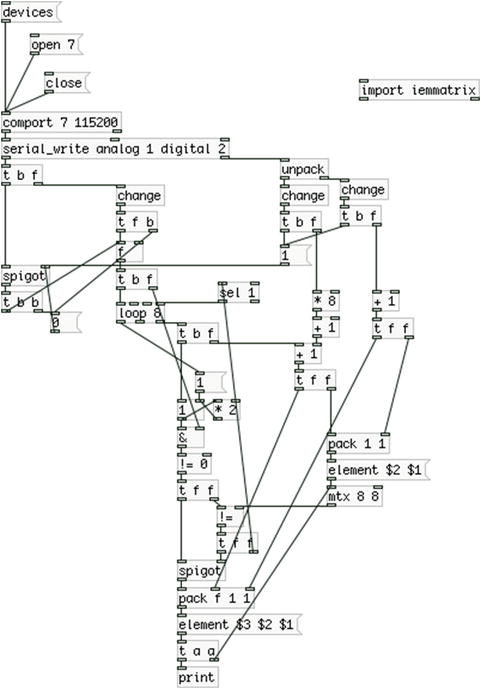
Figure 10-14. Pd patch that reads connection data from the Arduino
Explaining the Pd Patch
In the top part of the patch we make sure the whole process will be executed even if only one of the three bytes changes. I’ll start explaining the last two bytes we’re receiving from the Arduino, since they are being output first (it’s the right to left execution order philosophy of Pd). The input chip is the first of the two values. Since we receive the input as a whole byte, we cannot know which pin in this chip has been connected or disconnected yet. We multiply this value by 8, because the shift registers have eight inputs, and we add 1, because [mtx] starts counting from 1, not 0. Then we store this value to [+ ], which we’ll use later. We initialize the argument of [+ ] to 1, because if we connect to a pin of the first input shift register (which has index 0), the first of these two bytes won’t go through due to [change]. The second value is the output pin. In the Arduino code, we’re iterating through each pin individually, so we do know the exact pin that has changed its connection state. Again, we add 1 because of [mtx] and we send this value to two [pack]s.
Now let’s go to the connection state byte, which is received as an analog value. Once we receive this byte, we store it in [& ] because we’ll need to bitwise AND it the same way we did with the switches of the input shift registers earlier in this chapter. Then we bang [loop 8], which will make a loop of eight iterations, since the pins of a chip are eight. The incrementing value of the loop goes first to the left inlet of [+ ]. We’re adding the input chip number times 8 to retrieve the correct input pin number in every iteration of the loop. For now it’s only one chip, but if we used two, at the first iteration of the loop, the incrementing value would be added to 9, so it would be 9, which would be the first pin of the second chip (again, now we start counting at 1, not 0).
The result of this addition goes to [pack], which already stores the output pin number and outputs this list to the message “element $2 $1”. $2 in this message takes the number of the output pin and $1 the number of the input pin we’re currently querying in our loop. We need to set the output pin as the row of the matrix because of the way an audio matrix we’ll use for the synthesizer works. We’ll see how this functions later on. The message “element” with two values sent to [mtx] queries the value stored in the row and column of the matrix. The output pin number is the row and the input pin number is the column, in the same order we provide arguments to [mtx]. [mtx] will output the value stored at that location to [!= ]. We’ll use this value to check if the stored connection state of the input pin has changed. Remember that the input data is sent as a whole byte, and only here can we tell which pin of an input chip is being connected or disconnected, that’s why we need to make this inequality test.
The Heart of the Patch Mechanism
After we store the connection state of the current input pin, [t b f] that takes input from [loop] bangs a counter which starts from 1 and doubles its value every time. This is the same as raising 2 to an incrementing power starting from 0, but it should be slightly faster than the previous implementation. We prefer this because in the end our patch will be rather busy, so we try to save as much CPU as we can. The next two objects apply exactly the same process with the patch that read the push buttons form the shift registers. It checks if the byte stored in the right inlet of [& ] outputs a 1 or a 0 after it is tested for inequality with 0.
This is the main philosophy of the approach to the patch-bay matrix. A connection between an output and an input pin is perceived as a button press. Since the output pin sends a pulse, while it sends high voltage, the input pin that is connected to it will receive this high voltage, which is the same as having a push button wired to the input pin and pressing it (in this project we’re using pull-down resistors, so button presses are not being inverted). A virtual button press defines a connection between an input and an output pin, and a virtual button release defines a disconnection between the two pins.
Detecting Connections
The connection state that is being detected by [!= 0] is being sent to [!= ] that has stored the previous connection state of the current input pin provided by [mtx] in its right inlet. If the two states are not equal, it means that the connection state has changed and [!= ] will output a 1. This value first goes to [sel 1], which bangs the rightmost inlet of [loop] and stops the loop, and then to the right inlet of [spigot] and opens it. Afterward, the output of [!= 0] goes to the left inlet of [spigot], and since the [spigot] is open, it will go through to [pack f 1 1] (this is also initialized with its second and third arguments to 1). If it’s 0 (meaning that the connection state has not changed) the loop doesn’t stop and [spigot] remains closed.
[pack f 1 1] has stored the output pin number in its right-most inlet and the input pin number in its middle inlet, both initialized to 1. The value it receives in its leftmost inlet is the state of the connection between the two pins it stores in its other two inlets. This connection state will be a 1 if the two pins are being connected and a 0 if they are being disconnected. The output of [pack f 1 1] goes to the message “element $3 $2 $1” which is very similar to the message “element $2 $1”, only it doesn’t query the value of the row and column of the matrix but it sets the last value ($1) to that location. This means that once a connection state has been detected it will be set in [mtx], so when this state changes again it will be detectable. Finally the message “element $3 $2 $1” is being printed to Pd’s console so we can monitor the functionality of the interface. Notice the arguments to [trigger], they are “a a”, which stands for anything. We’re neither passing floats nor symbols, but a whole message. For this reason, we must use [t a a].
Making the Patch-Bay Matrix Circuit
The circuit for the patch-bay matrix is very similar to the combination of the input and output shift register circuits. All pins of the shift registers are wired the same way as before, except from their input and output pins, which were wired to push buttons and LEDs. Now we’re not using buttons or LEDs so these pins are left unwired. We’ll use jumper wires to connect pins of the input and output shift registers in a patch-bay matrix fashion (connections between an output and an input pin are correct, you can’t connect an output to an output or an input to an input). The circuit is shown in Figure 10-15, where the breakout is used for the output and the IC for the input. In this figure, there’s a connection between the output pin 2 (labeled B on the breakout and QB—pin 15—on the IC) and the input pin 5, starting from 1, not 0 (labeled E on the breakout and D4—pin 3—on the IC). This is just to show how the inputs and outputs of the matrix connect to each other. If you make this connection, in Pd, you should get the message “element 2 5 1” printed to the console. Notice that the Clock pin of the breakout board and pin 2 of the IC (the CP pin) are both wired to digital pin 13 of the Arduino, the Serial Clock pin, which synchronizes the transmission of data.
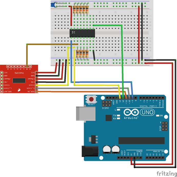
Figure 10-15. A one input and one output shift register patch-bay matrix circuit
This concludes the explanation of the patch-bay matrix. Making such a matrix is no easy or simple task, and we saw that in both the Arduino sketch and the Pd patch. We need to take into account several parameters and we need to keep a log of certain data for the mechanism to work. It might be a bit confusing as to how exactly this patch-bay works. You might need to go through both the Arduino sketch and the Pd patch more than once to really understand their workings. Once you completely understand how they work, you see that the whole approach is based on simple logic blocks that form a complex structure.
To use more inputs and outputs, the only thing we need to do is change the num_of_input_chips and num_of_output_chips constants to the number of chips that we want to use. Then daisy chain the shift registers in the circuit and change the arguments to the [mtx] object, where the first argument is the number of output pins and the second is the number of input pins. These few additions are enough for our matrix to work with any pin configuration. The number of chips used doesn’t have to be the same for input and output, they are independent of each other. The only thing that could bother us is whether we have enough current in our circuit, in case we use too many chips, but we’re not going to reach that limit in this project.
Start Building the Audio Part of the Pd Patch
We can now start building the audio Pd patch for our synthesizer. This will consist of a few different audio modules, which we’ll be able to inter-connect in various ways. Even though the audio software will consist of modules, this is not a modular synthesizer since the hardware will be fixed, and not modular. As with all projects, it’s best to make a rather simple interface that will be easier to achieve. This synthesizer will consist of two oscillators where each oscillator will output all four standard waveforms, one filter with various filter types, and two envelopes which we’ll be able to use either for amplitude, frequency, or any other parameter that can be controlled by a signal.
A Signal Matrix in Pd
The heart of the patch is a matrix. The patch that reads the matrix message, which we’ve already built, is going to be part of our main patch, but that is not the actual matrix that will connect the various audio modules. The iemmatrix library provides another object (among many others in this library) which is a signal matrix. This object is called “mtx_*~”. Figure 10-16 shows a very basic use of it. This object connects its signal inlets with its outlets in a [line~] fashion, making smooth transitions from one state to another. In all matrix messages in this library, the first argument is the number of rows and the second is the number of columns. In [mtx_*~] the rows are translated to outlets and the columns to inlets. The arguments for this object are the number of outlets, the number of inlets, and the ramp time. When trying to create this object you might get an error saying that Pd can’t create it. In this case, type mtx_mul~ instead.
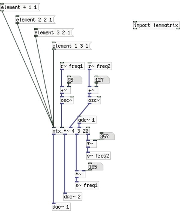
Figure 10-16. A basic use of [mtx_*~]
In Figure 10-16, the second argument is 3, but we get five inlets. This is because the first inlet takes only matrix messages, and the last one (which is a control inlet) overrides the last argument, the ramp time. A matrix message of the form “element 3 2 1” means, “multiply the input of inlet 2 by 1 and connect it to outlet 3.” Again, the first number of the message is the row/outlet number of the matrix, the second is the column/inlet of the matrix, and the third is the value to write to that position of the matrix. In [mtx_*~] a value at a certain position means a multiplication by that value of the column/inlet, connected to the row/outlet.
In Figure 10-16, we’re connecting the output of the first oscillator to the frequency input of the second (with the message “element 4 1 1”). This is followed by the output of the second oscillator to the right speaker of the computer, and then the output of the second oscillator to the frequency input of the first oscillator, and lastly the input of the computer’s microphone to the left speaker. Using the messages generated by the patch that reads the patch-bay matrix from the Arduino, we can make connections dynamically according to the physical connections of the patch-bay matrix.
Here we are presented to a basic concept of the patch-bay matrix, which is a sort of a caveat. The outlets of the oscillators are connected to inlets of the matrix, and the outlets of the matrix sometimes end up in inlets of the oscillators. This might seem a bit obvious, but what we really need to get used to is that the inlets of the hardware interface will actually be outlets for the software, and vice versa. So from now on, you should bear in mind that the output shift registers will play the role of inputs and the input shift registers will play the role of outputs.
Building the Modules for the Synthesizer
Since the audio software in this project is modular, we can build these modules as abstractions and then load them in the main patch. We’ll first build the two oscillator modules, where one will be a non-band limited and the other will be a band-limited oscillator (a table lookup oscillator with waveforms built with the sinesum feature of Pd). We’ll start with the non-band limited one.
The First Module, a Non-Band Limited Oscillator
Figure 10-17 shows the first module abstraction, which is called “all_osc~”, because it outputs all four standard oscillator waveforms. It is not a very complex abstraction, but it’s not very simple either. Let’s start looking at its subpatches.
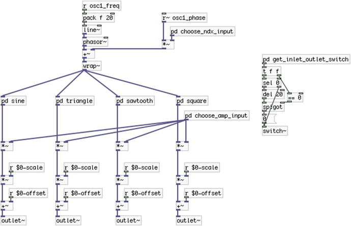
Figure 10-17. Contents of the all_osc~ abstraction
The get_inlet_outlet_switch Subpatch
The first subpatch we should look at is the [pd get_inlet_outlet_switch], which is shown in Figure 10-18. This subpatch deploys a basic concept in this project, which is taking advantage of connections of modules to control their DSP. On the left part of the patch we receive a message with [r mtx_msg], which stands for matrix message. This message is always of the type element $1 $2 $3. What we care about is whether an outlet in this module is connected to the matrix. If it is, it means that we are using this module so we should turn its DSP on. Remember that a module’s outlet is a matrix’s inlet.
Since this is an abstraction, we’ll provide two arguments, the first inlet of the matrix it connects to, and the first outlet of the matrix it receives input from. These arguments are being passed to the abstraction from the bottom part of the subpatch in Figure 10-18. At the left part of the subpatch, we split the matrix message to two, where the second half will be the matrix inlet number and the connection state. We first store the connection state to [f ], and then we check if the inlet of the matrix message is one of the outlets of this abstraction, which are four in total. If it is, we pass the connection state through the [spigot] and we scale it and give it an offset so that a 1 will be 1 and a 0 will be –1. This way, we can accumulate these values, because we might connect more than one of the module’s outlets to the matrix, so we need to know when all its outlets will be disconnected, so we can turn its DSP off. We use [clip 0 100] to make sure we won’t go below 0 (we’ll never reach 100 connections, it’s there just to give some headroom for the clipping).
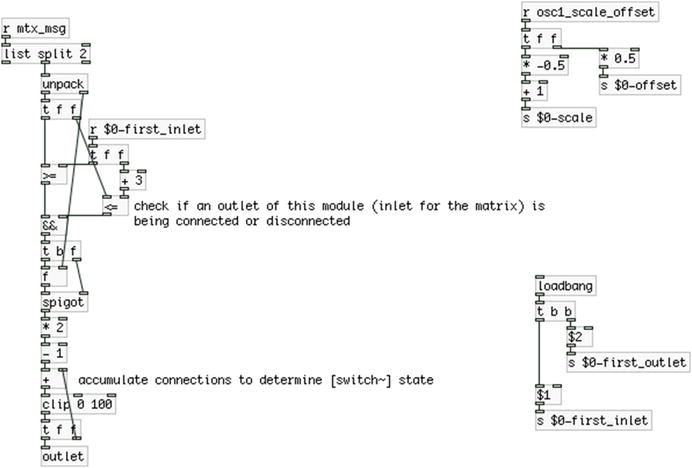
Figure 10-18. Contents of the get_inlet_outlet_switch subpatch
In the parent patch of the abstraction, shown in Figure 10-17, we can see that when the subpatch in Figure 10-18 outputs a 0, we delay it by 20 milliseconds, because this is the ramp time of [mtx_*~]. This way, we will avoid clicks when we turn the DSP of the subpatch off. We reverse the value to control a [spigot] because as we connect or disconnect a patch cord, the connection will wobble a few times (this will take a couple of milliseconds, if not microseconds). This wobbling might result in a sequence of 1s and 0s when we connect the patch cord, ending in 1. A 0 will delay its output by 20 milliseconds, so the last 0 before the last 1 will give its output after the last 1, resulting in turning the DSP of the abstraction off. Using a [spigot] this way prevents this from happening.
At the top-right side of the patch we will be receiving the values of a switch which we’ll use to scale and offset the output of all four waveforms, so that we can either have the oscillator’s full amplitude, or reduce it to a range from 0 to 1. We’ll add this switch when we build the final circuit for this project because we may want to control the amplitude of the other oscillator, or its index, and we don’t want negative values. In the parent patch of the abstraction we can see the corresponding [receive]s of these [send]s, at the output of each waveform.
The next subpatch we’ll look at is [pd choose_ndx_input], which is shown in Figure 10-19. In this subpatch, we set the control of the phase modulation index of the oscillator. Again, we’re using the matrix messages to determine whether we connect a signal to the specific inlet of the module, so this time we query the outlet of the matrix message, that’s why the implementation is slightly different than that in Figure 10-18. We add 1 to the outlet number because the first inlet of the module (outlet of the matrix) will be the signal that will modulate the phase of this oscillator.
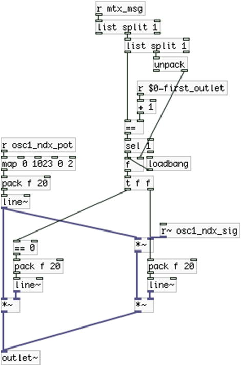
Figure 10-19. Contents of the choose_ndx_input subpatch
Because of the right-to-left execution order in Pd, the connection state will be output first out of [unpack] and the rest of the values afterward. What we do here is store the state value and query the matrix outlet number. If this number fits the matrix outlet number connected to [s~ osc1_ndx_sig], we output the connection state to determine whether a signal is connected to that outlet or not. We need to bang the connection state only when the outlet number of the matrix message fits the outlet we want to query; otherwise, we would be controlling this subpatch with any connection we made in the patch-bay matrix, and we don’t want that.
Note that we don’t really need to accumulate connections since we’ll most likely have only one signal connected to this inlet. If there is a signal connected to this inlet, we’ll choose that, if there’s no signal connected, we’ll choose the values we’ll be receiving from a potentiometer, received with [r osc1_ndx_pot]. The value of this potentiometer will also control the amplitude of the input signal, because we might want to have a different range for the index than that of the input signal.
Since we need to determine which signal will control the index from the moment we’ll open the patch, we bang [f ] on load, which will hold 0 by default. This means that by default we choose the potentiometer values to control the index, and only if we connect a signal to the matrix outlet connected to [s~ osc1_ndx_sig] will we set that signal to control it.
This subpatch is almost identical to [pd choose_ndx_input]. The only things that change are the names of the [receive]s that receive the potentiometer value and signal, the mapping of the potentiometer values, and the number of the matrix outlet. It is shown in Figure 10-20. There’s no real need to explain it, because I’ve already explained [pd choose_ndx_input]. Only note that we’re adding 2 to [r $0-first_outlet], since this signal will arrive at the third inlet of the module.
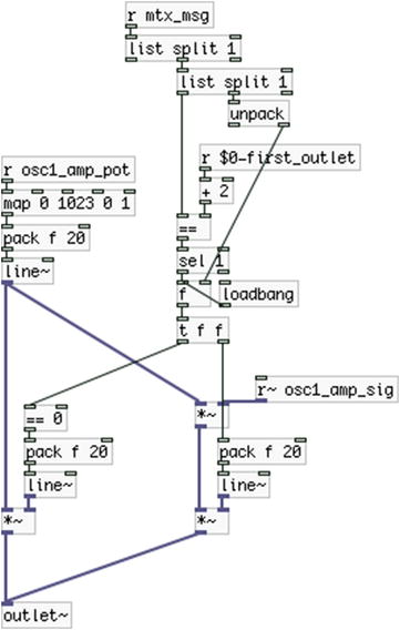
Figure 10-20. Contents of the choose_amp_input subpatch
The last thing we need to look at is the subpatches of the four waveforms. We have already seen these waveforms a few times in this book, but here we add the connection feature that controls the DSP of a patch. They are shown in Figure 10-21 through 10-24. This time we care about whether the outlet of each subpatch is connected to the matrix, so we filter the matrix message to get the matrix inlet number and the connection state. Again, if the subpatch gets disconnected from the matrix we delay zeroing the subpatch by 20 milliseconds to avoid clicks because of the 20 millisecond ramp of [mtx_*~]. Each subpatch is controlled by a different outlet of the module, where the sine wave subpatch is controlled by the first outlet, and the next ones are controlled by the successive outlets. Notice that [pd square] receives a value in [r duty_cycle], which will be sent by a potentiometer in the final circuit.
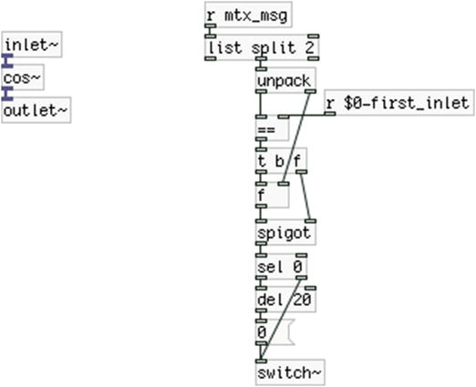
Figure 10-21. Contents of the sine subpatch
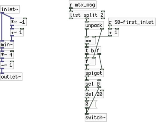
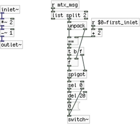
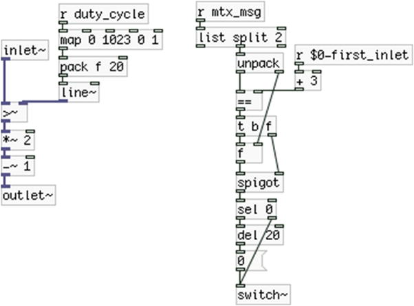
Figure 10-24. Contents of the square subpatch
Controlling the DSP of each of these subpatches separately, and of the parent patch as well, will save some CPU when this module won’t be used. Eventually we want to use this patch with an embedded computer and CPU is always something to consider, as these computers are not as powerful as a personal computer. This project won’t have that many modules, and it’s very likely that all will often be playing simultaneously. Nevertheless, knowing how to utilize this feature will prove very helpful as a project grows.
The Second Module, a Band-Limited Oscillator
The second module is very similar to the first and it is called “bl_all_osc~”. There are small differences and these are the ones we’ll deal with. Whatever is not shown here is identical to the first module. The parent patch of the abstraction is shown in Figure 10-25. In the center of the patch we have the [phasor~], which drives the four table lookup oscillators. After we modulate its phase, we [wrap~] it around 0 and 1 to make sure we’ll always stay within the bounds of the waveform tables and we multiply this output by the size of the tables and add 1, because the tables add the three guard-points with the sinesum feature. We’ve added some mapping to the frequency potentiometer values to get very low frequencies, which we might want to use in combination with the envelope module we’ll build later. Of course, it’s only a suggestion.
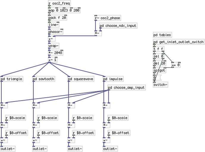
Figure 10-25. The bl_all_osc~ abstraction
Apart from that, the main difference is that all [receive]s have their names changed to osc2. So, wherever you have a [receive] make sure you apply this change (the rest of the name stays the same, as with [r~ osc2_freq]). These [receive]s are in [pd choose_ndx_input, [pd choose_amp_input], in [pd get_inlet_outlet_switch] and in the four subpatches that read the stored waveforms. We also have an additional subpatch that creates the waveform tables, which is shown in Figure 10-26.
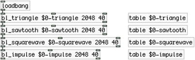
Figure 10-26. Contents of the tables subpatch
We’ve seen this subpatch again in this book, but we’re showing it here too, because it is a more minimal version. We’re using the abstractions that create band-limited waveforms, which we have used Chapter 8, so the waveforms are being created when the patch opens. There’s nothing special here, only that.
Since the waveforms are stored in tables, the subpatches that read them are identical, except from the name of the table they’re reading from and the number of the matrix inlet they query. [pd triangle] is shown in Figure 10-27. There’s no need to show the other three; you can build them yourself. Only take care to change the name of the table [tabread4~] reads from, and put a [+ ] below [r $0-first_inlet], where the argument to [+ ] will be incrementing, being 1 for [pd sawtooth], 2 for [pd squarewave], and 3 for [pd impulse].
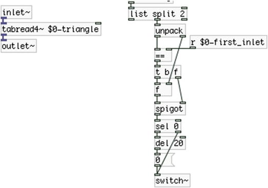
Figure 10-27. Contents of the triangle subpatch
This module doesn’t have a sine waveform since there’s no difference between a sine created by a [phasor~] and [cos~] and a sine created with sinesum. If you check the source code of [cos~] you’ll see that it reads from a table where a cosine waveform is stored, which is essentially the same thing a [tabread4~] would do with a sine waveform created with sinesum. We’ve replaced the sine wave with an impulse waveform.
Third Module, a Multiple Type Filter
Our third module is simpler than the first two. We’ll use a filter abstraction I’ve made with which we can have multiple filter types at the same time. This abstraction is [multiFilter_abs~] and you can find it on GitHub, in the same repository with [omniFilter_abs~], used in Chapter 5 (most likely you’ve already downloaded it if you built the project in Chapter 5). The module is shown in Figure 10-28. Name it multi_filter~. [multiFilter_abs~] gives eight outputs (for now, they might grow in the future) of which we’ll use three. This is because we need to bear in mind how many inputs and outputs our synthesizer will have.
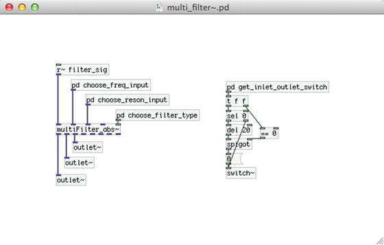
Figure 10-28. The multi_filter~ module abstraction
We have already built two modules both of which have three inputs and four outputs. Since the inputs and outputs are inverted because of the matrix, we are already occupying eight pins of the inputs shift registers (that makes an entire chip) and six pin of the output shift registers. The filter module takes another three inputs and three outputs, making a total of eleven pin of the input shift registers and nine pins of the output ones. We’ll be using two chips of each shift registers, so we’ll have 16 pins of each available. What’ we’re left with is five inputs and seven outputs. We’ll need another two outputs for the [dac~], and two inputs and two outputs for the last module, which will be two separate envelopes. We also need to have three switches (one for each oscillator module and one for the DAC) and if possible, as many LEDs. If you think about it, we have already occupied all pins of all chips, so when building such an instrument we need to be careful as to what each module will do.
We’re not going to show the contents of [pd choose_freq_input] and [pd choose_reson_input], because they are almost identical to the similar ones of the previous modules. Just make sure you change the names of the [receive] objects to [r filt_freq_pot] and [r~ filt_freq_sig] for [pd choose_freq_input] and [r filt_reson_pot] and [r~ filt_reson_sig] for the [pd choose_reson_input] (“reson” stands for resonance). Also, in [pd choose_freq_input] map the value of [r filt_freq_pot] to a range from 20 to 10,000 and put have a [+ 1] under [r $0-first_outlet] and in [pd choose_reson_input] map the value to a range from 0 to 1 and put a [+ 2].
The choose_filter_type Subpatch
Figure 10-29 shows the contents of [pd choose_filter_type]. The data we need is the connection state of the [outlet~]s of the abstraction, so we must use the inlet number of the matrix message along with the connection state. We’re filtering the matrix message to isolate these two values. Then we subtract the number of the first matrix inlet this abstraction will be connected to. This way, the matrix inlet numbers of this abstraction will start from 0. We send the offset matrix inlet number along with the connection state to [route 0 1 2], which will set the [switch~] state of each filter type accordingly. [multiFilter_abs~] takes messages of the type lowpass 1 or lowpass 0 to turn the DSP of the lowpass filter on or off. Check its help patch for more information.
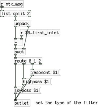
Figure 10-29. Contents of the choose_filter_type subpatch
The way that this subpatch works, as soon as we connect one of the abstraction’s [outlet~]s to the matrix, [multiFilter_abs~] will receive the appropriate message and will turn on the DSP of the corresponding filter inside it. When we disconnect the [outlet~], it will receive the appropriate message to turn that DSP off. This way, we can save a lot of CPU, since filters can be CPU-intensive.
The get_inlet_outlet_switch Subpatch
This subpatch is nearly the same as the other two modules we’ve built, that’s why we’re showing it here. It is shown in Figure 10-30. The differences are that we don’t have a switch to scale and offset the output signal of the module, and that we have three [outlet~]s in total. Thus we have a [+ 2] below [r $0-first_inlet], so we can check that the matrix inlets we get from the matrix messages correspond to the [outlet~]s in this module. Apart from that, it is the same as the corresponding subpatches in the previous two modules that we built.
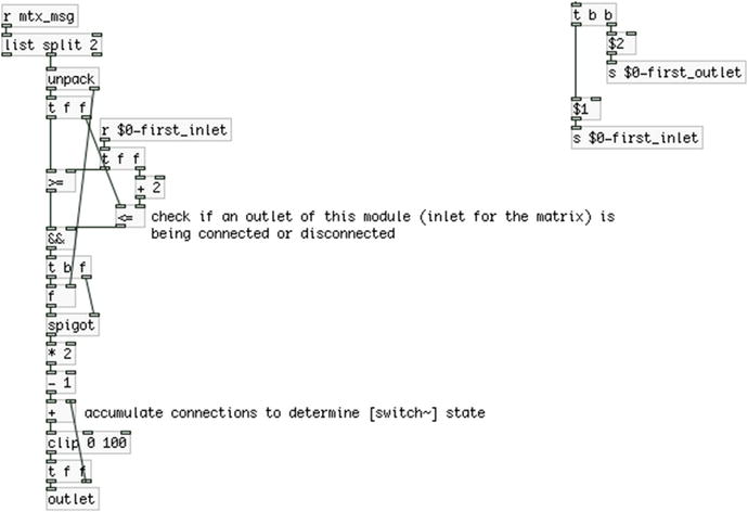
Figure 10-30. Contents of the get_inlet_outlet_switch subpatch
The Fourth Module, Two Envelopes
The last module that we’ll build for our synthesizer is an envelope module, which we can use to control various parameters of the other modules. Its name is “envelope~” and you can see it in Figure 10-31. Its parent patch is very simple, but we’ll need to take a look at its subpatches.
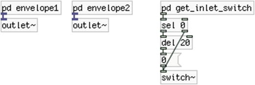
Figure 10-31. The envelope~ module abstraction
The contents of [pd envelope1] are shown in Figure 10-32. On the right side we have the connection control for the [switch~] of the subpatch, like with all other subpatches of the other modules. The heart of this subpatch is [ggee/envge], which we’re using for the envelope. Its arguments are “100 60” to be rather small so that it doesn’t take too much space in the patch. Above it we have an object we haven’t seen before, [threshold~]. This object outputs a bang out its left outlet when the signal in its left inlet rises above the value of its first argument (the trigger threshold). It also outputs a bang out its right outlet when the same signal goes below the value of its third argument (the rest threshold). The second and fourth arguments are the debounce time set in milliseconds, within which [threshold~] won’t output a bang if the signal exceeds the trigger and rest thresholds. Using this object enables us to use an oscillator to control the triggering of the envelopes, so that we don’t need to do this manually. This is a desired feature in many cases, and you can build interesting rhythms this way. Notice that we’re using both outlets of [threshold~] to trigger the envelope and since we have separate control on the trigger and rest thresholds, we can have a rather big variety in the possible rhythms we can produce.
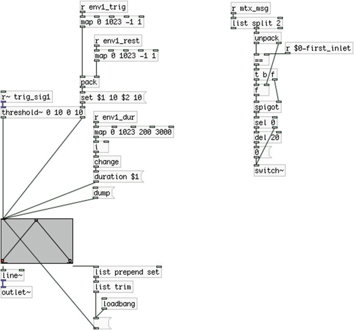
Figure 10-32. Contents of the envelope1 subpatch
In this subpatch, we receive three potentiometer values. The first one controls the trigger threshold value and the second controls the rest threshold value. We can set these values with the message “set $1 10 $2 10”, which will override the arguments of the object. This value can be between –1 and 1, since the oscillators of the synthesizer will control the triggering of the envelopes. The third potentiometer will control the duration of the envelope, as we’ve seen before (in Chapter 4).
As in Chapter 4, create the envelope you want and click the “dump” message. [ggee/envgen] will output the breakpoint values and positions out its right outlet and we’ll save them in a message, which will be banged when the patch opens. This way, we can save our envelopes.
[pd envelope2] is identical to [pd envelope1]. Only the names of the [receive]s change their numbering from 1 to 2, and a [+ 1] should go below [r $0-first_inlet].
There is a small difference in the [pd get_inlet_switch] subpatch of this abstraction and the [pd get_inlet_outlet_switch] of the other abstractions. The subpatch name says it, we don’t need to know the matrix outlet number this module will take input from, so we’re excluding it. The subpatch is shown in Figure 10-33.
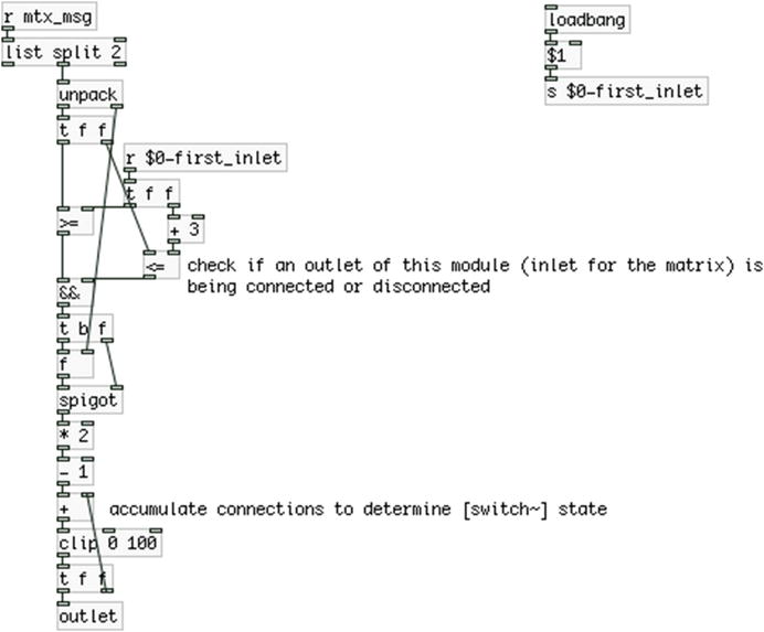
Figure 10-33. Contents of the get_inlet_switch subpatch
The Final Patch
Now that we’ve built the four module we’ll use in this project it’s time to build the final patch. It is shown in Figure 10-34. We have ended up with a matrix with 13 rows/outlets and 13 columns/inlets. There’s not need to have the same amount of rows and columns, it just happened the way we built the interface. They are completely independent of each other, so if you want to build something different, don’t worry about this relationship.
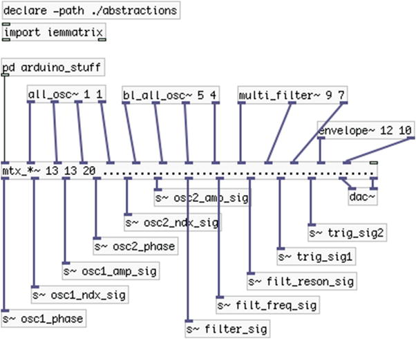
Figure 10-34. The final patch
We can see the four abstractions we’ve built with the matrix inlet they connect to as their first argument, and the matrix outlet the first [s~ ] that sends signal to them is connected to as their second argument. Of course, we need to place a [dac~] somewhere otherwise we wouldn’t have any sound. There’ only one subpatch that we need to look at, which is [pd arduino_stuff]. The rest should all be clear. Just note that all the module abstractions we’ve built have been placed in a directory called abstractions inside the directory of this patch, the path of which we add with [declare].
Figure 10-35 shows [pd arduino_stuff]. We’re using the [serial_write] abstraction, but this time we provide five arguments to it. The fifth argument is the first character of the data stream from the Arduino. We choose a different one from 192 that we’ve been using so far, for a reason that will be explained when we go through the [pd get_switches] subpatch inside this subpatch. We’re also using a different baud rate (57,600) because the 115,200 is probably too fast for the Arduino to handle. You can try for yourselves. There are three subpatches in total in [pd arduino_stuff], which we need to explain.
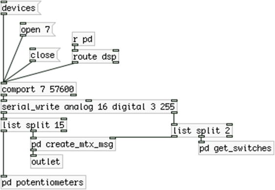
Figure 10-35. Contents of the arduino_stuff subpatch
The only thing we might need to explain here is that we’ll be using fifteen potentiometers in total, and the connection state byte split in two. Then we’ll receive the connected input chip, the connected output pin, and finally a byte that will hold the states of the three switches of our circuit (one for the scaling of each oscillator and one for turning on the DSP). This should clarify the arguments passed to [serial_write].
There’s nothing special about this subpatch. It’s shown in Figure 10-36. We’re just diffusing of the potentiometers of our circuit to their destinations.
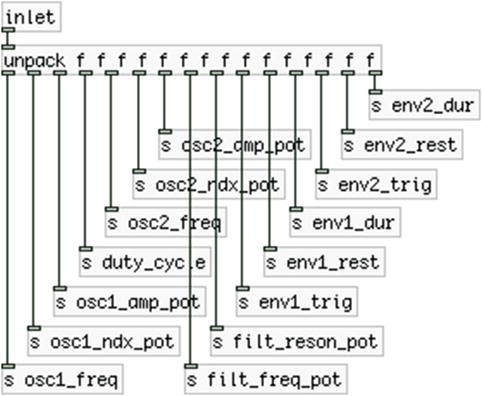
Figure 10-36. Contents of the potentiometers subpatch
In this subpatch, we’re creating the matrix messages according to the input we get from the Arduino. It is shown in Figure 10-37. Essentially, it’s the same as the first patch that we used with the first patch-bay matrix we built in this chapter. The only two differences are that since we have only 13 matrix inputs, we’re not using the last three pins of the second input shift register, that’s why we use the input chip number we receive from the left outlet of [unpack] to determine how many iterations our loop will do. If we omit that and iterate eight times for both chips, we’ll go through the three switches our circuit will have, since they will be wired to the second input shift register, and that will create unexpected behavior.
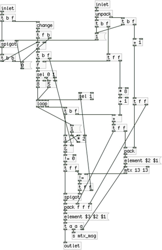
Figure 10-37. Contents of the create_mtx_msg subpatch
The other difference is that apart from updating [mtx] (which, by the way, now has 13 rows and 13 columns, as many as [mtx_*~] in the parent patch) and sending the matrix message to the [outlet] (instead of [print]), we also send it to [s mtx_msg], which is received in every module. So we can use the matrix messages to control the DSP of each module and its subpatches.
The last subpatch we need to check is [pd get_switches], which is shown in Figure 10-38. In this subpatch, we’ll receive a single byte that will hold the states of the three switches that will be wired to the second input shift register. These switches will be wired to the chip’s pins 5, 6, and 7. For this reason, the loop we’ll run to determine the state of each one must iterate through these three numbers only. The rest of the process has been explained earlier in this chapter when we were reading switches with the input shift registers.
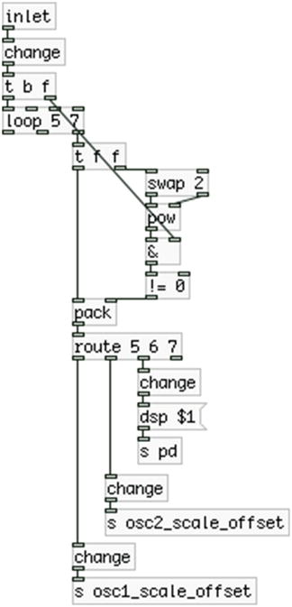
Figure 10-38. Contents of the get_switches subpatch
The first of these switches will control the scaling and offset of the first oscillator. The second switch will control the scaling and offset of the second oscillator. The last switch will control the DSP of Pd. In Figure 10-35 we can see a [r pd] connected to [route dsp], like we’ve used it in some other chapters already. That value will control an LED of our circuit so we can have visual feedback for when the DSP is on.
Let’s come back to the [pd arduino_stuff] subpatch shown in Figure 10-35. Since we’re receiving the states of all three switches in one single byte, and because this byte will have its most significant bit (the rightmost bit) set to 1, when the third switch is in the on position (these switches are wired to the last three pins of the second input shift register), this byte will potentially get the same value as our start character. To be precise, we need to test which decimal values the eight possible combinations of the three switches can get, and determine whether it is indeed possible that one of these combinations will be 192. Instead of going through this process, we can just change the start character simply by providing a fifth argument to the [serial_write] abstraction, and by setting the same value in the definition of the data transfer array in the Arduino code. We’ll be masking this byte with all other bits set to 0 in the Arduino code, so there’s no way it will ever reach 255. We’ll see it in detail when we go through the Arduino sketch.
This concludes the Pd patch, so now we can move on to the final version of the Arduino code.
The Final Arduino Code
Listing 10-8 shows the final code that works with the final Pd patch. We’ve already seen most of the stuff, but there are a few additions that are project-specific, such as the switches and LEDs attached to the shift registers and that we can read them independently from the patch-bay matrix inputs and outputs.
In line 9, we define an array called num_of_pots. We’ll use that in the main loop function to iterate only through the fifteen pins of the multiplexer. Even though this array has only one element, it’s good to define this variable as an array in case we want to use more multiplexer chips. In line 10, we still define the num_of_mux_channels so that we can use the preprocessor directive LOG2 to get the num_ctl_pins in line 11.
Line 31 defines a variable that holds the pin number of the last input shift register where the first switch of our circuit is attached to (this switch will control the scaling and offset of the first oscillator). Then in line 33, we define the pin number of the last output shift register where the DSP LED will be attached to (it’s the last pin of the chip). In line 35, we define the first pin the first LED of our circuit will be attached to on the last output shift register. In line 37, we define how many switches in our circuit will control LEDs without having data from the serial line intervening. In line 49, we define the transfer_array with its first byte initialized to 255, like we did in the Pd patch.
Using Binary Numbers for Masking
We jumped line 39 deliberately, because we need to explain it separately. In this line we define a binary number, hence the capital B in the beginning of it. This way, we can define binary numbers in the Arduino language. This number represents the pins of the last input shift register where the three switches are attached to. These are the last three pins, that’s why the first three digits of this number are 1s and the rest are 0s. Shift registers map their bytes this way, the Least Significant Bit (referred to as LSB, it’s the rightmost digit) represents the state of the first pin, and the Most Significant Bit (referred to as MSB, it’s the leftmost digit) represents the state of the last pin.
We’ll need this value to mask the last byte of the input_bytes array. If we don’t mask it, and we change the position of a switch but we don’t make a new connection, this byte will change and the test we make in the check_connections function to see whether we have a change in the input_bytes array will succeed, even if no new connection has occurred. This will result in storing this byte to the transfer_array. Consequently, it will trigger the loop that detects connections in Pd, as shown in Figure 10-33. Anyway, in Pd, we only go through the connection pins, so the patch wouldn’t try to make a new connection, but the loop would be triggered. Masking this byte will prevent this loop from being triggered, because we use [change], and the positions of the switches won’t affect this last byte at all.
Using a binary value instead of a decimal is very convenient in such cases because we don’t need to really think arithmetically. With such a number, we can clearly represent our circuit, since we can just use 1s for the chip pins we’re interested and 0s for the pins we don’t need.
The check_connections Function
We’ve introduced a small modification in the check_connections function. What we do is copy the byte of the input_bytes array because if we’re iterating through its last byte, we need to mask it with the binary reversed value the switch_mask variable hold. We reverse this value by using the tilde character (~). This is another bitwise operation that swaps the bits of a value, replacing all 1s with 0s and vice versa. The switch_mask variable has 1s in the bits of the switches, but we need to mask the last byte of the input_bytes array the other way round, having 1s in the bits of the connection pins.
If we don’t copy this byte, we’ll modify it and we won’t be able to detect the switch positions anymore, as the bits of the switches will have 0s no matter what we do with them. We could have stored a binary value with the switch pins set to 0, but I found it a bit more intuitive to set these pins to 1, as it makes it clearer that we need to isolate them.
The Main loop Function
In the main loop function, the first thing we do is check if we’ve received data from the serial line. This will happen only when we turn the DSP on in Pd. If we do receive data, we’ll set the state of the DSP LED using the bitWrite function. This function is very similar to the bitSet and bitClear functions we’ve already used, but it takes three arguments, the byte to write to one of its bits to, the bit of the byte, and the value to write to that bit. The DSP LED is wired to the last output shift register, so we use the last byte of the output_bytes array. The bit of that byte is set by the dsp_led variable, and the value of that bit is set by the byte we receive from the serial line.
After that, we go on and read the fifteen potentiometers of our circuit, and then we check if we have a new connection in the patch-bay matrix. In line 154, we store the last byte of the input_bytes array to the transfer_array. We’ll use that byte to retrieve the states of the three switches of our circuit. For this reason we mask it with the switch_mask variable, this time without inverting it (so defining it this way and not inverted was not without a reason after all). Again, this is not really necessary, but it will prevent the loop that detects the switch states from being triggered, saving some little CPU in Pd. We’ve already seen how we detect the switch states when I explained the [pd get_switches] subpatch inside the [pd arduino_stuff] subpatch of the final Pd patch.
Controlling the LEDs with the Switches of the Shift Registers
In lines 158 and 159, we make copies of the first_switch and first_led variables, because we want to post-increment them. If we used these variables immediately, we would change their values and after the first iteration of the loop function, they would already be beyond the bounds of the shift register pins. In line 160, we run a loop for the two switches that control their LEDs without serial data intervening. This time we use a combination of the bitRead and the bitWrite function to read each switch value and write it to its LED. The former is similar to the latter, only it takes two arguments instead of three: the byte to read a bit from and the bit of the byte to read. It shouldn’t be too hard to understand how this loop works. Finally, we write the transfer_array to serial line. This concludes the Arduino code for this project.
The Final Circuit
You’ll probably know how to build the circuit already, but it is shown here anyway. Figure 10-39 illustrates it with breakouts for the multiplexer and the output shift registers (refer to previous sections of this chapter for wiring the ICs). The potentiometers are not included in the circuit because it would become rather messy. You should know how to wire them by now. The three switches wired to the last three pins of the second input shift register and the three LEDs wired to the last three pins of the second output shift register are included. Take care to connect one pin of the switch to the voltage (if it’s an ON/ON switch, this should be the middle pin). You can now test your circuit with the Pd patch, you’ve made a patch-bay matrix synthesizer!
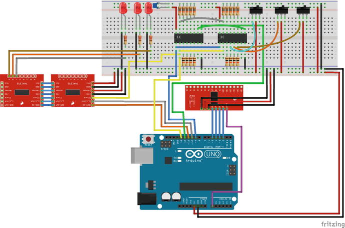
Figure 10-39. The final circuit
Making an Enclosure
We’ve already made a few enclosures in this book, but with this one, there are a few tips and tricks that you might find helpful. First, since this project is highly customizable, you could argue if the setup of the hardware interface should be project specific, or if it should be more generic so that it can host other implementations of the software. This means that you should decide where to place all the components on the enclosure. Having all the female banana terminals placed according to the connections of the software they represent, and the potentiometers grouped according to the modules of the software they control is very helpful for the specific project, but limits the hardware interface to this project’s software. On the other hand, making a generic layout can be a bit confusing, as you should remember what each component is for, and the layout won’t help in telling that. Figure 10-40 shows my approach to the hardware layout of the patch-bay matrix and the other components. This figure includes some connections between banana terminals to show how they are to be connected. As you can see, I chose to have the patch-bay in the middle so I can use the same enclosure for another type of synthesizer. This way, I’m not limited to the software built in this chapter. I’ve also used 16 potentiometers instead of 15 to have as many as the multiplexer provides in case I want to use this enclosure for another project. It’s up to you which route you’ll take in designing this.
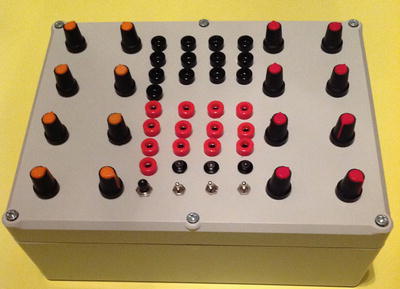
Figure 10-40. A patch-bay matrix synthesizer layout
Another thing you might want to have is access to the Ethernet, in case you embed a computer in the enclosure. A good idea is to use an Ethernet gender changer (this is actually a female-to-female Ethernet port) and a flexible Ethernet cable, so you can connect your embedded computer’s Ethernet to the gender changer, which on its other side is a female Ethernet, thus giving you access to the port of the embedded computer.
Lastly, concerning the banana terminals, it is a good idea to use different colors for different purposes. In Figure 10-40, I’ve used black bananas for input (matrix and shift register output) and red for output (matrix and shift register input). You might want to use a third color for control signal inlets (the phase inlet of the oscillators, for example), especially if you make your layout based on the specific project. All the female banana terminals are wired to the free pins of the input and output shift registers, which are pins A to H on the breakouts and D0 to D7 on the input IC and QA to QH on the output IC. By free I mean all these pins that are not wired to switches or LEDs (refer to Figure 10-39). Using cables with male banana terminals enables us to make connections between input and output pins, much like we did with the jumper wires on the breadboard version of this project.
You also might want to include a diode in each patch cord. Banana terminals can be stacked so that you can connect more than one patch cord to a female banana. Using diodes in the patch cords will prevent the current flowing from one patch cord to another in case of stacked bananas. In Figure 10-40, if no diodes were included in the patch cords, output pin 9, which is connected to input pin 7, would seem like it’s also connected to input pin 1. That’s because while the output pin 9 would be HIGH, its current would flow through the cable of the patch cord to input pin 7. But that input pin has two banana terminals stacked. This would result in the current flowing further to output pin 7 and from there to input pin 1. Try to follow the connections in Figure 10-40 and you’ll understand. The white patches in the cables include diodes, which prevent the current flowing from an input to an output. The ring of the diode is oriented toward the black banana terminal, which connects to the output shift registers.
Shutting down the Embedded Computer
As you can see in Figure 10-40, I’ve included an additional push button (on the right side of the three switches). I’m using this to shut down the embedded computer, like we’ve done in previous chapters. This push button is connected to one of the free digital pins of the Arduino, using the internal pull-up resistor. (This means that in the circuit, its one leg should connect to the Arduino digital pin, and the other to ground.) I suggest that you read this switch at the end of all data (this means that you must modify the array index the three switch byte is stored at), using the exclamation mark to reverse its value (remember, the pull-up resistor reads HIGH when the button is not pressed).
As always, you need to write a script to kill Pd and shut the embedded computer down, which you can call with [shell]. I’m using the DSP switch to control whether this button’s values go through or not, so that I can’t accidentally shut down the computer while the DSP is running. Figure 10-41 shows the addition to the [pd get_switches] subpatch. The rest are left for you to implement yourself, as you should be pretty familiar with the process by now. Note that you’ll have to change the fourth argument to [serial_write], since it will now receive 4 bytes as “digital” values.
Figure 10-41. Addition to the get_switches subpatch to shut the embedded computer down
Conclusion
We have built a rather complex instrument that comprises many levels, in both the software and the hardware. You have been introduced to techniques and devices that expand the capabilities of the Arduino. You’ve seen that you can use very simple principles, like setting a digital pin HIGH or LOW, read these voltages from another digital pin, and create a much more complex interface.
This last project was probably the most difficult of all the projects in this book. Still, the programming level increased chapter by chapter, so by reaching this chapter, you should now have the understanding and tools to follow the process of making an instrument. You have seen a lot of different techniques and approaches to making musical interfaces. Now you should be able to create your own projects, solve problems, and come up with original ideas in both the technical and the creative processes.