
The Serial Peripheral Interface bus, known affectionately as spy, is a synchronous serial interface that was named by Motorola.18 The SPI protocol operates in full-duplex mode, allowing it to send and receive data simultaneously. Generally speaking, SPI has a speed advantage over the I2C protocol but requires more connections.
SPI Basics
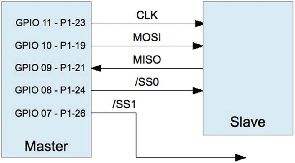
SPI interface
Data is transmitted from the master to the slave by using the MOSI line (master out, slave in). As each bit is being sent out by the master, the slave simultaneously sends data on the MISO line (master in, slave out). Bits are shifted out of the master and into the slave, while bits are shifted out of the slave and into the master. Both transfers occur to the beat of the system clock (CLK).
Many SPI devices support only 8-bit transfers, while others are more flexible. The SPI bus is a de facto standard, meaning that there is no standard for data transfer width and SPI mode.18 The SPI controller can also be configured to transmit the most significant or the least significant bit first. All of this flexibility can result in confusion.
SPI Mode
Parameter | Description |
|---|---|
CPOL | Clock polarity |
CPHA | Clock phase |
SPI Modes
CPOL | CPHA | Mode | Description | |
|---|---|---|---|---|
0 | 0 | 0,0 | 0 | Noninverted clock, sampled on rising edge |
0 | 1 | 0,1 | 1 | Noninverted clock, sampled on falling edge |
1 | 0 | 1,0 | 2 | Inverted clock, sampled on rising edge |
1 | 1 | 1,1 | 3 | Inverted clock, sampled on falling edge |
Clock Sense | Description | |||
Noninverted | Signal is idle low, active high | |||
Inverted | Signal is idle high, active low | |||
Peripheral manufacturers did not define a standard signaling convention in the beginning. Consequently SPI controllers often allow configuration of any of the four modes while the remaining only permit two of the modes. However, once a mode has been chosen, all slaves on the same bus must agree.
Signaling
 (slave select) active. Only one slave can be selected at a time, since there must be one slave driving the MISO line. Shortly after the slave is selected, the master drives the MOSI line, and the slave simultaneously drives the MISO line with the first data bit. This can be the most or least significant bit, depending on how the controller is configured. The diagram shows the least significant bit first.
SPI signaling, modes 0 and 2
In mode 0,0 the first bit is clocked into the master and slave when the clock line falls from high to low. This clock transition is positioned midway in the data bit cell. The remaining bits are successively clocked into master and slave simultaneously as the clock transitions from high to low. The transmission ends when the master deactivates the slave select line. When the clock polarity is reversed (CPOL = 1, CPHA = 0), the clock signal shown in Figure 16-2 is simply inverted. The data is clocked at the same time in the data cell, but on the rising edge of the clock instead.
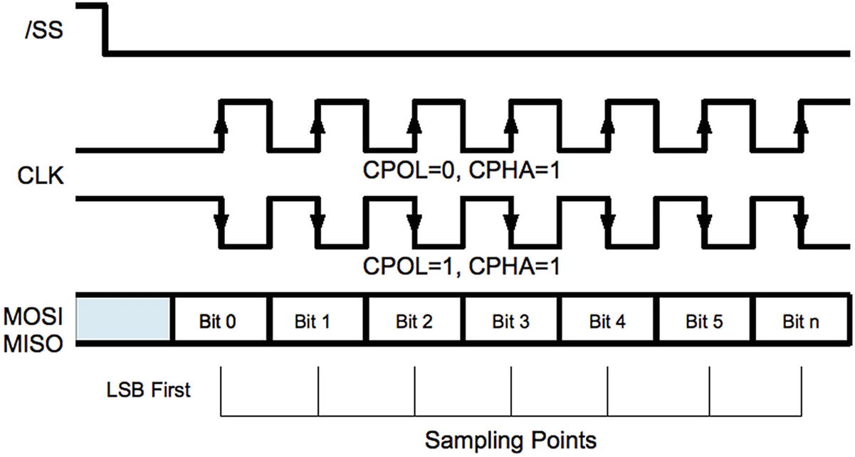
SPI signaling modes 1 and 3
While the four different modes can be confusing, it is important to realize that the data is sampled at the same times within the data bit cells. The data bit is always sampled at the midpoint of the data cell. When the clock phase is 0 (CPHA = 0), the data is sampled on the trailing edge of the clock, whether falling or rising according to CPOL. When the clock phase is 1 (CPHA = 1), the data is sampled on the leading edge of the clock, whether rising or falling according to CPOL.
Slave Selection
Raspberry Pi Built-in Chip Enable Pins
GPIO | Chip Enable | P1 |
|---|---|---|
8 |
| P1-24 |
7 |
| P1-26 |


The Raspbian Linux kernel driver supports the use of only these two chip enable lines. However, the driver is designed such that you don’t have to use them, or only these. It is possible, for example, to use a different GPIO pin as a select under user software control. The application simply takes responsibility for activating the slave select GPIO line prior to the data I/O and deactivates it after. When the driver is controlling the slave selects, this is done automatically.
Driver Support
SPI Device Nodes
Pathname | Bus | Device | GPIO |
|
|---|---|---|---|---|
/dev/spidev0.0 | 0 | 0 | 8 |
|
/dev/spidev0.1 | 0 | 1 | 7 |
|


If you open either of these device nodes with the C macro SPI_NO_CS, the node chosen makes no difference. Macro SPI_NO_CS indicates that slave select will be performed by the application instead of the driver, if any select is used at all. When only one slave device is attached, might it be possible to use a permanently hard-wired selected.
SPI API
Like I2C under Linux, the bare-metal API for SPI involves calls to ioctl(2) to configure the interface and for simultaneous read/write. The usual read(2) and write(2) system calls can be used for one-sided transfers.
Header Files
SPI Macro Definitions
Macro | Supported | Description |
|---|---|---|
SPI_CPOL | Yes | Clock polarity inverted (CPOL = 1) |
SPI_CPHA | Yes | Clock phase is 1 (CPHA = 1) |
SPI_MODE_0 | Yes | SPI Mode 0,0 (CPOL = 0, CPHA = 0) |
SPI_MODE_1 | Yes | SPI Mode 0,1 (CPOL = 0, CPHA = 1) |
SPI_MODE_2 | Yes | SPI Mode 1,0 (CPOL = 1, CPHA = 0) |
SPI_MODE_3 | Yes | SPI Mode 1,1 (CPOL = 1, CPHA = 1) |
SPI_CS_HIGH | Yes | Chip select is active high |
SPI_LSB_FIRST | No | LSB is transmitted first |
SPI_3WIRE | No | Use 3-Wire data I/O mode |
SPI_LOOP | No | Loop the MOSI/MISO data line |
SPI_NO_CS | Yes | Do not apply Chip Select |
SPI_READY | No | Enable extra Ready signal |
open(2): Opens the SPI device driver node
read(2): Reads but no transmission
write(2): Writes data while discarding received data
ioctl(2): For configuration and bidirectional I/O
close(2): Closes the SPI device driver node
In SPI communication, the use of read(2) and write(2) is generally unusual. Normally, ioctl(2) is used to facilitate simultaneous read/write transfers.
Open Device
The driver is normally opened for read and write (O_RDWR) because SPI usually involves reading and writing.
SPI Mode Macros
SPI Mode Macros
Macro | Effect | Comments |
|---|---|---|
SPI_CPOL | CPOL = 1 | Or use SPI_MODE_x |
SPI_CPHA | CPHA = 1 | Or use SPI_MODE_x |
SPI_CS_HIGH | SS is active high | Unusual |
SPI_NO_CS | Don’t assert select | Not used/application controlled |
The unsupported options are not shown, though one or more of these could be supported in the future.
Bits per Word
When the number of bits is not an even multiple of eight, the bits are assumed to be right-justified. For example, if the word length is set to 4 bits, the least significant 4 bits are transmitted. The higher-order bits are ignored.
Likewise, when receiving data, the least significant bits contain the data. All of this is academic on the Pi, however, since the driver supports only byte-wide transfers.
Clock Rate
Data I/O
SPI communication often involves transmitting data while simultaneously receiving data. For this reason, the read(2) and write(2) system calls cannot be used. The ioctl(2) call will, however, perform a simultaneous read and write.
On the Raspberry Pi, you will see example code that simply casts the pointers to unsigned long. The compiler automatically promotes these 32-bit values to a 64-bit value. This is safe on the Pi because the pointer value is 32 bits in size.
Note that to receive data, the master must always transmit data in order to shift data out of the slave peripheral. If any byte transmitted will do, you can omit the transmit buffer. Zero bytes will then be automatically transmitted by the driver to shift the slave data out.
The len structure member indicates the number of bytes for the I/O transfer. Receive and transmit buffers (when both used) are expected to transfer the same number of bytes.
The member speed_hz defines the clock rate that you wish to use for this I/O, in Hz. This overrides any value configured in the mode setup, for the duration of the I/O. The value will be automatically rounded down to a supported clock rate when necessary.
When the value speed_hz is 0, the previously configured clock rate is used (SPI_IOC_WR_MAX_SPEED_HZ).
When the delay_usecs member is non-zero, it specifies the number of microseconds to delay between transfers. It is applied at the end of a transfer, rather than at the start. When there are multiple I/O transfers in a single ioctl(2) request, this allows time in between so that the peripheral can process the data.
The bits_per_word member defines how many bits there are in a “word” unit. Often the unit is 1 byte (8 bits), but it need not be (but note that the Raspbian Linux driver supports only 8 bits or 9 in LoSSI mode).
When the bits_per_word value is 0, the previously configured value from SPI_IOC_WR_BITS_PER_WORD is used.
The cs_change member is treated as a Boolean value. When 0, no chip select is performed by the driver. The application is expected to do what is necessary to notify the peripheral that it is selected (usually a GPIO pin is brought low). Once the I/O has completed, the application then must then unselect the slave peripheral.
When cs_change is true, the driver asserts  for spidev0.0 and asserts
  for spidev0.1 prior to I/O and then deactivates the same upon completion. Of course, using these two nodes require two different open(2) calls.
The preceding example will perform three I/O transfers. Since the application never gets to perform any GPIO manipulation in between these I/Os, this applies to communicating with one particular slave device.
Here a single I/O transmission occurs, with data being sent from array tx and received into array rx. The return value from the ioctl(2) call returns the number of bytes transferred (32 in the example). Otherwise, -1 is returned to indicate that an error has occurred.
Close
Write
The write(2) system call can be used if the received data is unimportant. Note, however, that no delay is possible with this call.
Read
The read(2) system call is actually inappropriate for SPI since the master must transmit data on MOSI in order for the slave to send bits back on the MISO line. However, when read(2) is used, the driver will automatically send out zero bits as necessary to accomplish the read. (Be careful that your peripheral will accept zero bytes without unintended consequences.) Like the write(2) call, no delay is possible.
SPI Testing
When developing your SPI communication software, you can perform a simple loopback test to test your framework. Once the framework checks out, you can then turn your attention to communicating with the actual device.
While the SPI_LOOP mode bit is not supported by the Pi hardware, you can still physically loop your SPI bus by connecting a wire from the MOSI output back to the MISO input pin (connect GPIO 10 to GPIO 9).
A simple program, shown next, demonstrates this type of loopback test. It will write out 4 bytes (0x12, 0x23, 0x45, and 0x67) to the SPI driver. Because you have wired the MOSI pins to the MISO input, anything transmitted will also be received.
The spiloop.c SPI loopback program
Summary
The SPI bus and its operation were presented along with the C programming API. The chapter ended with a simple SPI loop test program. No extra hardware was required to run this.
That loop test provides a good coverage of the API being applied. The reader can take this one step further and access an actual slave device on the SPI bus. That last step adds the slave select to the overall picture and any command/response processing required of the device. You are now the SPI master!