Voiding in copper interconnects during electromigration
Abstract:
In this chapter, the void formation mechanism in copper interconnects is discussed. The void nucleation process is described, and the differences between aluminum and copper interconnects are highlighted. The void growth mechanism is presented, emphasizing the role that the copper/cap interface plays in electromigration. Immortality in copper interconnects is discussed in the context of no-void nucleation and void growth saturation.
5.1 Introduction
Electromigration has remained a reliability issue today even though the industry started to adopt copper as an interconnect material in early 2000. Although copper is expected to be much more electromigration resistant than aluminum owing to its smaller bulk diffusivity, the different metallization scheme between the two interconnect material leads to contrasting electromigration behavior. For copper interconnects with silicon dioxide as the inter-level and intra-level dielectric, void formation leading to opencircuit failure or unacceptable resistance increase is the main reliability concern, over the possibility of short-circuit failure owing to metallic extrusion. The presence of a weak Cu/dielectric cap interface leads to a low critical stress for void nucleation, as well as a fast diffusion path. This void nucleation mechanism is discussed in detail in 5.2. Owing to the ease of formation of voids in copper, the time-to-failure in copper interconnects depends mainly on the void growth time. In 5.3, the role played by the interfaces and grain boundaries during void migration and growth is discussed, as revealed through in situ scanning electron microscopy electromigration stressing. Although electromigration leads to void nucleation and growth, it does not necessarily lead to failure. Immortality in copper interconnects is discussed in 5.4 with regards to true immortality without void nucleation and probabilistic immortality with void growth saturation. Lastly, the impact of scaling and introduction of new materials into the copper interconnect scheme on electromigration is briefly discussed.
5.2 Void nucleation
5.2.1 Void nucleation theory
Void formation, which begins with void nucleation and subsequent void growth, is one of the failure modes induced by electromigration in interconnects. In order to nucleate a void in an interconnect, the void nucleation location must experience a divergence in vacancy flux resulting from electromigration, and the divergence in vacancy flux must give rise to a non-equilibrium high vacancy concentration (Lloyd, 1991). Although vacancy flux divergence can occur anywhere along the length of an interconnect, let us consider the cathode end of an interconnect where a diffusion barrier is present and assume the diffusion barrier to be a perfect blocking boundary for vacancy diffusion. Under this condition, the cathode end of the interconnect experiences an electromigration-induced vacancy flux divergence and also an increase in vacancy concentration during electromigration. As electromigration progresses and eventually generates a critically high concentration of vacancy at the cathode end of the interconnect, the excess vacancies coalesce to nucleate and form a stable void. The time to nucleate a void is inversely proportional to the square of the applied current density, as shown by a model that considers both the electromigration driving force and an opposing driving force that arises from the vacancy concentration gradient (Shatzkes and Lloyd, 1986).
It must be emphasized that in order to obtain a vacancy concentration that is higher than the equilibrium vacancy concentration, the cathode end of the interconnect in the above-mentioned scenario must not have a free surface. We can assume that free surface is absent in pre-stressed damascene Cu interconnect because the interconnect is usually surrounded by a Ta-based diffusion barrier at its base and side walls, and a dielectric capping layer on the top (Fig. 5.1). In the case of Al interconnect, free Al surfaces readily oxidise to form an adherent layer of Al oxide. The effect of a free surface is such that it will act as a sink for excess vacancies that are nearby, thereby resulting in a failure to build up a non-equilibrium high vacancy concentration. This occurs during void growth and is discussed in 5.3.
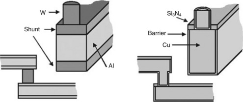
5.1 Schematics of Al and Cu interconnect architecture. Grain boundary is the dominant diffusion path in polygranular Al interconnect whereas Cu/dielectric cap interface is the dominant diffusion path in Cu interconnect.
If we consider that the vacancy concentration in the interconnect is in equilibrium with the hydrostatic stress acting on the interconnect (Blech and Herring, 1976), then the divergence in vacancy flux at the cathode end of the interconnect causes a tensile stress to evolve and, subsequently, nucleation of a stable void occurs when a critical tensile stress is attained. The relation between vacancy concentration and hydrostatic stress is given by (Korhonen et al., 1993):
where Cv is the vacancy concentration, Cvo is the equilibrium vacancy concentration in the absence of stress, Ω is the vacancy volume, σ is the hydrostatic stress, k is the Boltzmann constant and T is the temperature. It was reported that tensile stress and compressive stress arise at the cathode and anode ends of an interconnect, respectively, during electromigration testing and the interconnect returns to a state of uniform stress after the stress current is switched off (Blech and Herring, 1976). The stress evolution within an interconnect undergoing electromigration test can be described by the following one-dimensional model (Korhonen et al., 1993),
where t is the time, x is the direction along the length of the interconnect, Deff is the effective diffusivity of vacancy, B is the effective modulus of the metal–dielectric composite, Z* is the effective charge number, e is the fundamental charge and ρ is the resistivity of the conductor, and j is the applied current density.
5.2.2 Differences between aluminum and copper interconnects
Al and Cu interconnects follow different interconnect integration schemes, as shown in Fig. 5.1. Although bulk, grain boundary and interface diffusion paths are available in both Al and Cu interconnects, the dominant diffusion path in Al and Cu interconnects are grain boundary (Blech and Meieran, 1969; Rosenberg and Berenbaum, 1968) and Cu/dielectric cap interface (Hau-Riege and Thompson, 2001; Hu et al., 1999), respectively. Owing to the different dominant diffusion paths, several different electromigration behaviours are observed in Al and Cu interconnects. Al interconnects have longer electromigration lifetimes when they have a bamboo-like microstructure compared with a polygranular microstructure (Cho and Thompson, 1989; Vaidya et al., 1980), but the lifetimes of Cu interconnects are independent of the type of microstructure (Hau-Riege and Thompson, 2001). Longer electromigration lifetimes are observed in Al interconnects with bamboo-like microstructure because a continuous grain boundary path for diffusion along the electromigration direction is absent, and this slows down the rate of mass transport. A bamboo-like microstructure does not improve the lifetime of Cu interconnect because its dominant diffusion path is not along the grain boundary. The electromigration lifetime of Cu interconnects is found to be independent of width scaling since mass diffusion takes place along the Cu/dielectric cap interface (Hu et al., 1999; Usui et al., 2005).
Besides being the dominant diffusion path in Cu interconnect, the Cu/ dielectric cap interface was also reported to be the preferred void nucleation site (Meier et al., 1999; Hau-Riege, 2002). This resulted in Cu interconnects exhibiting longer electromigration lifetimes in via-below interconnect configuration, than in via-above interconnect configuration (Gan et al., 2001; 2005), as shown in Fig. 5.2. The observation of lifetime dependence on structural configuration can be explained by the void size required to induce an electromigration failure (Fig. 5.3). For the case where the via is located below the interconnect, a void that nucleates at the Cu/dielectric cap interface is required to grow and span the entire thickness of the interconnect before the flow of electric current is obstructed. For the other case where the via is located above the interconnect, a void that nucleates at the Cu/dielectric cap interface can easily obstruct the flow of electric current even when it partially spans the thickness of the interconnect.
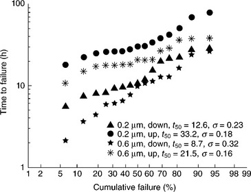
5.2 Times-to-failure for 0.2 μm-wide and 0.6 μm-wide SiN-capped Cu interconnects in both the upstream (via-below) and downstream (via-above) test configurations. The test condition is T = 370 °C and j = 2.0 MA cm−2 (Gan et al., 2005).
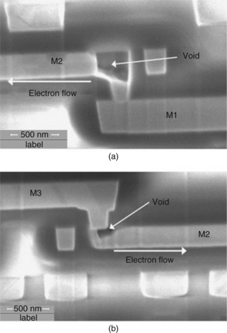
5.3 SEM cross-section images of failed 0.2 μm-wide SiN-capped Cu interconnects in (a) downstream (via-above) and (b) upstream (via-below) configurations. A partially-spanned void is only needed in (a) to cause failure whereas a fully-spanned void is required in (b). (Gan et al., 2005).
The critical stress for void nucleation was reported to be between 350 and 600 MPa in Al interconnects (Hau-Riege and Thompson, 2000; 2001) and ranges from less than 41 to 246 MPa (Choi et al., 2009; Hau-Riege, 2002; Hau-Riege et al., 2004) in Cu interconnects. It can be seen that a relatively low tensile stress is needed to nucleate a void in Cu interconnects. The relative ease of nucleating a void in Cu interconnects can also be inferred from the current density exponent of 1 that is observed experimentally (Filippi et al., 2006; Hu and Rosenberg, 1999). On the other hand, the current density exponent of Al interconnects is reported to be 2. Current density exponent is a parameter in Black’s model (Black, 1967):
where t50 is the median time to failure, A is a constant, j is the current density, n is the current density exponent and Ea is the activation energy for diffusion. An electromigration failure process gives rise to a current density exponent of 1 if void growth is the failure rate determining step (Lloyd, 1991), whereas a current density exponent of 2 is observed if void nucleation is the failure rate determining step (Shatzkes and Lloyd, 1986). Thus, a current density exponent of 1 for Cu interconnects implies that void nucleation time is short compared with void growth time, owing to the low critical stress for void nucleation.
5.3 Void growth
5.3.1 Theory of void growth
Electromigration induces a void growth process when there is a depletion of Cu atoms at locations where there is an existing void. This requires electromigration to induce a vacancy flux divergence at the location of the void. The excess of vacancies that arises from the electromigration-induced vacancy flux divergence is driven to the void, by a hydrostatic stress gradient, such that the vacancy concentration in the vicinity of the void remains close to the equilibrium vacancy concentration level. The void acts as a vacancy sink because an excess of vacancies gives rise to tensile stress, as seen from equation [5.1], while the surface of a void is stress free because the void surface is not constrained. The differences in the hydrostatic stresses therefore give rise to a driving force for the excess of vacancies in the vicinity of the void to diffuse to the void surface. The void grows larger as vacancies are added to it. The volume of the void increases with time as given by (Tu, 2003):
where V is the void volume, Ω is the vacancy volume, JEM is the vacancy flux that arises from electromigration, A is the cross-sectional area of vacancy flux and t is the time.
5.3.2 Void growth mechanisms
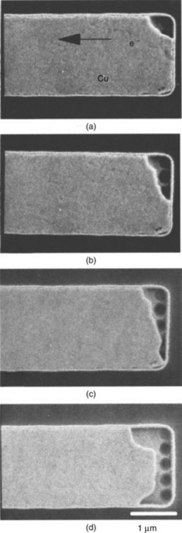
In situ electromigration experiments have been carried out to observe the developments in a void growth process (Meier et al., 1999; Liniger et al., 2002; Vairagar et al., 2004b; Choi et al., 2008). In unpassivated Cu interconnects, Cu grains are noticed to thin down from the top free surface to the bottom Ta-based diffusion barrier as the void grows in size (Liniger et al., 2002). Grain thinning is observed to occur at the cathode end of the Cu interconnect where the presence of Ta-based diffusion barrier gives rise to flux divergence (Fig. 5.4). The occurrence of surface grain thinning is evidence that surface diffusion is the dominant diffusion path in unpassivated Cu interconnects. The same study also reported the occurrence of an edge displacement type of void growth where surface grain thinning is absent. In the edge displacement type void growth mechanism, the void is observed to start growing from the cathode end of the interconnect. A vertical interface is maintained between the void and Cu grains as the void grows, as shown in Fig. 5.5. Void growth by either surface grain thinning or edge displacement is believed to have a dependence on the local microstructure of the Cu interconnects. Grain orientation, which affects the surface energy of the void front, grain boundary orientation angle and coherency of the Cu/Ta interface, is believed to influence the void growth mechanism and void shape. This is supported by the observation of an irregular void front as shown in Fig. 5.5 after 12 h of electromigration stressing.
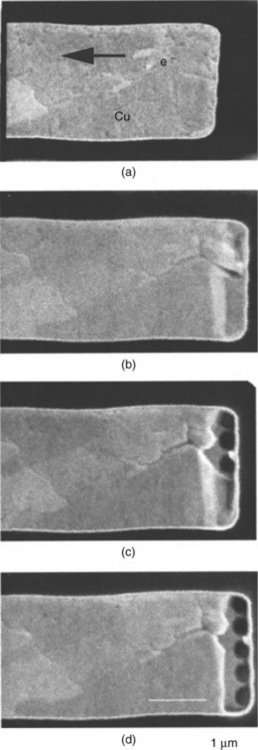
5.4 Top view SEM images of unpassivated Cu interconnects showing surface grain thinning during void growth: (a) the beginning of the electromigration test; (b) after 2.7 h of stressing, grain thinning is visible at the cathode end of the Cu interconnect; (c) after 5.9 h of stressing, vias located at the bottom of the Cu interconnects are visible; (d) after 8.8 h of testing, all vias can be seen (Liniger et al., 2002).
5.5 Top view SEM images of unpassivated Cu interconnects showing edge displacement type of void growth: (a) a void formed at the corner of the Cu interconnect after 5 h of stressing; (b) a larger void is observed after 8 h and (c) after 10 h of stressing; (d) a void with irregular void front can be seen after 12 h of electromigration stress (Liniger et al., 2002).
In addition to surface grain thinning and edge displacement void growth, voids are observed to form at a distance away from the cathode end of the Cu interconnects and subsequently drift towards the cathode in passivated Cu interconnects (Vairagar et al., 2004b). Voids are seen to drift in passivated Cu interconnects because Cu surface self-diffusion has an activation energy of 0.5 eV (Hu et al., 1999) which is lower than that of 0.9 eV for diffusion at the Cu/dielectric cap interface (Choi et al., 2007; Usui et al., 2005). It was further reported that voids are observed to grow as they drift along the Cu interconnects (Choi et al., 2008). Failure occurs when the void spans the entire width and thickness of the Cu interconnects, and this may even occur before the void reaches the cathode end (Choi et al., 2008).
In situ experiments on passivated interconnects observed that drifting voids can be pinned at grain boundaries, and may subsequently be de-pinned such that the voids continue to drift towards the cathode (Choi et al., 2008; Vairagar et al., 2004b). Energy is needed to de-pin voids that are trapped at grain boundaries, and the required magnitude of energy increases with increasing void size. It is therefore observed that large voids are unable to de-pin themselves from grain boundaries and these voids subsequently grow larger in place and give rise to failure (Choi et al., 2008). On the other hand, a void continues to drift towards the cathode end of the Cu interconnect if it manages to de-pin itself from the grain boundary. The drift velocity is dependent on the applied current density and the surface diffusivity, where the surface diffusivity has been reported to vary with grain orientation (Choi et al., 2007).
5.3.3 Effect of metal capping layer
The rate of void growth in Cu interconnects is largely determined by the mass transport at the Cu/dielectric cap interface since that is the dominant diffusion path in Cu interconnects (Hau-Riege and Thompson, 2001; Hu et al., 1999). The drift velocity of Cu atoms or void front can be expressed by:
As Cu interconnects are surrounded by Ta-based diffusion barrier at the base and side walls, and a dielectric capping layer is deposited on the top, the effective diffusivity in the Cu interconnects is given by:
where the subscripts B, GB, I and S refer to bulk (lattice), grain boundary, interface (i.e. Cu/Ta interface) and surface (i.e. Cu/SiNx interface) respectively; δGB, δI and δS refer to the widths of grain boundary, interface and surface, respectively; d is the grain size, h is the line thickness, w is the line width, and nB, (δGB/d), δI(1/h + 2/w) and δS(1/h) are the fractions of atoms diffusing through the bulk, grain boundary, interface and surface of the Cu interconnect, respectively.
Various reports have shown that longer Cu electromigration lifetime is observed when the Cu/dielectric cap interface is replaced with a Cu/metal cap interface (Gambino, 2010; Hu et al., 2002). It was reported that a longer electromigration lifetime is attributed to the higher bond strength Cu/metal cap interface, which causes a reduction in the void growth rate in Cu interconnects with Cu/metal cap interface as compared to those with Cu/dielectric cap interface (Lloyd et al., 2002). Higher adhesion energy between Cu and capping layer is shown to increase the activation energy for electromigration and, hence, reduce the rate of void growth which in turn enhances the electromigration lifetime (Lloyd et al., 2002; Lane et al., 2003). Hu et al. (2003) reported a change in the dominant diffusion path from Cu/ capping layer interface to grain boundary when the top surface of Cu is coated with CoWP as shown in Fig. 5.6. When a CoWP cap is employed as the capping layer, it was further observed that Cu interconnects having bamboo-like microstructure give rise to higher electromigration lifetime than Cu interconnects with polygranular microstructure (Hu et al., 2003). Activation energies of 1.0 and 1.9 eV are reported for CoWP-capped Cu interconnects with polygranular and bamboo-like microstructure, respectively (Hu et al., 2003). An activation energy of 1.0 eV is similar to that of Cu grain boundary diffusion (Mishra et al., 1988), whereas an activation energy of 1.9 eV is close to the reported value of 2.07 eV for Cu bulk diffusion (Peterson, 1978).
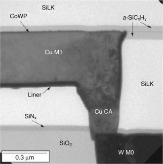
5.6 TEM cross-section image of Cu interconnect coated with a CoWP capping layer (Hu et al., 2003).
5.3.4 Effects of pre-existing voids in copper interconnects
Voids may exist in as-fabricated Cu interconnects (Fig. 5.7) when thermal mismatch between Cu and the surrounding dielectric materials give rise to stress-induced voiding during wafer fabrication. Pre-existing voids can significantly affect the electromigration lifetime because these voids can shorten the time to achieve a fatal void size. The size and number of preexisting voids per unit surface area was reported to increase with increasing interconnect width, hence resulting in an electromigration lifetime that deteriorates with increasing interconnect width (Chang et al., 2007).
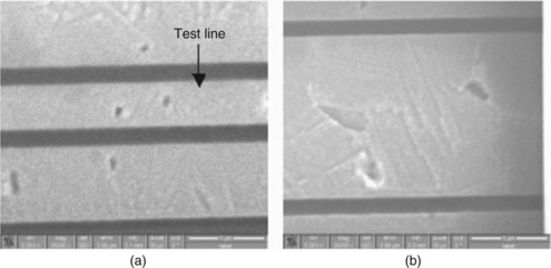
5.7 Top view SEM images of (a) 0.61 μm and (b) 2.25 μm wide as-fabricated Cu interconnects. Microvoids can be seen at the top surface of Cu interconnects, which is at the Cu/dielectric cap interface. (Chang et al., 2007).
Although electromigration physics and experiments have shown that the lifetimes of Cu interconnects without pre-existing voids are independent of the interconnect width (Hu et al., 1999; Usui et al., 2005), the existence of these voids can lead to an erroneous lifetime prediction when the interconnect width is scaled. In addition, voids can drift towards the cathode, grow larger in size when drifting or when pinned at grain boundary, and coalesce with other voids (Choi et al., 2008; Meier et al., 1999; Meyer et al., 2002; Vairagar et al., 2004a). Therefore, the size and initial location of pre-existing voids and their subsequent motion increases the uncertainty of reliability prediction.
It was further suggested that voids located at a distance away from the cathode end of Cu interconnects, as observed in post-electromigration failure analysis, evolved from pre-existing voids (Choi et al., 2011). Simulation results showed that a pre-existing void will grow if it is within a critical distance from the cathode end of the Cu interconnect. This critical distance is inversely related to the magnitude of current density carried by the interconnect, and this inverse relation is governed by the Blech Effect (Blech, 1976) which will be discussed in detail in Section 5.4. When the preexisting void is within a critical distance from the cathode end of the Cu interconnect, the Blech Effect prevents atomic flux from entering the preexisting void from the cathode-side void front, while a continuous stream of atomic flux leaves from the anode-side void front, thereby causing the pre-existing void to grow. In the case where the pre-existing void is located along the middle of the Cu interconnect, where the Blech Effect is absent, the pre-existing void will grow if the Cu grain adjacent to the anode-side void front has higher diffusivity than the Cu grain adjacent to the cathode-side void front. These simulation results suggest that the electromigration lifetime of Cu interconnect has a stronger dependence on the applied current density and the grain diffusivity when pre-existing voids are present, and the reliability prediction of Cu interconnects is complicated by the location and size of pre-existing voids.
5.4 Immortality
5.4.1 Criteria for immortality
During electromigration, a stress gradient-induced back-stress force is induced such that the net atomic flux is given by:
where Ca is the atomic concentration, and the rest of the terms are as previously defined. A steady-state condition can occur in which the stress gradient induced back-stress force balances the electron wind force, such that the hydrostatic stress is time-invariant and linear along the line length (Blech, 1976) as illustrated in Fig. 5.8. Under this condition, the net atomic flux along the line is zero. From equation [5.7],
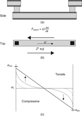
5.8 Schematics illustrating the conditions for immortality in a straight via-to-via line without void nucleation: (a) side view and (b) top view of an interconnect with the arrows showing the direction of electron flow, electron wind force and back-stress; (c) stress as a function of location along the interconnect at different times. The line will be immortal if the maximum steady-state stresses are less than σnuc and σext.
where L is the length of the line and Δσmax is the stress difference between the anode and the cathode.
If the critical tensile stress for void nucleation σnuc is greater than the maximum steady-state tensile stress developed in the line, no void forms and the line does not fail, i.e. it is immortal. For the tensile stress at the cathode to be equivalent to σnuc, Δσmax can be expressed as:
where σ0 is the initial stress in the metal line owing to the thermal mismatch with the dielectric system.
Through the rearrangement of equation [5.8], we can derive a critical current-density line-length product (jL)crit that defines this condition for immortality or commonly known as the ‘Blech Effect’, whereby no void nucleation occurs as:
This means that short lines and/or lines stressed at low current densities are more likely to be immortal.
On the other hand, if (jL) exceeds (jL)crit,nuc, void nucleation occurs. However, if the void that forms in the metal line does not completely block off the current flow, it is not fatal. In Al technology, Ti-based overlayers and underlayers offer alternative paths for the current flow. Thus, a void can continue to grow as the current is shunted around it through the refractory metal layers, until the electron wind force and the back-stress force balance again. In this case, the line is immortal if the resistance increase associated with the void volume is lower than the maximum acceptable resistance increase ΔRmax and the maximum compressive stress in the line does not cause yielding or fracture of the surrounding dielectric as illustrated in Fig. 5.9. In this case, the immortality condition owing to resistance saturation is given by (Filippi et al., 1995)
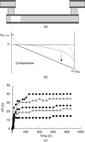
5.9 Schematics illustrating the conditions for immortality in straight via-to-via lines with void nucleation: (a) side view of an interconnect; (b) Stress as a function of location along the interconnect at different times. (c) Experimentally reported observations of resistance saturation in Al interconnects, reproduced from (Filippi et al., 1995). The line will be immortal if the maximum resistance increase is less than the specified failure criterion.
where ρ and A are the resistivity and cross-sectional area of the high-conductivity metal, respectively, ρ1 and A1 are the resistivity and cross-sectional area of the shunt layer, respectively, and R is the initial resistance of the line. For copper interconnects, immortality owing to resistance saturation is possible if the Ta-based liner is reliable enough to shunt the current when a void spans the whole cross-sectional area of the interconnect.
5.4.2 Short length effect in copper interconnects
Short length effect or immortality is only possible if the interconnect is constrained such that a back-stress force can develop to balance the electron wind force. In aluminum interconnects, immortality can be observed for a drift-type or ‘Blech-type’ structure, which is an unpassivated aluminum line with a more electromigration-resistant metal underlayer, owing to the formation of a self-passivating aluminum oxide. Early work on Cu drift-type structures reported a (jL)crit of 900–1600 A cm−1 for a temperature range of 175–225 °C, with a transition to 225–900 A cm−1 for an increased temperature of 250–275 °C (Frankovic and Bernstein, 1996). The decrease in (jL)crit at higher temperature is believed to result from a change in the yield stress of copper as (jL)crit is theoretically temperature independent. For Cu damascene structures, different (jL)crit values have been reported, depending whether it is single or dual damascene. A single damascene structure is constrained by its surrounding liner and dielectric, whereas a dual damascene structure has vias connected at the ends. Study of short length effects using dual damascene Cu structures complicates the analysis because of the possibility of voids forming in the vias, leading to early failures (Ogawa et al., 2001). However, these early failures are more probably caused by processing issues, such as the weakness of the Ta liner, that lead to a reduced back-stress effect.
In mature interconnect technology, (jL)crit depends not on whether it is a single damascene or dual damascene structure, but on the location of the via at the cathode end of the test line. For a via-above (at the cathode side of the test line) structure, true immortality requires that the condition for void nucleation is not reached, as a small void that forms directly below the via can completely block electron current flow because the dielectric cap does not shunt current. On the other hand, in a via-below structure, true immortality only requires that the void at the Cu/dielectric cap interface does not grow to become full spanning across the width and height of the interconnect. Thus, the reported lower (jL)crit value of 1500 A cm−1 by Hau-Riege et al. (2004) corresponds to the equivalent (jL)crit,nuc in Cu lines, as expressed in equation [5.10], because a via-above structure was used in their experiments. On the other hand, Lee et al. (2001) used a via-above structure and obtained a larger value of 3700 A cm−1, corresponding to the equivalent (jL)crit,sat in Cu lines as expressed in equation [5.11].
Another short length study on Cu interconnect with SiO2 intra-level dielectric had reported a (jL)crit,nuc < 2100 A cm−1 (Hau-Riege, 2002), with a probabilistic characteristic of immortality. This means that at a (jL) of 2100 A cm−1, 100% immortality was not observed in the via-above structure. Failure analysis revealed the presence of voids in all stressed samples, but the location varied (Fig. 5.10). If the void was directly below the via, an open-circuit failure was observed. However, if the void was a distance away from the via, no resistance change was detected. This observation can be explained by noting that a (jL) of 2100 A cm−1 is between (jL)crit,nuc and (jL)crit,sat. Thus, a void always forms but saturates, under this stress condition. Depending on its location, this partial spanning void only causes an opencircuit failure if it is located directly below the via that cuts off the current flow.
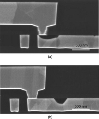
5.10 SEM cross-section image of a void formed (a) directly below a via that caused an open-circuit failure and (b) at a distance away from the cathode end of a Cu interconnect which remains immortal. (Hau-Riege, 2002).
5.5 Future trends
5.5.1 Shrinkage in interconnect dimension
As interconnect dimensions continue to shrink in accordance with Moore’s law, electromigration failures owing to voiding are exacerbated. This is because the critical void volume to cause an open-circuit failure or significant increase in resistance decreases with the cross-sectional area of the interconnect. As a result, a lower amount of mass transport of Cu atoms is needed to cause a failure, thus shortening the electromigration lifetime. To mitigate this problem, a different metallic cap material such as CoWP may be required (Gambino et al., 2006), that not only reduces the drift velocity along the Cu/cap interface, but also provides a current shunt for via-above structures.
Improvements in interconnect layout and design may also delay the onset of electromigration failure. Having a line extension beyond the via at the cathode end of the interconnect creates an extra volume of copper to be depleted without impacting on the resistance of the line as shown schematically in Fig. 5.11 (Shao et al., 2004). This line extension, commonly known as the reservoir, delays the onset of failure. On the other hand, extra vias can be designed at the cathode as well (Girault et al., 2008). The effect is similar to having a reservoir that stretches from the end of the line to the first via, as it increases the void volume required to disconnect the current path from the vias to the line.
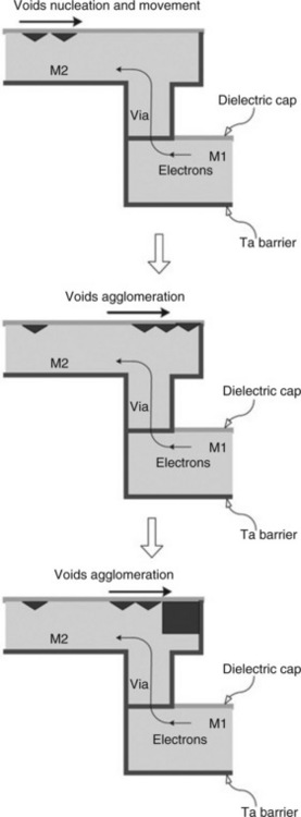
5.11 Schematic showing the effects of having a reservoir at the cathode end, whereby voids can accumulate without impacting the line resistance. (Shao et al., 2004).
5.5.2 Low-k dielectrics
The void formation mechanism in copper interconnects is the main reliability concern with silicon dioxide as the inter-level and intra-level dielectric. As new dielectric materials with lower dielectric constant (low-k) are introduced to improve the interconnect delay performance, the void nucleation and growth processes will change (Hau-Riege, 2004). New processes for the low-k dielectric and new dielectric cap material will lead to a decrease in the critical stress for void nucleation, which is known to be very sensitive to process variation. The weakening of the Cu/dielectric cap interface will also increase the mass transport rate, thus shortening electromigration lifetime. Moreover, low-k materials have low bulk modulus, which delays the build-up of back-stress and thus decreases the possibility of immortality. This lower bulk modulus also increases the likelihood of extrusion failures.
5.6 Acknowledgements
The authors would like to acknowledge the insightful discussions he had with Professor Carl V. Thompson (Massachusetts Institute of Technology).
5.7 References
Black, J.R. Electromigration failure modes in aluminium metallization for semiconductor devices. Proceedings of the IEEE 6th annual reliability physics symposium. 1967:1587–1594.
Blech, I.A. Electromigration in thin aluminum films on titanium nitride. J Appl Phys. 1976; 47:1203–1208.
Blech, I.A., Herring, C. Stress generation by electromigration. Appl Phys Lett. 1976; 29:131–133.
Blech, I.A., Meieran, E.S. Electromigration in thin Al films. J Appl Phys. 1969; 40:485–491.
Chang, C.W., Thompson, C.V., Gan, C.L., Pey, K.L., Choi, W.K., Lim, Y.K. Effects of microvoids on the linewidth dependence of electromigration failure of dual-damascene copper interconnects. Appl Phys Lett. 2007; 90:193505.
Cho, J., Thompson, C.V. Grain size dependence of electromigration-induced failures in narrow interconnects. Appl Phys Lett. 1989; 54:2577–2579.
Choi, Z.-S., Lee, J.H., Lim, M.K., Gan, C.L., Thompson, C.V. Void dynamics in copper-based interconnects. J Appl Phys. 2011.
Choi, Z.-S., Mönig, R., Thompson, C.V. Dependence of the electromigration flux on the crystallographic orientations of different grains in polycrystalline copper interconnects. Appl Phys Lett. 2007; 90:241913.
Choi, Z.-S., Mönig, R., Thompson, C.V. Effects of microstructure on the formation, shape, and motion of voids during electromigration in passivated copper interconnects. J Mater Res. 2008; 23:383–391.
Choi, Z.-S., Park, B.-L., Lee, J.M., Choi, G.-H., Lee, H.-D., Moon, J.-T. Electromigration tests for critical stress and failure mechanism evaluation in Cu/W via/Al hybrid interconnect. Proceedings of the IEEE international reliability physics symposium. 2009; 828–831.
Filippi, R.G., Biery, G.A., Wachnik, R.A. The electromigration short-length effect in Ti-AlCu-Ti metallization with W studs. J Appl Phys. 1995; 78:3756–3768.
Filippi, R.G., Christiansen, C., Li, B., Gill, J., McLaughlin, P.S., Demarest, J.J., Wang, P.-C. Electromigration results with large sample size for dual damascene structures in a copper/CVD low-k dielectric technology. Proceedings of the IEEE international interconnect technology conference. 2006; 98–100.
Frankovic, R., Bernstein, G.H. Electromigration drift and threshold in Cu thin-film interconnects. IEEE Trans Electron Devices. 1996; 46:2233–2239.
Gambino, J.P. Improved reliability of copper interconnects using alloying. Proceedings of the IEEE 17th international symposium on the physical and failure analysis of integrated circuits. 2010; 1–7.
Gambino, J., Wynne, J., Gill, J., Mongeon, S., Meatyard, D., Lee, B., Bamnolker, H., Hall, L., Li, N., Hernandez, M., Little, P., Hamed, M., Ivanov, I., Gan, C.L. Self-aligned metal capping layers for copper interconnects using electroless plating. Microelectronic Engineering. 2006; 83:2059–2067.
Gan, C.L., Thompson, C.V., Pey, K.L., Choi, W.K., Tay, H.L., Yu, B., Radhakrishnan, M.K. Effect of current direction on the lifetime of different levels of copper dual-damascene metallization. Appl Phys Lett. 2001; 79:4592–4594.
Gan, C.L., Lee, C.Y., Cheng, C.K., Gambino, J. Materials, technology and reliability of advanced interconnects-2005. In: Besser P.R., McKerrow A.J., Iacopi F., Wong C.P., Vlassak J., eds. Effect of current direction on the reliability of different capped Cu interconnects. Warrendale: MRS; 2005:289–294.
Girault, V., Terrier, F., Ney, D. Reservoir effect in SiCN capped copper/SiO2 interconnects. Microelectron Reliab. 2008; 48:219–224.
Hau-Riege, C.S. An introduction to Cu electromigration. Microelectron Reliab. 2004; 44:195–205.
Hau-Riege, C.S., Thompson, C.V. The effects of microstructural transitions at width transitions on interconnect reliability. J Appl Phys. 2000; 87:8467–8472.
Hau-Riege, C.S., Thompson, C.V. Electromigration in Cu interconnects with very different grain structures. Appl Phys Lett. 2001; 78:3451–3453.
Hau-Riege, C.S., Hau-Riege, S.P., Marathe, A.P. The effect of interlevel dielectric on the critical tensile stress to void nucleation for the reliability of Cu interconnects. J Appl Phys. 2004; 96:5792–5796.
Hau-Riege, S.P. Probabilistic immortality of Cu damascene interconnects. J Appl Phys. 2002; 91:2014–2022.
Hau-Riege, S.P., Thompson, C.V. Experimental characterization and modelling of the reliability of interconnect trees. J Appl Phys. 2001; 89:601–609.
Hu, C.-K., Rosenberg, R. Scaling effect on electromigration in on-chip Cu wiring. Proceedings of the IEEE international interconnect technology conference. 1999; 267–269.
Hu, C.-K., Gignac, L., Rosenberg, R., Liniger, E., Rubino, J., Sambucetti, C., Domenicucci, A., Chen, X., Stamper, A.K. Reduced electromigration of Cu wires by surface coating. Appl Phys Lett. 2002; 81:1782–1784.
Hu, C.-K., Gignac, L., Rosenberg, R., Liniger, E., Rubino, J., Sambucetti, C., Stamper, A., Domenicucci, A., Chen, X. Reduced Cu interface diffusion by CoWP surface coating. Microelectronics Engineering. 2003; 70:406.
Hu, C.-K., Rosenberg, R., Lee, K.Y. Electromigration path in copper thin-film lines. Appl Phys Lett. 1999; 74:2945–2947.
Korhonen, M.A., Børgesen, P., Tu, K.N., Li, C.-Y. Stress evolution due to electromigration in confined metal lines. J Appl Phys. 1993; 73:3790–3799.
Lane, M.W., Liniger, E.G., Lloyd, J.R. Relationship between interfacial adhesion and electromigration in Cu metallization. J Appl Phys. 2003; 93:1417–1421.
Lee, K.-D., Ogawa, E.T., Matsuhashi, H., Justison, P.R., Ko, K.S., Ho, P.S. Electromigration critical length effect in Cu/oxide dual-damascene interconnects. Appl Phys Lett. 2001; 79:3236–3238.
Liniger, E., Gignac, L., Hu, C.-K., Kaldor, S. In situ study of void growth kinetics in electroplated Cu lines. J Appl Phys. 2002; 92:1803–1810.
Lloyd, J.R. Electromigration failure. J Appl Phys. 1991; 69:7601–7604.
Lloyd, J.R., Lane, M.W., Liniger, E.G. Relationship between interfacial adhesion and electromigration in Cu metallization. IEEE international integrated reliability workshop. 2002; 32–35.
Meier, N.E., Marieb, T.N., Flinn, P.A., Gleixner, R.J., Bravman, J.C. In-situ studies of electromigration voiding in passivated copper interconnects. AIP Conf Proc. 1999; 491:180–185.
Meyer, M.A., Herrmann, M., Langer, E., Zschech, E. In situ SEM observation of electromigration phenomena in fully embedded copper interconnect structures. Microelectron Eng. 2002; 64:375–382.
Mishra, R.S., Jones, H., Greenwood, G.W. An empirical correlation for the grain-boundary diffusion of impurities in copper. J Mater Sci Lett. 1988; 7:728–730.
Ogawa, E.T., Bierwag, A.J., Lee, K.D., Matsuhashi, H., Justison, P.R., Ramamurthi, A.N., Ho, P.S., Blaschke, V.A., Griffiths, D., Nelsen, A., Breen, M., Havemann, R.H. Direct observation of a critical length effect in dual-damascene Cu/oxide interconnects. Appl Phys Lett. 2001; 78:2652–2654.
Peterson, L. Self-diffusion in pure metals. J Nucl Mater. 1978; 69–70:3–37.
Rosenberg, R., Berenbaum, L. Resistance monitoring and effects of nonadhesion during electromigration in aluminum films. Appl Phys Lett. 1968; 12:201–204.
Shao, W., Vairagar, A.V., Tung, C.-H., Xie, Z.-L., Krishnamoorthy, A., Mhaisalkar, S.G. Electromigration in copper damascene interconnects: reservoir effects and failure analysis. Surface Coatings Technol. 2004; 198:257–261.
Shatzkes, M., Lloyd, J.R. A model for conductor failure considering diffusion concurrently with electromigration resulting in a current exponent of 2. J Appl Phys. 1986; 59:3890–3893.
Tu, K.N. Recent advances on electromigration in very-large-scale-integration of interconnects. J Appl Phys. 2003; 94:5451–5473.
Usui, T., Nasu, H., Watanabe, T., Shibata, H., Oki, T., Hatano, M. Electromigration diffusion mechanism of electroplated copper and cold/hot two-step sputter-deposited aluminum–0.5-wt% copper damascene interconnects. J Appl Phys. 2005; 98:063509.
Vaidya, S., Fraser, D.B., Lindenberger, W.S. Electromigration in fine-line sputter-gun Al. J Appl Phys. 1980; 51:4475–4482.
Vairagar, A.V., Mhaisalkar, S.G., Krishnamoorthy, A., Tu, K.N., Gusak, A.M., Meyer, M.A., Zschech, E. In situ observation of electromigration-induced void migration in dual-damascene Cu interconnect structures. Appl Phys Lett. 2004; 85:2502–2504.
Vairagar, A.V., Mhaisalkar, S.G., Krishnamoorthy, A., Tu, K.N., Gusak, A.M., Zaporozhets, T., Meyer, M.A., Zschech, E. Study of electromigration induced void nucleation, growth, and movement in Cu interconnects. AIP Conf Proc. 2004; 741:135–147.


