Modeling, simulation, and X-ray microbeam studies of electromigration
Abstract:
Modeling and simulation coupled with X-ray microbeam studies, where local elastic strains are measured, can be used to resolve some of the challenging questions regarding the physics of electromigration. This chapter provides an introduction to the prevalent modeling methodology and three key issues that are currently unresolved: (i) how does the diffusing mass arrange itself and the effect of diffusion path, (ii) what is the appropriate driving stress, and (iii) determination of effective charge number Z*. Analytic and finite element modeling formulations are presented and used with two X-ray microbeam data sets, exhibiting opposing trends, to demonstrate how these questions may be answered.
3.1 Introduction
Models for predicting stress evolution during electromigration in metallic interconnect lines start with an equation for the atomic or vacancy flux, which, for the case of the atomic flux vector J, typically has a form like (Korhonen et al. 1993):
where D is an average mass transport diffusion coefficient, k is the Boltzmann constant, T is the absolute temperature, ρ is the electrical resistivity, e is the elementary charge, Z* is the effective charge number, j is the current density, Ω is the atomic volume, and ![]() is a stress (tensile taken as positive here). The stress in Eqn. [3.1] is taken as either the normal stress on a grain boundary (Blech and Herring 1976, Gleixner and Nix 1999, Korhonen et al. 1993, Povirk 1997) or the hydrostatic stress (Hau-Riege and Thompson 2000, Sarychev et al. 2000, Wang et al. 1998). The first term on the right hand side in the parentheses represents the atomic driving force associated with the electric current (the electromigration driving force), and the second term represents the mechanical driving force. A similar equation results when vacancy fluxes are considered, but in the opposing direction since the mass diffusion process is associated with the exchange of atoms and vacancies. The divergence of the atomic flux vector J is associated with the depletion (when the divergence is positive) or the accumulation (when the divergence is negative) of material at a point in the interconnect line. If the interconnect line is confined, the depletion or accumulation of material at any given location leads to a change in the stress state, which causes an increase in the mechanical driving force in equation [3.1] acting to oppose the electromigration induced mass flux. If the conductor line has flux blocking boundaries at each end and is embedded in a confining dielectric material, and if the line and confining material do not fail (i.e. the current density j is below some critical value), an equilibrium state of zero atomic flux (J = 0) results along the line after sufficient time for the electromigration and stress driven diffusion terms to balance. Some studies proposed extensions to equation [3.1] including Park et al. (1999) who add the effect of alloying elements on the chemical potential driving force and Sarychev et al. (2000) who consider the effect of a non-equilibrium vacancy concentration field. In this chapter, we ignore these effects, which are typically second order, and only consider the basic equation [3.1].
is a stress (tensile taken as positive here). The stress in Eqn. [3.1] is taken as either the normal stress on a grain boundary (Blech and Herring 1976, Gleixner and Nix 1999, Korhonen et al. 1993, Povirk 1997) or the hydrostatic stress (Hau-Riege and Thompson 2000, Sarychev et al. 2000, Wang et al. 1998). The first term on the right hand side in the parentheses represents the atomic driving force associated with the electric current (the electromigration driving force), and the second term represents the mechanical driving force. A similar equation results when vacancy fluxes are considered, but in the opposing direction since the mass diffusion process is associated with the exchange of atoms and vacancies. The divergence of the atomic flux vector J is associated with the depletion (when the divergence is positive) or the accumulation (when the divergence is negative) of material at a point in the interconnect line. If the interconnect line is confined, the depletion or accumulation of material at any given location leads to a change in the stress state, which causes an increase in the mechanical driving force in equation [3.1] acting to oppose the electromigration induced mass flux. If the conductor line has flux blocking boundaries at each end and is embedded in a confining dielectric material, and if the line and confining material do not fail (i.e. the current density j is below some critical value), an equilibrium state of zero atomic flux (J = 0) results along the line after sufficient time for the electromigration and stress driven diffusion terms to balance. Some studies proposed extensions to equation [3.1] including Park et al. (1999) who add the effect of alloying elements on the chemical potential driving force and Sarychev et al. (2000) who consider the effect of a non-equilibrium vacancy concentration field. In this chapter, we ignore these effects, which are typically second order, and only consider the basic equation [3.1].
As simple as equation [3.1] may appear, the effective use of this equation has been hampered by the fact that the average mass transport diffusion coefficient D and the effective charge number Z* are difficult to accurately determine and because the relationship between the atomic flux J and the stress ![]() is not clear. The average mass diffusion coefficient D is a difficult quantity to accurately determine as it depends on the diffusion paths, the activation energy associated with each active diffusion path, and, to a lesser degree, the stress state (Clement and Thompson 1995, Hu et al. 1999). The effective charge number Z* has proved to be difficult to determine both theoretically and experimentally. Researchers have made indirect measurements of Z* by either measuring the drift velocity associated with the atomic flux when there is no confinement and thus zero stress in equation [3.1] (Hu et al. 1999, Penney 1964) or by measuring the stress in conductor lines under steady-state conditions when the atomic flux is zero (Blech and Tai 1977, Wang et al. 1998). If there is no confinement, the drift velocity is:
is not clear. The average mass diffusion coefficient D is a difficult quantity to accurately determine as it depends on the diffusion paths, the activation energy associated with each active diffusion path, and, to a lesser degree, the stress state (Clement and Thompson 1995, Hu et al. 1999). The effective charge number Z* has proved to be difficult to determine both theoretically and experimentally. Researchers have made indirect measurements of Z* by either measuring the drift velocity associated with the atomic flux when there is no confinement and thus zero stress in equation [3.1] (Hu et al. 1999, Penney 1964) or by measuring the stress in conductor lines under steady-state conditions when the atomic flux is zero (Blech and Tai 1977, Wang et al. 1998). If there is no confinement, the drift velocity is:
The difficulty with this approach is that the drift velocity is difficult to measure accurately and the diffusion coefficient D, as mentioned above, is not easily determined. If the conductor line is along the y direction, then at steady state, equation [3.1] may be solved for |Z*| as:
where jy is the y component of the current density. All the terms in the right hand side of equation [3.3] are readily known or determined experimentally except the stress gradient. Measurement of the stress can only be done indirectly and is discussed in more detail in the next paragraph. The difficulty with relating the atomic flux J to the stress ![]() is based on the fact that although we can predict how much mass is accumulating or depleting at a point by taking the divergence of the atomic flux ∇J, how the diffusing mass arranges itself is not clear, but has an important effect on the stress state.
is based on the fact that although we can predict how much mass is accumulating or depleting at a point by taking the divergence of the atomic flux ∇J, how the diffusing mass arranges itself is not clear, but has an important effect on the stress state.
Furthermore, the stress is a tensor, and the scalar part of the stress that is the appropriate driving force in equation [3.1] is also not completely clear. In this chapter, we explore how modeling and simulation coupled with in situ X-ray microbeam experiments may be used to resolve or shed light on some of these difficulties.
The measurement of the stress state is critical to both the accurate determination of Z* and to shed light on the diffusion paths and how the diffusing mass arranges itself. In most cases, it is not possible to measure stress directly, but rather elastic deformation or strains are measured and, through knowledge of the elastic material behavior, the stress can be computed. One of the earliest attempts to measure the stress state during electromigration was by Blech and Tai (1977) who measured the deformation in a silicon substrate using X-ray topography to infer the stress distribution in an aluminum conductor line. Raman microscopy has been used to measure all six components of the strain distribution in the silicon substrate near the interconnect line, which together with a model of the interconnect line and surrounding substrate and passivation layer was used to infer the stress state in the line (Ma et al. 1995). In more recent years, convergent-beam electron diffraction (CBED) and Laue X-ray microdiffraction have made it possible to make direct measurements of strain within the interconnect line in situ during electromigration. CBED allows very high spatial resolution (20–100 nm), but requires samples to be thinned to electron transparency, thus altering the original stress state, and also only allows the measurement of two components of the strain (Nucci et al. 2005). X-ray microdiffraction has a lower spatial resolution (500–1000 nm) than CBED, but does not have the drawback of requiring thinned samples and has been applied directly to typical lines subjected to electromigration (Cargill III et al. 2006, Solak et al. 1999, Spolenak et al. 2001, Tamura et al. 2001, 2002, Valek et al. 2002, Wang et al. 1998, Zhang et al. 2008). With white-beam Laue X-ray microdiffraction, the five deviatoric, elastic strain components as well as the crystal orientation are measured, but the volumetric elastic strain, associated with the hydrostatic stress, cannot be determined. On the other hand, with a monochromatic beam and a conductor line with a < 111 > fiber texture, the elastic strain along the < 111 > direction may be determined by measuring the d-spacing using Bragg’s law. With both a Laue white-beam and a Bragg monochromatic measurement, all components of the elastic strain as well as the orientation may be determined, which allows for direct calculation of all components of the stress tensor given the single crystal elastic parameters. Unfortunately, Bragg monochromatic microdiffraction measurements on polycrystalline thin films have been practical only for samples with strong crystallographic texture (Wang et al. 1989, Zhang et al. 2008). Therefore, in general, modeling and simulation must be used in conjunction with the measurements to determine the stress state and infer information about the physics that lead to the resulting stress and strain state.
3.2 Modeling and simulation approaches
3.2.1 Governing equations
In addition to equation [3.1] for the atomic flux, an equation relating the atomic flux to the resulting inelastic deformation resulting from the mass diffusion, governing equations for the material response that relate the inelastic deformation to the change in stress, and the stress equilibrium equation are needed. The divergence of the atomic flux is related to the rate of local, inelastic unit volume change (dilatation) as:
and where tr is the trace operator and εem is the electromigration induced inelastic strain tensor.
Assuming isothermal conditions and neglecting plasticity, the following equations of equilibrium and linear elasticity must be satisfied on the entire problem domain V (including the conductor line and surrounding material):
where σ is the stress tensor, L is the fourth order elasticity tensor, εe and ε are the elastic and total strain tensors, and u is the displacement vector field. Note that εem is nonzero only in the conductor line. In addition, the following initial and boundary conditions are required for solution:
where t is time, VL ⊂ V is the part of the domain containing only the conductor line (where equation [3.1] is relevant) bounded by surface SL with outward unit normal nL, ![]() is a prescribed traction, and S = S1 ∪ S2 is the boundary of V with outward unit normal n. Equation [3.10] indicates a prescribed initial value for the electromigration-induced volumetric strain, equation [3.11] indicates blocking boundaries on the conductor line surface, and equation [3.12] and [3.13] are the usual necessary traction and displacement boundary conditions for stress analysis.
is a prescribed traction, and S = S1 ∪ S2 is the boundary of V with outward unit normal n. Equation [3.10] indicates a prescribed initial value for the electromigration-induced volumetric strain, equation [3.11] indicates blocking boundaries on the conductor line surface, and equation [3.12] and [3.13] are the usual necessary traction and displacement boundary conditions for stress analysis.
Equations [3.1] and [3.4]–[3.9] and initial and boundary conditions [3.10] – [3.13] provide a framework for modeling stress evolution during electromigration, but require two additional equations. First, the scalar part of the stress tensor σ, which acts as the driving stress ![]() in equation [3.1], needs to be defined. As mentioned earlier, the stress in this equation is sometimes taken as the hydrostatic stress, that is:
in equation [3.1], needs to be defined. As mentioned earlier, the stress in this equation is sometimes taken as the hydrostatic stress, that is:
or as the average normal stress on the grain boundaries, that is:
where ng is the normal to a grain boundary, and where < > indicates averaged over the grain boundaries in the neighborhood. If the grain structure is columnar and equi-axed in the plane, then ![]() , and if it is polycrystalline throughout, equation [3.14] is obtained. Second, from equation [3.4] we have an evolution equation for Δem, which is related to the electromigration strain tensor in equation [3.5], but does not provide sufficient information to determine the entire electromigration strain tensor required for the stress analysis in equation [3.8]. Specifically, from equation [3.5], we know Δem = εxxem + εyyem + εzzem, but we do not have a relationship defining how to partition the electromigration-induced strain into components εxxem, εyyem, and εzzem. The specific partition into components depends on how the diffusing atoms and vacancies arrange themselves, which, in turn, depends on the diffusion paths and the energy associated with the different possible configurations. Hau-Riege and Thompson (2000) investigated three different scenarios, which they associated with different dominant diffusion paths. Letting the interconnect line be along the y direction with line width along x and z in the thickness direction or normal to the substrate (Fig. 3.1), these scenarios are:
, and if it is polycrystalline throughout, equation [3.14] is obtained. Second, from equation [3.4] we have an evolution equation for Δem, which is related to the electromigration strain tensor in equation [3.5], but does not provide sufficient information to determine the entire electromigration strain tensor required for the stress analysis in equation [3.8]. Specifically, from equation [3.5], we know Δem = εxxem + εyyem + εzzem, but we do not have a relationship defining how to partition the electromigration-induced strain into components εxxem, εyyem, and εzzem. The specific partition into components depends on how the diffusing atoms and vacancies arrange themselves, which, in turn, depends on the diffusion paths and the energy associated with the different possible configurations. Hau-Riege and Thompson (2000) investigated three different scenarios, which they associated with different dominant diffusion paths. Letting the interconnect line be along the y direction with line width along x and z in the thickness direction or normal to the substrate (Fig. 3.1), these scenarios are:
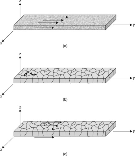
3.1 Illustration of three possible diffusion paths: (a) bulk diffusion through the volume or along the many grain boundaries in a polycrystalline line, (b) grain boundary diffusion through a columnar grain structure, and (c) surface diffusion along the top and bottom surfaces of a conductor line.
where the material is assumed to be deposited or depleted equally in all three directions, which is associated with bulk diffusion or diffusion along grain boundaries in a polycrystalline line,
where material is deposited or depleted equally in the two in-plane directions, which is associated with diffusion along grain boundaries in a columnar grain structure, and
where material is deposited or depleted in the thickness direction of the line, which is associated with diffusion along the top and bottom surfaces. It should also be noted that since the electromigration-induced mass flux leads to local changes in material volume, which is only associated with the diagonal elements of εem, it is reasonable to assume that the off-diagonal elements remain zero. With the addition of either equation [3.14] or [3.15] and choosing one of equation [3.16]–[3.18] or some other relationship between the electromigration-induced strain components, together with the governing equations [3.1] and [3.4]–[3.9] and initial and boundary conditions in equations [3.10]–[3.13], it is possible to solve for the electromigration-induced strain εem, the displacement field u, the elastic strains εe and the stress σ.
3.2.2 Analytical model
Korhonen et al. (1993) developed an analytic one-dimensional (1D) model that has been widely used. If we assume the interconnect line lies along the y direction and that the current density j and atomic flux J are directed along y, then substituting equation [3.1] into equation [3.4] becomes:
Furthermore, if the conductor line is constrained and the material in both the conductor and the surrounding layers is assumed to be linear elastic as given in equation [3.7], then there is a linear relationship between the stress ![]() (regardless of how it is defined, equations [3.14] or [3.15]) and the electromigration-induced unit volume change Δem, and thus,
(regardless of how it is defined, equations [3.14] or [3.15]) and the electromigration-induced unit volume change Δem, and thus,
where B is a constant and depends on the geometry and elastic properties of the conductor line and surrounding layers. Equations [3.19] and [3.20] then give the resulting 1D stress evolution equation
In order to use the above equation, an estimate of B is required. Korhonen et al. (1993) approximated the cross-section of the line as an elliptical inclusion in a homogeneous medium and applied the Eshelby theory of inclusions (Eshelby 1957) to estimate B. From the Eshelby inclusion theory, the inelastic, electromigration-induced strain in the inclusion is related to the resulting stress in the inclusion by
where K, I, and S = L− 1 are the fourth order Eshelby identity, and compliance tensors, and superscripts M and L indicate the surrounding medium and the conductor line, respectively. If the surrounding matrix material (passivation layer) is assumed to be isotropic with elastic modulus EM and Poisson’s ratio vM and the inclusion (conductor line) is treated as a face-centered-cubic material (e.g. aluminum or copper) with a strong < 111 > fiber texture and random in-plane texture (resulting in transversely isotropic symmetry about the z axis), then the above relationship becomes
where w and h are the width and thickness of the conductor line and SLij are the components of the compliance matrix for the line. By substituting in equation [3.16], [3.17], or [3.18], on the left hand side of [3.23], the system may be solved for σxx, σyy, and σZZ in terms of Δem, and the parameter B, relating ![]() and Δem, may then be determined. Although the above approximate analytic model provides some valuable insight into the evolution of stress in the line and the effect of different potential diffusion paths, it is not able to quantitatively capture the effect of the real geometry with multiple material layers and lines with non-elliptic cross-sections.
and Δem, may then be determined. Although the above approximate analytic model provides some valuable insight into the evolution of stress in the line and the effect of different potential diffusion paths, it is not able to quantitatively capture the effect of the real geometry with multiple material layers and lines with non-elliptic cross-sections.
3.2.3 Finite-element model
The finite-element method (FEM) allows for an accurate model of the geometry of the line and the consideration of multiple material layers. The Eshelby approximation of the cross-section derived above, for an elliptical inclusion in an infinite matrix, results in uniform stress and strain fields in the inclusion. However, if the inclusion is not elliptic, the stress and strain field in the inclusion is no longer uniform, and the finite element method is well-suited for determining these fields.
A finite-element formulation based on the governing equations presented in section 3.2.1 is as follows. Substituting equation [3.1] into equation [3.4] and taking the weak form yields:
for the conductor line where ![]() is an arbitrary weighting function, and the blocking boundary condition equation [3.11] has been used. We can also write the usual weak form for the equilibrium and linear elastic equations [3.6]–[3.9] over the domain V:
is an arbitrary weighting function, and the blocking boundary condition equation [3.11] has been used. We can also write the usual weak form for the equilibrium and linear elastic equations [3.6]–[3.9] over the domain V:
where v is an arbitrary vector valued weighting function that is zero on S2. The above two equations, together with the initial condition equation [3.10] and boundary condition equation [3.13], can be discretized with the finite-element method in space and a central difference in time for equation [3.24] and solved for Δem and u using a staggered approach. Specifically, letting Δt be the time step and n represent the current time increment, a discretesystem of equations results of the form:
where equation [3.26] represents the discrete form of equation [3.24] with coefficient matrix M, Δem represents a vector of nodal values of the electromigration-induced dilatational strain, and right-hand-side vector h depends on the current density j and stress ![]() at time tn. Equation [3.27] is the discrete form of equation [3.25] with coefficient matrix K, vector of nodal displacements u, and right-hand-side vector f depending on the electromigration induced strain εem and boundary traction
at time tn. Equation [3.27] is the discrete form of equation [3.25] with coefficient matrix K, vector of nodal displacements u, and right-hand-side vector f depending on the electromigration induced strain εem and boundary traction ![]() at time tn + 1. Thus, given information at the current time tn, equation [3.26] may be solved to update the electromigration-induced dilatational strain Δem at time tn + 1 = tn + Δt. Using this to define εn + 1em and given prescribed boundary tractions
at time tn + 1. Thus, given information at the current time tn, equation [3.26] may be solved to update the electromigration-induced dilatational strain Δem at time tn + 1 = tn + Δt. Using this to define εn + 1em and given prescribed boundary tractions ![]() , the displacement field can then be updated using equation [3.27] to time tn + 1, which may, in turn, be used to solve for the updated stress using Equations [3.7]–[3.9], and thus, updating
, the displacement field can then be updated using equation [3.27] to time tn + 1, which may, in turn, be used to solve for the updated stress using Equations [3.7]–[3.9], and thus, updating ![]() to be used in the next step in equation [3.26]. After sufficient time, a steady-state solution is reached where ∂Δem/∂t = 0 in equation [3.24] and
to be used in the next step in equation [3.26]. After sufficient time, a steady-state solution is reached where ∂Δem/∂t = 0 in equation [3.24] and
3.3 Experimental, modeling and simulation findings
This section shows how X-ray microbeam experiments together with modeling and simulation, using the methods described in section 3.2, may be used to infer information about the diffusion paths and driving stresses active during electromigration. Here, we focus on two X-ray microbeam experimental studies on aluminum (Al) conductor lines with very different observations.
3.3.1 Experiments
The two experiments considered are documented by Wang et al. (1998) and Zhang et al. (2008). Cross-sectional diagrams for the lines in each experiment are shown in Fig. 3.2a and 3.2b, and a transmission electron microscopy (TEM) image of the cross-section from the Zhang et al. (2008) investigation is shown in Fig. 3.2(c). In the study by Wang et al. (1998), the elastic strain component εzze was measured using energy-dispersive microbeam X-ray diffraction along the lengths of Al conductor lines that were 200 μm long, 10 μm wide, and 0.5 μm thick, with a 1.5 μm SiO2 passivation layer and a Si (100) substrate. There was also a 10 nm Ti/60 nm TiN shunt layer under the line, which is not shown in Fig. 3.2. The grain structure in the Al lines was columnar with average grain siLe roughly the same as the film thickness and had a strong < 111 > fiber texture, with the < 111 > crystal direction preferentially oriented along the z direction. The experimental temperature was 260 °C, and the current density was 1.4 × 10⁵ A cm− 2. In that experiment, the strain εzze was found to increase (become more tensile) linearly along the direction of electron flow. Zhang et al. (2008) measured both the elastic strain component εzze (using Bragg monochromatic diffraction) and all the components of the elastic, deviatoric strain tensor ![]() (using Laue white-beam diffraction) in separate experiments, throughout two Al conductor lines with nominally the same structure. The lines were approximately 30 μm long, 2.6 μm wide, and 0.75 μm thick, with a 0.7 μm SiO2 passivation layer and a Si (100) substrate. The grain structure consisted of polycrystalline (< 100 nm grain size), Ti-rich layers (probably mixture of Al and TiAl3 resulting from reaction of originally thin Ti liner layers with the Al line) above and below the central part of the line, each about 0.2 μm thick, and micrometer-size columnar Al grains of about 0.35 μm thickness in the central part of the line, as can be seen in Fig. 3.2c. The experimental temperature was 190 °C and the applied current was 30 mA corresponding to a current density of 2.1 × 10⁶ A cm− 2 if we assume the TiAl3 takes up approximately 30% of the cross-sectional area and the current only travels through the Al part of the line as the resistivity of TiAl3 is much higher than that of Al. In this experiment, the strain εzze was found to decrease (become more compressive) linearly along the direction of electron flow to a point and then became constant. Fig. 3.3 shows a comparison of the measured elastic strains εzze along the line lengths for the two experiments, showing the opposing trends.
(using Laue white-beam diffraction) in separate experiments, throughout two Al conductor lines with nominally the same structure. The lines were approximately 30 μm long, 2.6 μm wide, and 0.75 μm thick, with a 0.7 μm SiO2 passivation layer and a Si (100) substrate. The grain structure consisted of polycrystalline (< 100 nm grain size), Ti-rich layers (probably mixture of Al and TiAl3 resulting from reaction of originally thin Ti liner layers with the Al line) above and below the central part of the line, each about 0.2 μm thick, and micrometer-size columnar Al grains of about 0.35 μm thickness in the central part of the line, as can be seen in Fig. 3.2c. The experimental temperature was 190 °C and the applied current was 30 mA corresponding to a current density of 2.1 × 10⁶ A cm− 2 if we assume the TiAl3 takes up approximately 30% of the cross-sectional area and the current only travels through the Al part of the line as the resistivity of TiAl3 is much higher than that of Al. In this experiment, the strain εzze was found to decrease (become more compressive) linearly along the direction of electron flow to a point and then became constant. Fig. 3.3 shows a comparison of the measured elastic strains εzze along the line lengths for the two experiments, showing the opposing trends.
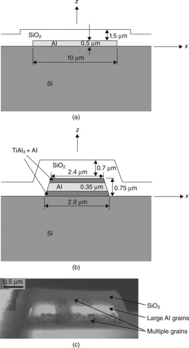
3.2 Schematic cross-sections for the two Al lines considered: (a) line investigated by Wang et al. (1998); (b) line by investigated Zhang et al. (2008); (c) TEM image of cross-section of line investigated by Zhang et al. (2008) showing small-grain polycrystalline layers on the top and bottom of the large grain Al line.
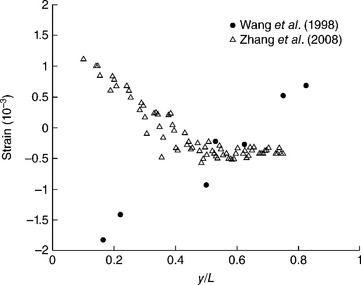
3.3 A comparison of the measured elastic strain εzze as a function of the normalized distance y/L along the line for the two Al lines considered here, where the electrons flow from left to right (current in –y direction).
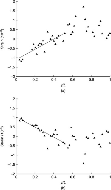
For the line investigated by Zhang et al. (2008), the measured deviatoric strain components, εyye∗ and εzze∗, are shown in Fig. 3.4(a) and 3.4(b). Since εxxe∗ = − (εyye∗ + εzze∗), εxxe∗ is not shown here. The shear strains were also found to be relatively small and are also not shown. As observed for the full, elastic strain component εzze in Fig. 3.3, a fairly linear trend is observed along the upstream end to about the middle of the line, but after this point, no clear trend is evident in the data, with a considerable amount of scatter appearing in the deviatoric data. In Zhang et al. (2008), the authors postulate that the passivation layer may have delaminated at the downstream end leading to a drop in the stress. They also suggested that plastic deformation or recrystallization at the downstream end may have led to an increase in scatter. Therefore, the focus is on the upstream end here, where linear fits to the data are shown in Fig. 3.4(a) and 3.4(b).
3.3.2 Eshelby and two-dimensional (2D) finite-element model findings
In order to start to understand the reason the two experiments described above exhibit opposite trends with regard to the elastic strain εzze, we compare the experimental results to results from two-dimensional (2D) cross-sectional models, where an inelastic, dilatational strain Δem prescribed in the line and each of the three scenarios for partitioning the strain given in equation [3.16]–[3.18] are considered.
Findings for the Zhang et al. (2008) experiment
Because we have measurements of all the components of the deviatoric, elastic strain as well as of the full, elastic strain component εzze for the Zhang et al. (2008) experiment, we first focus on that case. The approximate models used are shown in Fig. 3.5(a) and 3.5(b), where symmetry about the z axis is used in the finite-element model. Note that the Eshelby model approximates the line as an elliptic inclusion in an infinite matrix of the passivating material SiO2 and, thus, does not accurately represent the geometry nor the multiple layers of materials. The finite-element model here approximates the line geometry as rectangular rather than trapezoidal. The finite-element model also treats the Si substrate as effectively rigid, which from prior simulations has been found to be a reasonable approximation given the relatively large thickness of the substrate. Perfect bonding between the materials is also assumed (no relative sliding). The geometry shown in Fig. 3.5(b) is discretized into 1740 four-noded, bi-linear elements. The polycrys-talline SiO2 and the TiAl3 are treated as isotropic with elastic moduli and Poisson’s ratios of Es = 75 GPa and vs = 0.17 for the SiO2 and Et = 170 GPa and vt = 0.25 for the TiAl3. The Al is columnar and has a strong < 111 > texture, with the < 111 > direction preferentially oriented in the z direction, and the in-plane texture is fairly random. Thus, the Al may be treated as transversely isotropic with the axis of symmetry aligned with the z axis. The elastic stiffness parameters for the Al, computed from the single crystal properties at 190 °C, are C11 = C22 = 107.1 GPa, C33 = 108.7 GPa, C12 = 59.2 GPa, C13 = C23 = 57.5 GPa, C44 = C55 = 22.3 GPa, and C66 = (C11 – C12)/2 = 23.9 GPa.
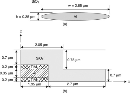
3.5 2D approximate models associated with the line cross-section in Fig. 3.2(b): (a) Eshelby model and (b) finite-element model geometry, where a symmetry boundary condition is taken about the z axis and the Si substrate is treated as rigid.
Because the current direction is perpendicular to the cross-section, at steady state, from equation [3.28], the stress gradient in the cross-section should be zero (![]() ). For the Eshelby model, this is automatically satisfied since the Eshelby model predicts a uniform stress field in the inclusion (conductor line) for a uniform inelastic, electromigration-induced strain in the inclusion, which may be found using equation [3.23]. In the finite-element model, an initially uniform electromigration-induced dilatational strain Δ0em is prescribed in the Al line and then equations [3.26] and [3.27] are solved until the distribution of Δem in the cross-section is found such that
). For the Eshelby model, this is automatically satisfied since the Eshelby model predicts a uniform stress field in the inclusion (conductor line) for a uniform inelastic, electromigration-induced strain in the inclusion, which may be found using equation [3.23]. In the finite-element model, an initially uniform electromigration-induced dilatational strain Δ0em is prescribed in the Al line and then equations [3.26] and [3.27] are solved until the distribution of Δem in the cross-section is found such that ![]() . Each definition of
. Each definition of ![]() given in equations [3.14] and [3.15] is considered as well as the three diffusion modes (i), (ii), and (iii) given in equation [3.16]–[3.18]. For the case where the stress
given in equations [3.14] and [3.15] is considered as well as the three diffusion modes (i), (ii), and (iii) given in equation [3.16]–[3.18]. For the case where the stress ![]() is taken to be the normal stress to the grain boundaries, equation [3.15], the corresponding stress normal to the grain boundaries for each assumed diffusion mode is defined as:
is taken to be the normal stress to the grain boundaries, equation [3.15], the corresponding stress normal to the grain boundaries for each assumed diffusion mode is defined as:
where grain boundaries are assumed to be equally distributed in all directions (note, this is the same as the hydrostatic stress equation [3.14]),
where the grains are assumed columnar and equi-axed, and
where the diffusion is assumed to be primarily along the top and bottom faces.
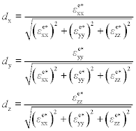
First, the measured deviatoric, elastic strain components εxxe∗, εyye∗, and εzze∗ in the conductor line are compared with those predicted for each model. Because the elastic strain components are predicted to be proportional to Δem, a direction associated with the normal strain components defined as:
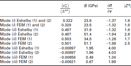
is used for comparison. Because the data is better for the upstream end, focus is on the upstream end where Δem < 0. For the experiment, the direction components are computed at several locations along the upstream end, and an average value is used. For the finite-element cases, the average elastic strains in the line cross-section are used in computing dx, dy, and dz. The experimental and simulation results for each case considered are given in Table 3.1. From Table 3.1, it can be seen that the mode (i) and mode (ii) models yield directions of the deviatoric, elastic strains that are nearly in the opposite direction from that observed in the experiment, whereas the mode (iii) simulations, which assume that material is depleted only in the thickness z direction, give strains that are nearly in the same direction as
Table 3.1
Comparison of the measured and predicted directions of the deviatoric, elastic strains. FEM (1) indicates finite-element model with gradient of the hydrostatic stress set to zero, and FEM (2) is when the gradient of the grain boundary stress is zero in the cross-section
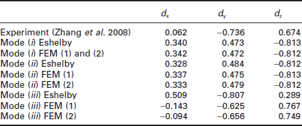
the experiment. From this we may conclude that the primary diffusion path for this experiment is probably through the interfaces between the columnar Al grains and the small TiAl3 grains. Of the mode (iii) simulations, the FEM (2) simulation gives the best result, which corresponds to the case where ![]() is defined according to equation [3.31], i.e. the case where the driving stress is assumed to be the normal stress relative to the top and bottom surfaces which are considered the primary diffusion paths. The angle between the experimental direction and the mode (iii) FEM (2) direction is 10.9°. The mode (iii) FEM (1) case gives a result that is nearly as good with an angle between the experiment and simulation of 14.5°. For the mode (iii) Eshelby case, the angle between the experiment and simulation is 34.3°, which is not as good quantitatively as the FEM simulations, but is still considerably closer than any of the mode (i) or mode (ii) simulations. Thus, the Eshelby approximation may be a good way to determine which is the dominant diffusion path, but a finite-element simulation is necessary for good quantitative agreement.
is defined according to equation [3.31], i.e. the case where the driving stress is assumed to be the normal stress relative to the top and bottom surfaces which are considered the primary diffusion paths. The angle between the experimental direction and the mode (iii) FEM (2) direction is 10.9°. The mode (iii) FEM (1) case gives a result that is nearly as good with an angle between the experiment and simulation of 14.5°. For the mode (iii) Eshelby case, the angle between the experiment and simulation is 34.3°, which is not as good quantitatively as the FEM simulations, but is still considerably closer than any of the mode (i) or mode (ii) simulations. Thus, the Eshelby approximation may be a good way to determine which is the dominant diffusion path, but a finite-element simulation is necessary for good quantitative agreement.
The finite-element simulation also allows for the computation of the nonuniform distribution through the cross-section of the electromigration-induced volumetric strain Δem, which is required to give a uniform ![]() in the cross-section. For the mode (iii) FEM (2) case, the normalized distribution of Δem is shown in Fig. 3.6(a) and 3.6(b). From these figures, we can see that more of the depleted (upstream, Δem < 0) or deposited (downstream, Δem > 0) material occurs towards the central part of the line (near x = 0), with much less material flowing to or from the edges (near x = ± 1.35 μm).
in the cross-section. For the mode (iii) FEM (2) case, the normalized distribution of Δem is shown in Fig. 3.6(a) and 3.6(b). From these figures, we can see that more of the depleted (upstream, Δem < 0) or deposited (downstream, Δem > 0) material occurs towards the central part of the line (near x = 0), with much less material flowing to or from the edges (near x = ± 1.35 μm).
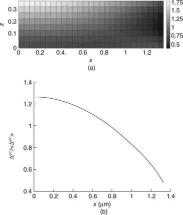
3.6 Distribution of the electromigration-induced volumetric strain Δem normalized by the average of this strain ![]() : (a) throughout the cross-section of the Al line (x and z in μm), and (b) from the middle to the edge of the line in the width direction averaged through the thickness.
: (a) throughout the cross-section of the Al line (x and z in μm), and (b) from the middle to the edge of the line in the width direction averaged through the thickness.
From the curve fits to the experimental data on the upstream end, shown in Fig. 3.4(a) and 3.4(b), the magnitude of the deviatoric, elastic strain, which was used to normalize the deviatoric elastic strain components in equation [3.32], may be computed along the line length on the upstream end. By multiplying the magnitude of the deviatoric strain by the direction predicted in the mode (iii) FEM (2) simulation (Table 3.1), the deviatoric, elastic strain components along the upstream end of the line may be computed, and these are shown in Fig. 3.7(a) and 3.7(b) with the experimental data. Furthermore, because the model predicts the elastic strains to be proportional to the electromigration-induced dilatational strain Δem, the average Δem may be determined along the length of the line for the upstream end, and from this, the full elastic strain εzze may be computed along the length for the upstream end from the simulation, which is shown compared with the experimental data in Fig. 3.8. The simulation prediction is slightly higher on average than the experimental trend, but in reasonable agreement.
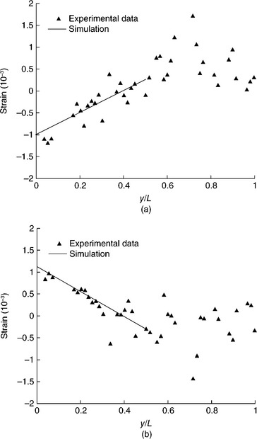
3.7 Comparison of the measured deviatoric, elastic strains along the line with that computed using the simulation direction for the components (a) εyye∗ and (b) εzze∗.
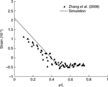
3.8 A comparison of the measured elastic, out-of-plane strain εzze∗ along the line with that computed from the simulation. The simulation predictions are based on the same linearly varying average Δem along the Al line length associated with the simulated strains in Figs. 3.7(a) and 3.7(b).
Lastly, we can use the simulation results to estimate |Z*|. From the finite element simulation result, we can determine the ratios ![]() and
and ![]() , where B is the parameter appearing in equation [3.21] and where
, where B is the parameter appearing in equation [3.21] and where
the angle brackets indicated averaged over the cross-section. Fitting the measured strain component εzze, shown in Fig. 3.3, to a straight line, the slope ![]() can be determined. Then the stress gradient may be determined from:
can be determined. Then the stress gradient may be determined from:
and used in equation [3.3] to find |Z*|. The predicted stress gradient along the line length is ![]() when the driving stress is taken as the interface stress given in equation [3.31] and
when the driving stress is taken as the interface stress given in equation [3.31] and ![]() when the driving stress is taken as the hydrostatic stress given in equation [3.14]. Using equation [3.3] and e = 1.602 × 10− 19 C, ρ = 4.54 × 10− 6 ohm cm for Al at 190 °C, Ω = 1.66 × 10− 23 cm3, and the current density estimated in section 3.3.1 of jy = − 2.1 × 10⁶ A cm− 2 (current flows in –y direction), |Z*| = 1.94 is obtained if the driving stress is the interface stress and |Z*| = 1.45 if it is the hydrostatic stress. The latter number is similar to other reported findings for |Z*| in Al conductor lines, which typically fall in the range of 1.2–1.6 (Blech and Tai 1977, Wang et al. 1998, Chiras and Clarke 2000).
when the driving stress is taken as the hydrostatic stress given in equation [3.14]. Using equation [3.3] and e = 1.602 × 10− 19 C, ρ = 4.54 × 10− 6 ohm cm for Al at 190 °C, Ω = 1.66 × 10− 23 cm3, and the current density estimated in section 3.3.1 of jy = − 2.1 × 10⁶ A cm− 2 (current flows in –y direction), |Z*| = 1.94 is obtained if the driving stress is the interface stress and |Z*| = 1.45 if it is the hydrostatic stress. The latter number is similar to other reported findings for |Z*| in Al conductor lines, which typically fall in the range of 1.2–1.6 (Blech and Tai 1977, Wang et al. 1998, Chiras and Clarke 2000).
Findings for the Wang et al. (1998) experiment
For the experimental results given in Wang et al. (1998), we only have one measured elastic strain component, εzze, as shown in Fig. 3.3. As in the previous case, 2D Eshelby and finite-element models were created for this experimental geometry, shown in Fig. 3.2(a), where now the Eshelby model is the same as shown in Fig. 3.5(a), but with w = 10 μm and h = 0.5 μm. The finite element model geometry is the same as the geometry in the schematic, Fig. 3.2(a), but, as in the previous analysis, without the Si substrate, which is treated as a rigid foundation, and modeling only half the geometry taking advantage of the symmetry about the z axis. The finite-element model was discretized with 3650 four-noded, bi-linear elements. The same properties for the Al and SiO2 as in the previous example are used.
From the 2D Eshelby and finite-element simulations, we can determine, for the different diffusion modes and assumed driving stress definitions, the stress and elastic strain fields in the line cross-section that result from a unit of electromigration-induced dilatational strain in the cross-section. Thus, as in the previous example, we can determine the ratios ![]() , and
, and ![]() and use this information together with the slope
and use this information together with the slope ![]() , determined from fitting the data in Fig. 3.3, to compute the stress gradient. Then,
, determined from fitting the data in Fig. 3.3, to compute the stress gradient. Then, ![]() is found using equation [3.3], where e and Ω are the same as used in the previous case, the current density is jy = − 1.4 × 10⁵ A cm− 2, and ρ = 5.5 × 10− 6 ohm-cm for Al at 260 °C. The model results are given in Table 3.2, where modes (i), (ii), and (iii), as before, refer to the considered diffusion modes described in equations [3.16]–[3.18], and (1) refers to considering the hydrostatic stress as the driving stress and (2) the grain boundary stress. From the results, we can first observe that mode (iii), where material is assumed to be deposited only in the z direction, is not a viable mode because it predicts a positive slope in the stress and thus, a negative |Z*|, which is not possible. Therefore, mode (iii) is ruled out as a possible diffusion mode. The remaining cases all predict values of |Z*| between 1.7 and 2.6. In Wang et al. (1998), the likely primary diffusion path was identified as being along the columnar grain boundaries with material deposited equally in x and y, the mode (ii) assumption. Assuming an equi-biaxial stress in the film, and assuming the hydrostatic stress as the driving stress, they found |Z*| = 1.6, which is close to values of 1.8 and 1.7 found here with the mode (ii) Eshelby and finite-element simulations, respectively. It is interesting to note that the Eshelby and the finite element simulations give very similar results for this particular cross-section geometry, where the line is relatively wide and only the Al line and the SiO2 passivation layer are considered in the models.
is found using equation [3.3], where e and Ω are the same as used in the previous case, the current density is jy = − 1.4 × 10⁵ A cm− 2, and ρ = 5.5 × 10− 6 ohm-cm for Al at 260 °C. The model results are given in Table 3.2, where modes (i), (ii), and (iii), as before, refer to the considered diffusion modes described in equations [3.16]–[3.18], and (1) refers to considering the hydrostatic stress as the driving stress and (2) the grain boundary stress. From the results, we can first observe that mode (iii), where material is assumed to be deposited only in the z direction, is not a viable mode because it predicts a positive slope in the stress and thus, a negative |Z*|, which is not possible. Therefore, mode (iii) is ruled out as a possible diffusion mode. The remaining cases all predict values of |Z*| between 1.7 and 2.6. In Wang et al. (1998), the likely primary diffusion path was identified as being along the columnar grain boundaries with material deposited equally in x and y, the mode (ii) assumption. Assuming an equi-biaxial stress in the film, and assuming the hydrostatic stress as the driving stress, they found |Z*| = 1.6, which is close to values of 1.8 and 1.7 found here with the mode (ii) Eshelby and finite-element simulations, respectively. It is interesting to note that the Eshelby and the finite element simulations give very similar results for this particular cross-section geometry, where the line is relatively wide and only the Al line and the SiO2 passivation layer are considered in the models.
3.4 Conclusions
Modeling and simulation coupled with X-ray microbeam measurement of elastic strains in conductor lines can be used to resolve some of the challenging questions regarding the physics of electromigration. Three key questions discussed here are:
1. How does the diffusing mass arrange itself and what does this imply about the dominant diffusion paths?
2. What is the appropriate driving stress for electromigration, hydrostatic or grain boundary/interface stress?
For the two Al conductor line geometries considered here, the diffusing mass was determined to arrange itself very differently, with the material deposition/depletion in the line thickness (z) for the Zhang et al. (2008) case and in the width and length (x and y) for the Wang et al. (1998) case. From these results, it may be concluded that for the Zhang et al. (2008) case, the primary diffusion path is probably along the top and bottom interfaces between the large columnar Al grains and the small polycrystalline TiAl3 layers, whereas for the Wang et al. (1998) case, where the line is much wider with more Al columnar grain boundaries and much thinner TiAl3 layers, it is probable that the columnar grain boundaries were the primary diffusion path. As far as the appropriate driving stress, the results are not as clear. The Laue white-beam microdiffraction measurements, where all the components of the deviatoric, elastic strain are measured, provides sufficient data to investigate the driving stress by comparing the measured and computed directions of the deviatoric, elastic strains. From the Zhang et al. (2008) data, when the driving stress was assumed to be the stress normal to the primary diffusion interfaces, the computed direction of the deviatoric, elastic strain was slightly closer to the measured direction than that found when using the hydrostatic stress as the driving stress. More studies would be needed to make a conclusive statement. When the driving stress was assumed to be the grain boundary or interface stress normal to the primary diffusing paths, |Z*| was found to be 1.94 from the Zhang et al. (2008) data and 2.5 from the Wang et al. (1998) data, and when the hydrostatic stress was used as the driving stress in the analysis, |Z*| was found to be 1.45 from the Zhang et al. (2008) data and 1.7 from the Wang et al. (1998) data. Because the primary diffusion paths were different types of material interfaces for the two cases considered, the value of |Z*| may not be the same. Additional studies are needed to clarify the question of the driving stress and to pin down |Z*|. The approach described here can be used to answer these questions, not only in aluminum interconnects, but also in copper. Three-dimensional finite element analyses could also provide additional insight, in particular about the validity of the plane strain assumption assumed here and time dependent behavior along the line direction.
3.5 Acknowledgments
This material is based upon work supported by the National Science Foundation under Grant No. DMR-0312189. The X-ray diffraction experiments were carried out on several beamlines at the National Synchrotron Light Source, Brookhaven National Laboratory, and on beamline 34-ID at the Advanced Photon Source, Argonne National Laboratory, both of which are supported by the United States Department of Energy.
3.6 References
Blech, I.A., Herring, C. Stress generation by electromigration. Appl Phys Lett. 1976; 29:131–133.
Blech, I.A., Tai, K.L. Measurement of stress gradients generated by electromigration. Appl Phys Lett. 1977; 30:387–389.
Cargill, G.S., III., Moyer, L.E., Wang, G., Zhang, H., Hu, C.K., Yang, W., Larson, B.C., Ice, G.E. Thermal and electromigration-induced strains in polycrystalline films and conductor lines: X-ray microbeam measurements and analysis. AIP Conf Proc. 2006; 816:303–309.
Chiras, S., Clarke, D.R. Dielectric cracking produced by electromigration in microelectronic interconnects. J Appl Phys. 2000; 88:6302–6312.
Clement, J.J., Thompson, C.V. Modeling electromigration-induced stress evolution in confined metal lines. J Appl Phys. 1995; 78:900–904.
Eshelby, J.D. The determination of the elastic field of an ellipsoidal inclusion and related problems. Proc R Soc Lond A. 1957; 241:376–396.
Gleixner, R.J., Nix, W.D. A physically based model of electromigration and stress-induced void formation in microelectronic interconnects. J Appl Phys. 1999; 86:1932–1944.
Hau-Riege, S.P., Thompson, C.V. The effect of the mechanical properties of the confinement material on EM in metallic interconnects. J Mater Res. 2000; 15:1797–1802.
Hu, C.K., Rosenberg, R., Lee, K.Y. Electromigration path in Cu thin-film lines. Appl Phys Lett. 1999; 74:2945–2947.
Korhonen, M.A., Borgesen, P., Tu, K.N., Li, C.Y. Stress evolution due to electromigration in confined metal lines. J Appl Phys. 1993; 73:3790–3799.
Ma, A., Chiras, S., Clarke, D.R., Suo, Z. High-resolution determination of the stress in individual interconnect lines and the variation due to electromigration. J Appl Phys. 1995; 78:1614–1622.
Nucci, J.A., Krämer, S., Arzt, E., Volkert, C.A. Local strains measured in Al lines during thermal cycling and electromigration using convergent-beam electron diffraction. J Mater Res. 2005; 20:1851–1859.
Park, Y.J., Andleigh, V.K., Thompson, C.V. Simulations of stress evolution and the current density scaling of electromigration-induced failure times in pure and alloyed interconnects. J Appl Phys. 1999; 85:3546–3555.
Penney, R.V. Current-induced mass transport aluminum. J Phys Chem Solids. 1964; 25:335–345.
Povirk, G.L. Numerical simulations of electromigration and stress-driven diffusion in polycrystalline interconnects. Mater Res Soc Symp Proc. 1997; 473:337–342.
Sarychev, M.E., Zhitnikov, Y.V., Borucki, L., Liu, C.L., Makhviladze, T. A new, general model for mechanical stress evolution during electromigration. Thin Solid Films. 2000; 365:211–218.
Solak, H.H., Vladimirsky, Y., Cerrina, F., Lai, B., Yun, W., Cai, Z., Ilinski, P., Legnini, D., Rodrigues, W. Measurement of strain in Al-Cu interconnect lines with X-ray microdiffraction. J Appl Phys. 1999; 86:884–890.
Spolenak, R., Barr, D.L., Gross, M.E., Evans-Lutterodt, K., Brown, W.L., Tamura, N., MacDowell, A.A., Celestre, R.S., Padmore, H.A., Valek, B.C., Bravman, J.C., Flinn, P., Marieb, T., Keller, R.R., Batterman, B.W., Patel, J.R. Microtexture and strain in electroplated copper interconnects. Mater Res Soc Symp Proc. 2001; 612:1–7.
Tamura, N., Celestre, R.S., MacDowell, A.A., Padmore, H.A., Spolenak, R., Valek, B.C., Chang, N.M., Manceau, A., Patel, J.R. Submicron X-ray diffraction and its applications to problems in materials and environmental science. Rev Sci Instrum. 2002; 73:1369–1372.
Tamura, N., Valek, B.C., Spolenak, R., MacDowell, A.A., Celestre, R.S., Padmore, H.A., Brown, W.L., Marieb, T., Bravman, J.C., Batterman, B.W., Patel, J.R. Grain orientation and strain measurements in sub-micron wide passivated individual aluminum test structures. Mater Res Soc Symp Proc. 2001; 612:1–6.
Valek, B.C., Bravman, J.C., Tamura, N., MacDowell, A.A., Celestre, R.S., Padmore, H.A., Spolenak, R., Brown, W.L., Batterman, B.W., Patel, J.R. Electromigration-induced plastic deformation in passivated metal lines. Appl Phys Lett. 2002; 81:4168–4170.
Wang, P.C., Cargill, G.S., III., Noyan, I.C., Hu, C.K. Electromigration-induced stress in aluminum conductor lines measured by X-ray microdiffraction. Appl Phys Lett. 1998; 72:1296–1298.
Zhang, H., Cargill, G.S., III., Ge, Y., Maniatty, A.M., Liu, W. Strain evolution in Al conductor lines during electromigration. J Appl Phys. 2008; 104:123533.


