The evolution of microstructure in copper interconnects during electromigration
Abstract:
The key concepts and experimental techniques in investigating the evolution of microstructure in Cu interconnects during electromigration are discussed and some of the fundamental changes in the microstructure during electromigration are described. The practical implications of such microstructural changes in relation to electromigration degradation mechanisms and lifetime measurement methodology are assessed.
6.1 Introduction
Studies of the evolution of microstructure during electromigration in metallic interconnects and especially the dependence on geometries, materials and fabrication methodologies of the interconnect schemes are of the utmost importance not only technologically but also scientifically for two related reasons. First, how the microstructure evolves during electromigration can provide insights into the fundamental understanding of materials degradation mechanisms that would not otherwise be revealed by ex situ observations (Chen et al., 2007; D’Haen et al., 1999; Tong et al., 2009). Such understanding is crucial in order to control electromigration damage and thus, to a large extent, the reliability of the metallic interconnects.
Second, the current and future technological drive to smaller and smaller dimensions in the advanced interconnect schemes (Ho et al., 2010; McPherson, 2001) and even across to the whole new dimension completely as in three-dimensional (3D) interconnects (Lu et al., 2009; Saraswat, 2010) and the introduction of novel materials and fabrication processes at unprecedented rates have led us into uncharted territories in terms of scientific understanding and could very well lead to new reliability phenomena (McPherson, 2006). Studying how the microstructure evolves during electromigration in these new regimes of materials in which the length scales are near or in the order of their microstructural features (such as grain boundary, twin boundary, dislocation sub-structure, dislocation confinements) is critical if we are to control these new failure mechanisms and reliability phenomena. Plastic behavior in nanoscale metallic materials has already been found to deviate starkly from the classical mechanics of large-scale metallic materials (Budiman et al., 2008; 2011; Feng et al., 2008; Lee et al., 2010; Nix et al, 2007). Plasticity, in particular, thus has a significant role in the evolution of microstructure in the nanoscale metallic interconnect schemes during any thermal/electrical/mechanical loading of the materials and is therefore the subject of much of this chapter.
In 6.2, the experimental observations of the evolution of microstructure in Cu interconnects during electromigration are discussed, in particular the role that plasticity plays. Particular materials characterization techniques that enable these in situ observations are described. Section 6.3 covers the particular effects of fabrication processes and initial microstructure of the copper interconnect materials on its evolution and the following degradation mechanisms during electromigration especially in its accelerated or test conditions. In 6.4, the implications of these effects on the reliability of current and future generations of advanced copper interconnect schemes are discussed.
6.2 Copper microstructure evolution during electromigration
Metal thin films patterned into submicrometer and even nanometer-scale conductor lines comprise the communication network of all integrated circuits. When the electrical current density running through these increasingly smaller and smaller wires becomes large enough (MA cm−2), atoms start to migrate, causing voids and hillocks to form under certain circumstances and eventually resulting in the final catastrophic failure of the device. Valek et al. (2002; 2003) first discovered a very unusual mode of plastic deformation occurring at an early stage of electromigration in Al interconnects. The deformation geometry introduces dislocation lines predominantly in the direction of electron flow, and thus may provide additional easy paths for the transport of point defects. Because these findings occur long before any observable voids or hillocks are formed, they may have a direct bearing on the final catastrophic events of failure of the device.
Valek et al. (2002; 2003) showed the unique and powerful capability of synchrotron X-ray microdiffraction. Utilizing a submicrometer-focused polychromatic synchrotron X-ray beam developed in the Beamline 7.3.3 (now Beamline 12.3.2) at the Advanced Light Source (ALS), Berkeley Lab, the technique proved advantageous as a local probe of mechanical behaviors, and in particular plastic deformation in small-scale devices. Furthermore, with this facility, in situ electromigration experiments can now be conducted, which are almost impossible with other characterization techniques. This capability enables us to investigate the evolution of the structure of the crystals as they deform owing to the enormous wind force of electrons moving from one end of the interconnect line to the other. This is an important piece of information for the fundamental understanding of electromigration degradation processes in metallic interconnects.
6.2.1 Synchrotron-based scanning X-ray submicron diffraction (μSXRD)
Synchrotron-based scanning X-ray submicron diffraction, also known as μSXRD (Budiman, 2008; Tamura et al., 2003; Valek et al., 2003), is essentially an X-ray diffraction (XRD) technique. Its unique feature stems from the fact that the X-ray beam comes from a synchrotron source, which is orders of magnitude brighter than a laboratory X-ray source, and which can be focused into a submicrometer spot size (Tamura et al., 2003). This capability enables characterization of materials and their mechanical properties at high (submicrometer) spatial resolution. The polychromatic characteristic of the synchrotron radiation makes it sensitive to local lattice curvature or rotation in the crystals under consideration (Budiman, 2008).
Traditional X-ray diffraction is a technique that has been used for almost a century for elucidating the structure of materials on the macroscopic scales (0.1–10 mm). As modern electronics, photonics and even biological devices are increasingly made on a smaller and smaller scale (submicrometer and nanometer scales), a thorough understanding of the materials structure–properties–performance relationship at such length scales (0.1–10 μm) has become critical, and thus the need for high spatial resolution XRD. With the recent availability of bright third generation synchrotron sources and recent advances in X-ray focusing optics, it is now practical to develop an X-ray microdiffraction technique and apply it to characterize materials at such small scales.
The Advanced Light Source (ALS) at the Ernest Orlando Lawrence Berkeley National Laboratory in Berkeley, CA, is a third-generation synchrotron radiation source. It is well known as one of the brightest available sources of extreme ultraviolet and soft X-ray radiation in the world. A wide range of scientific activity, ranging from protein crystallography and semiconductor physics, to the pioneering technology development of the extreme ultraviolet (EUV) lithography technique critical to the continuing scaling of the microelectronics chips, have been supported by the ALS. In order to provide a wide range of energy spectra, the ALS uses a bend magnet insertion device, as well as superbend (superconducting bend magnet) sources. The X-ray microdiffraction beamline described here is located at bend magnet Beamline 7.3.3 (now Beamline 12.3.2) of the ALS. The beamline provides an extremely bright X-ray beam with a spectral range of approximately 5–20 keV.
Because this synchrotron-based technique is what enables the in situ observations of the Cu microstructure evolution during electromigration, this technique is discussed in further detail in the following subsection.
Beamline components and layout
Figure 6.1 shows the schematic layout of the X-ray microdiffraction beamline. The X-ray beam from a bending magnet source (1.9 GeV, 400 mA, 250 μm FWHM × 40 μm FWHM, up to 3 × 0.2 mrad divergence in the horizontal and vertical, respectively) is 1 : 1 refocused at the entrance of the hutch by a 700 mm long platinum-coated silicon toroidal mirror operating at a grazing angle of 5.4 mrad (Tamura et al., 2003; Valek et al., 2003). Among few suitable methods for focusing high brightness white-beam X-rays, Kirkpatrick-Baez (KB) mirror pairs has been chosen for producing our X-ray focused beam in the Beamline 7.3.3 (now Beamline 12.3.2) as it is the only focusing solution to combine both achromaticity and high efficiency (Tamura et al., 2003). The principle of these KB mirrors has been described in detail elsewhere (MacDowell et al., 2001). These KB mirrors focus the X-ray synchrotron beam into a submicrometer spot size (0.5 μm × 0.5 μm FWHM). Acting as an adjustable size source for the KB demagnifying optics inside the hutch are the water-cooled tungsten slits at the entrance of the hutch. In this way spot size can be traded for flux. As white-beam has been mostly used in the studies described in the rest of this chapter, the 4-crystal monochromator in Fig. 6.1 is not utilized.
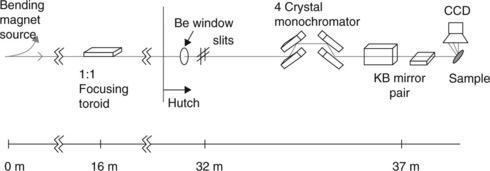
6.1 Schematic layout of the Beamline 7.3.3 (now Beamline 12.3.2) at the Advanced Light Source (ALS), Berkeley Lab.
As shown in Fig. 6.1, after the X-ray white-beam is focused by the KB mirrors, there remain two main components: the sample stage, and the large area charge-coupled device (CCD) X-ray detector, both of which are mounted on a goniometer as shown in Fig. 6.2. The sample under consideration would sit on a fine XY piezoelectric stage (range of +/− 50 μm), which is mounted on a coarse XYZ Huber stage (range of +/− 5 mm in XY and +/− 10 mm in Z) as shown in Fig. 6.3. The sample can also be mounted on a heating stage for experiments requiring temperatures up to 600 °C.
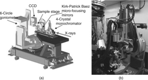
6.2 Experimental endstation for Beamline 7.3.3 (now Beamline 12.3.2) at the ALS: (a) the schematic of the engineering model, and (b) picture of the actual endstation. (courtesy of Tamura et al., 2003)
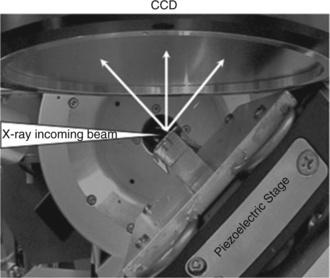
6.3 Side view of our typical experimental setup with the two-dimensional (2D) CCD detector on top and the sample mounted in a 45° reflective geometry; X-ray incoming beam and diffracted beams are shown as white arrows, and the sample movement is precisely controlled by the piezoelectric stage.
The diffraction patterns are collected with a MAR133 X-ray CCD (active area of 133 mm × 133 mm). The sample is usually mounted in a 45° reflective geometry as illustrated in Fig. 6.3, with the CCD detector on a vertical slide at a distance of approximately 50 mm from the sample area illuminated by the beam. This sample–CCD distance is optimized to give the maximum total number of reflections at a reasonable angular resolution. When illuminated with a white beam of 5–20 keV energy range, a (111) oriented Al grain, for example, gives a total of ~18 reflections, at an angular resolution of 0.01° (MacDowell et al., 2001).
Compared with electron microscopy techniques, X-rays offer the advantages of characterization of buried grains under overlying cap layers and multilayered films without the need of any sample preparation/destruction. In situ measurement under a variety of different conditions (in air, liquid, gas, vacuum, at different temperatures and pressures) thus becomes a possibility and opens opportunities for many experimental applications. The lack of sample preparation is especially important since the sample stress state can be greatly affected by any preparation processes.
White-beam μSXRD as local plasticity probe
The unique capability of the technique as a local plasticity probe stems from the polychromatic (white-beam) characteristics of the synchrotron radiation. This is what makes it sensitive with respect to local lattice curvature or rotation in the crystals under consideration. Because plasticity, especially in its special configurations in the forms of geometrically-necessary dislocations (GNDs) (Gao and Huang, 2003), is directly related to the local lattice curvature (Budiman, 2008), this technique has been most suitable for probing and studying the evolution of microstructure of materials especially in terms of its plasticity. This sensitivity to local lattice curvature is related to the continuous range of wavelengths in a white X-ray beam, allowing Bragg’s Law (Bragg, 1913) to be satisfied even when the lattice is locally rotated or bent, resulting in the observation of streaked Laue spots.
White-beam Laue diffraction is a standard crystallographic method used to determine crystal orientation without rotation of the sample. Laue diffraction is usually rarely used to measure strain because the precision of most Laue instruments is low compared with modern diffractometers, and because the unit cell volume cannot be determined with a standard Laue measurement. Nevertheless, with suitable instrumentation, such as that used in the experimental setting described above, precise determination of crystal orientation and distortional strain is possible. Laue diffraction might even be further extended by measuring the energy of one or more reflections to determine the full strain tensor in polycrystalline samples.
A single white-beam Laue diffraction pattern as shown in Fig. 6.4 contains a wealth of information about crystallographic orientation (Fig. 6.4a), deviatoric stresses/strains (Fig. 6.4b), and dislocation structure/density (Fig. 6.4c) as well as crystal rotation (Fig. 6.4d) in each individual crystal of the typically polycrystalline samples. Figure 6.4 shows features in a Laue diffraction pattern and the associated structural and mechanical information that they contain about the materials/sample. The shape of the Laue peak provides information about plastic deformation in the crystal (Fig. 6.4c), especially the one involving GNDs. The change in the absolute position of the Laue peak gives us the rotational deformation of the crystal body (Fig. 6.4d).
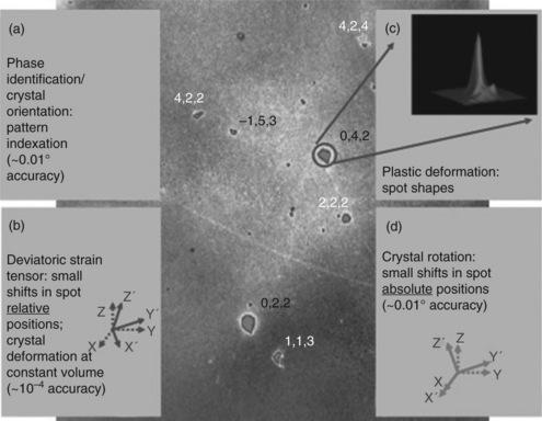
6.4 A single white-beam CCD image consisting of multiple sets of Laue diffraction peaks from a Cu polycrystalline sample.
A typical X-ray microdiffraction scanning of a sample usually yields hundreds to a few thousands of these Laue diffraction patterns. Without a set of software tools that can rapidly analyze the multiple Laue patterns contained in each of the CCD images produced by our experiments, the abundant raw data could not translate to meaningful information about the materials. A computer automated technique developed for crystallographic indexing, orientation, and strain determinations of grains in thin film samples (Chung and Ice, 1999; Ice and Larson, 2000; Tamura et al., 1999; 2002) was used, and a custom-made software was developed, namely X-ray microdiffraction analysis software (XMAS) (Tamura et al., 2002). It is based on an algorithm first described by Chung and Ice (1999).
Crystal bending, polygonization and rotation
In traditional XRD experiments, a peak at a certain angle θ means a particular (hkl) plane is detected, i.e. the particular angle θ, interplanar distance dhkl and wavelength λCu,kα (for instance) conspire such as to satisfy Bragg’s Law (Bragg, 1913):
Using this methodology, only elastic deformation of crystal can be determined, where strain can simply be computed from the difference of interplanar distances between atomic planes, before and after the deformation. In contrast, plastic deformation may involve curved and polygonized crystal planes, such as shown in Fig. 6.5. In such configurations, a particular crystal plane (with a fixed dhkl interplanar distance) may have a range of values of θ angle. This lattice curvature information is lost in traditional XRD (using a single wavelength and no tilt). However, using a white-beam X-ray, which has a range of wavelengths, Bragg’s law can still be satisfied even though the θ angle varies. This means that with white-beam, a presence of lattice curvature can still be detected and even measured.
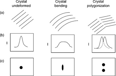
6.5 (a) Schematic diagrams of a set of crystal planes in their undeformed, bent/curved and polygonized states; (b) the expected Laue diffraction peaks corresponding to each of the crystal states; in intensity scanning over angle consisting of the Bragg angle/s; and (c) in CCD detector space. (courtesy of Spolenak et al., 2002)
For a curved crystal plane (crystal bending), a broadened Laue diffraction peak in a certain direction is observed (Fig. 6.5) instead of a single, sharp, rounded peak typical of an undeformed crystal plane. The Laue peak broadening (also called ‘peak streaking’) is continuous, representing the continuum of θ values involved in the curved crystal. Crystal polygonization, in contrast, involves multiple, discreet peaks coming from slightly misoriented sub-crystal structures (such as shown in Fig. 6.5). Such polygonization often occurs following bending of the crystal where more and more dislocations pile up, and thus become unstable with respect to glide and eventually climb to form a low-angle boundary (Cahn, 1949; Gilman, 1955; Hibbard and Dunn, 1956; Patel, 1958).
This is the unique capability of our white-beam X-ray diffraction technique. Using this white-beam methodology, we can start to directly and quantitatively study the evolution of microstructure of crystalline materials especially in terms of its plasticity. This technique is especially sensitive towards crystal bending or polygonization in their simplest geometries, where a net density of parallel like-sign GNDs is formed.
Furthermore, in traditional XRD, when a body of crystal rotates, the angle θ changes and, without rotating the sample, equation [6.1] can no longer be satisfied. In contrast, using a white-beam X-ray, another wavelength is available to satisfy the diffraction condition, and thus give a constructive interference in the diffracted intensity (a Laue diffraction peak) instead on a slightly different position in the CCD camera, such as shown in Fig. 6.6. In other words, a crystal rotation would appear as a shift in the absolute positions of each of the Laue peaks belonging to the same crystal (it is to be noted that a change in the relative position of the Laue peaks, relative to other peaks belonging to the same crystal, in contrast, does not mean crystal rotation, but instead, shear deformation or in other words, deviatoric strains).
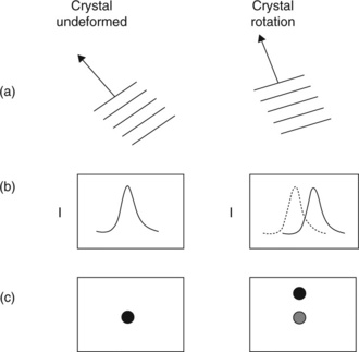
6.6 (a) Schematic diagrams of two bodies of crystal in their undeformed/unrotated and rotated states; (b) the expected Laue diffraction peaks corresponding to each state, in intensity scanning over angle consisting of the Bragg angle (there is a shift in the absolute angular position of the peak); and (c) in CCD detector space (again, a shift in the position of the peak on the CCD detector space).
6.2.2 Electromigration-induced microstructural changes in copper interconnects
The μ-SXRD technique using focused synchrotron radiation white-beam developed in the Beamline 7.3.3 (now Beamline 12.3.2) at the ALS Berkeley Lab has been used to study the microstructural evolution at the granular level of Cu polycrystalline lines during electromigration (Budiman et al., 2004; 2006a; 2006b). An unexpected mode of plastic deformation was observed in damascene Cu interconnect test structures during an in situ electromigration experiment and before the onset of visible microstructural damage (such as void and hillock formation). We show here, using this synchrotron technique, that the extent of this electromigration-induced plasticity is dependent on the line width. In wide lines, plastic deformation manifests itself as grain bending and the formation of subgrain structures, whereas only grain rotation is observed in the narrower lines. This electromigration-induced plasticity tends to occur in large grains spanning across the width of the Cu lines in the form of grain bending and polygonization, whereas smaller grains tend to just rotate.
Furthermore, we observe that the bending axis of this plastic deformation coincides with one of the < 112 > line directions of the known slip systems for FCC crystal, and that it is always very close (within a few degrees) to the direction of the electron flow in the lines. This finding suggests a correlation of the proximity of a < 112 > line direction to the direction of electron flow with the occurrence of plastic behavior. This deformation geometry leads us to conclude that dislocations introduced by plastic flow lie pre-dominantly in the direction of electron flow and may provide additional easy paths for the transport of point defects. Because these deformations occur long before any observable voids or hillocks are formed, they may have a direct bearing on the final failure stages of electromigration.
The synchrotron technique of scanning white-beam X-ray microdiffraction in particular has enabled these in situ observations (Budiman et al., 2004; 2006a; 2006b). Other in situ microstructure characterization studies have given valuable insights on the degradation mechanism of electromigration in Cu lines (Meyer et al., 2002; Vairagar et al., 2004; Doan et al., 2000). To complement these studies, the high-brilliance synchrotron radiation used here allows in situ studies of crystal lattice rotation and its evolution during electromigration. This is an important piece of information that contributes to the fundamental understanding of electromigration degradation mechanisms. In the following subsection, the experimental details of the investigation will be discussed.
Experimental
The interconnect test structure used here is an electroplated Cu damascene line manufactured by Intel Corporation (Budiman et al., 2004; 2006a; 2006b). The test line has dimensions of 70 μm in length and approximately 1 μm in thickness, with two different widths of 1.6 and 0.6 μm. The lines are embedded in a SiO2/SiOF interlayer dielectric film. The structure is then passivated with nitride and polyimide. The interconnect lines were produced by the damascene technique in which the copper is plated out into open channels and then mechanically polished to the desired thickness. Both vias at either end of the line connect to a lower metallization level, which, in turn, connects to unpassivated bond pads which are used for electrical connection. A schematic diagram of these structures with line dimensions is shown in Fig. 6.7.
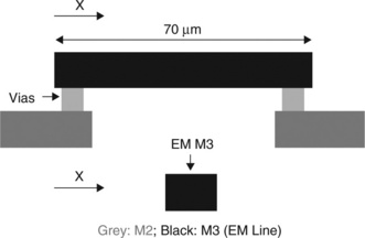
6.7 The schematic diagram of the Cu electomigration test structures manufactured by Intel Corporation (Budiman et al., 2004; 2006a; 2006b).
The white-beam X-ray microdiffraction experiment was performed on Beamline 7.3.3 (now Beamline 12.3.2) at the Advanced Light Source, Berkeley, CA. The electromigration test was conducted first at 300 °C. Current and voltage were monitored at 10 s increments. The sample (width 1.6 μm) was scanned in 0.5 μm steps, 10 steps across the width of the line and 160 steps along the length of the line, for a total of 1600 CCD frames collected as illustrated in Fig. 6.8. A complete set of CCD frames takes about 6 to 7 h to collect. The exposure time was 4 s plus about 10 s of electronic readout time for each frame. In this manner the Laue pattern and information regarding plastic deformation for each grain in the sample was collected for each time step during the experiment. The current was ramped up to 50 mA (j = 3.1 MA cm−2) over the course of 96 h, and then set at that value for the rest of the test.
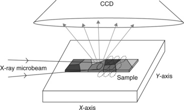
6.8 Schematic diagram of a scanning white beam X-ray microdiffraction experiment. The incoming X-ray beam illuminates a volume that may consist of more than one crystal and the diffracted beams from each discrete volume of the sample, followed by the next volume in a discrete-step scanning mode. (courtesy of Valek, 2003)
The second group of tests was conducted at a higher temperature, 360 °C, for reasons that are discussed later in this chapter. The narrow sample (0.6 μm) was scanned in the same manner as above, except that the current ramp up was ≤ 20 mA (j = 3.3 MA cm−2) over the course of 96 h, and then set at that value for the rest of the test.
A rough elemental map of the sample has first to be created using scanning X-ray fluorescence, so that the region of interest can be more precisely pinpointed. For the samples in our experiments, we typically used copper, titanium, platinum and gold fluorescence signals. Subsequently, the area of interest can be precisely located by using the piezoelectric positioning stage. A typical big-picture elemental map is shown in Fig. 6.9, from which the exact co-ordinates can be determined for a more precise X-ray microdiffraction scan, and Laue patterns can thus be collected from each discrete area in the coordinates of interest.
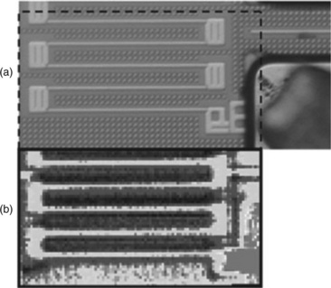
6.9 Examples of fluorescence mapping for locating the sample’s overall picture: (a) a series of horizontal copper interconnect lines (Budiman et al., 2004; 2006a; 2006b) and (b) the corresponding fluorescence mapping using copper’s characteristic radiation wavelength (mid-gray = high intensity of copper fluorescence characteristic radiation, light gray = medium, dark gray = low). A 0.5 μm step size in x and y was used.
Initial microstructure
We first describe the microstructure of the wide (1.6 μm) damascene Cu test structures. The grain out-of-plane and in-plane orientations in these lines as determined by white-beam X-ray microdiffraction through the passivation layer are shown in Fig. 6.10a and 6.10b, respectively.
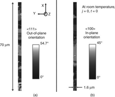
6.10 Grain orientation mapping of the wide (1.6 μm) passivated Cu lines using synchrotron-based X-ray microdiffraction with a focused beam (FWHM ~ 0.8 μm): (a) crystal < 111 > out-of-plane orientation; (b) crystal < 100 > in-plane orientation (Budiman et al., 2004; 2006a; 2006b).
Figure 6.10a shows all grains along the interconnect line with the < 111 > direction of the individual grains varying from 0° (normal to sample surface) to 54.7° away from the normal of the sample surface. In other words, the darker the color of the grains, the closer those grains are to having < 111 > out-of-plane orientation, and the lighter the color, the further away they are from having < 111 > out-of-plane orientation. It is evident from Fig. 6.10a that Cu grains in the damascene interconnect test structures were found in a wide range of out-of-plane orientations. This is consistent with observations on industry-relevant Cu interconnect test structures (Lingk et al., 1999a; 1999b; 2000). Only a few of the grains (black-colored in Fig. 6.10a) are actually < 111 > grains, some others are quite close (dark) to being < 111 > grains, whereas many others are far off (light white to colored), even approaching < 100>-out-of-plane-oriented grains (54.7° off).
Most of the grains are large grains spanning across the width of the line. It is reasonable to suspect that the Cu grains here extend through the whole thickness of the line, making it a bamboo structure. This is true along the line, however, in areas close to the via regions, grains are smaller, and more likely to be three-dimensional in structure (not bamboo). This trend has been reported (Besser et al., 2001; Doan et al, 2000; Lingk et al, 1999a; 1999b; 2000), where the wider Cu damascene lines were shown to be closer to the behavior of Cu blanket films (bamboo structure), whereas the narrower lines exhibit behaviors toward three-dimensional polycrystalline structure.
Similar observations were found with the in-plane orientation. Figure 6.10b shows all grains along the interconnect line with the < 100 > direction of the individual grains, projected to the sample surface, varying from 0° (exactly lining up with the positive x direction) to 45° away from x-axis. It may appear that the in-plane orientations of the Cu grains in this line are not too widely-ranged. However, it should be noted that as it is projected < 100 > direction on the sample surface, the same color in this map does not necessarily mean a single crystal/grain, but in contrast to the out-of-plane orientation mapping (Fig. 6.10a), it is evident that the same color in this map can actually be a few grains. Thus, we suspect that the Cu grains in this wide line are as varied in in-plane orientations as they are in out-of-plane orientations.
Exact grain orientation mapping of the narrow line (0.6 μm) of these Cu damascene test structures, however, proves to be difficult and rather unreliable. The X-ray spot size (0.5 μm × 0.5 μm) currently used in ALS Beamline 7.3.3 (now Beamline 12.3.2) was relatively large for the dimensions of the narrow line (0.6 μm linewidth). That makes diffraction spot indexing often very difficult and thus mapping of grain orientations and other further quantitative analyses unreliable.
Upon electromigration loading
Electromigration tests were conducted in situ on the damascene Cu test structures. Figure 6.11 shows the evolution of the Laue diffraction spots for several grains in the wide (1.6 μm) Cu line during the in situ electromigration experiment. If we examine the individual diffraction spots after electromigration in some detail we find that in certain grains the spots broaden not in any random direction but always in the y direction across the line. The Laue diffraction spots coming from undeformed crystals are nominally rounded in shape, such as shown in Fig. 6.11 at the initial stage of the electromigration test (at j = 0, t = 0, and room temperature).
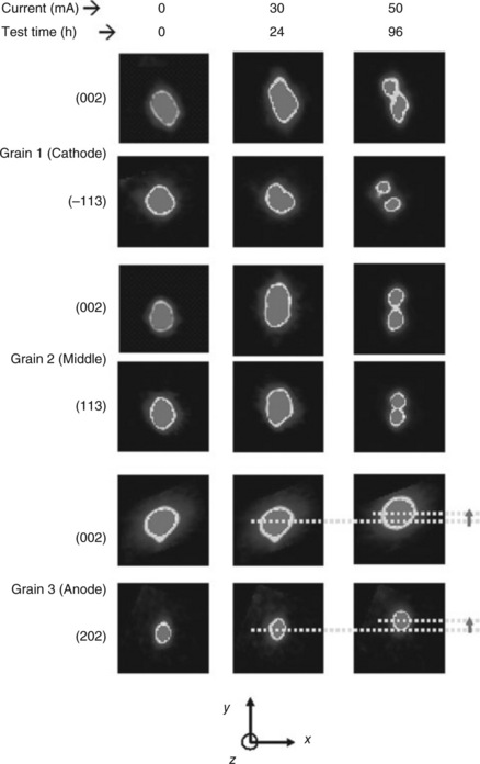
6.11 Evolution of Laue diffraction spots (in q-space) of three grains (one at the cathode end, one in the middle, and one at the anode end of the line) during an in situ EM experiment (Budiman et al., 2004; 2006a; 2006b). For each reflection, the area of q-space is kept constant with the length of each side of 0.03 Ǻ−1. Following the evolution of each spot, the reference location is kept constant.
The diffraction spots have been converted to q-space (reciprocal space), with the x-axis along the length of the line, the y-axis across the line, and the z-axis normal to its surface. We find that, as the electromigration test progresses, in certain grains the spots broaden, whereas in some grains, they split into two different spots. This broadening and splitting of diffraction spots is observed not in any random direction but always along the y-axis in q-space, which is the width direction of Cu line.
Broadening of the peak is observed in a few grains that are large and span across the width of the line. Figure 6.12a–6.12c display exemplary results of such grains, Grain 2 (in the middle of the line). Here the results of digital intensity traces across the broadening direction of the Diffraction spots in the initial, mid- and end-state (after the end of the electromigration test) are shown.
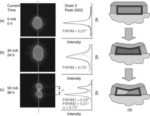
6.12 Quantitative measurement of the evolution of a Laue diffraction spot of Grain 2 during an in situ EM experiment (Budiman et al., 2004; 2006a; 2006b); Broadening is shown as the spot evolves from (a) to (b), and peak splitting, signifying the formation of low-angle grain boundaries, is evident in (c) as EM progresses. The evolution of Grain 2, in the cross-section of the line, is illustrated from undeformed, to plastic bending, to formation of sub-grain structures in (d).
Such broadening and splitting of the diffraction spots were observed in all three different wide test structure samples examined in our experiments. In each of them, a few grains (between 5 and 9) among a total of usually around 100 to 150 grains, were found to show this behavior after electromigration under similar test time, current and temperature.
The broadening of the diffraction spots represents crystal bending of the Cu grains in the line, whereas the split diffraction spots indicate the formation of low-angle boundary subgrain structures. From Fig. 6.12a–6.12c, it is thus evident that Grain 2 has evolved from initially, an undeformed crystal, to a plastically-bent crystal, and then lastly, to polygonized subgrain structures, such as illustrated in Fig. 6.12d. Each of the features here illustrates the corresponding Laue diffraction observations on the left side. From the amount of broadening we can calculate the bending of the Cu crystal, and from the amount of splitting, the angle of misorientation.
We can then use the broadening and the spot splitting observed to obtain information about the dislocation structure in the grain induced by electromigration. For instance, from the streak length of Fig. 6.12b as measured in the CCD camera and the sample to detector distance we obtain the curvature angle of the grain of 0.75°. Because the mapping of the out-of-plane orientation of the crystal along the Cu line indicates a near bamboo structure, the grain width is about the same as the width of the line (1.6 μm), from which we get the radius of curvature of the grain, R = 126 μm. The GND density to account for the curvature observed can be calculated from the Cahn–Nye relationship (Cahn, 1949; Nye, 1953), ρ = 1/Rb, where b is the Burgers vector. The GND density is then ρ = 3 × 109 cm−2. The total number of dislocations introduced is only 49.
To obtain quantitative information on polygonization walls (small angle grain boundaries) from the spot split in Fig. 6.12c we observe that the Laue spot splitting, Δθ = 0.73°. From this misorientation and Burgers’ model of a small angle grain boundary Δθ = b/L, where L = dislocation spacing, we find L = 212 Ǻ which amounts to 45 dislocations in the boundary.
Similar basic observations were made by Valek et al. (2002; 2003) in a related prior study in Al(Cu) interconnect lines in which a very early stage of plastic deformation and microstructural evolution during an electromigration test was also detected (shown in Fig. 6.13) long before any macroscopic damage became visible, by using the same technique (Budiman, 2008; Tamura et al., 2003; Valek et al., 2003). In addition, it was observed that, during in situ electromigration, a gradient of plastic deformation evolves along the line, resulting in bending and in polygonization of the largest grains between the cathode and the anode end. Smaller grains do not readily deform but do rotate as electromigration proceeds. Plastic deformation is initiated at the cathode end and gradually progresses toward the anode end until a steady state is reached. Further quantitative analyses of these Al(Cu) results were later conducted by Kai et al. (2008a; 2008b) and showed a consistent trend of plasticity in Al(Cu) as in Cu interconnect lines (Budiman et al, 2004; 2006a; 2006b).
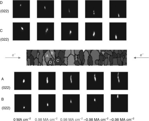
6.13 Similar observation of the EM-induced plastic deformation in Al(Cu) interconnects (Valek et al., 2002; 2003); The evolution of Laue diffraction spots from grains A, B, C and D (locations in the line are as shown in the grain mapping) from initial state to after some electromigration with reversed current directions. (courtesy of Valek, 2003)
Linewidth effects
We now describe in situ electromigration studies on another damascene Cu test structure with a different linewidth (0.6 μm). The higher test temperature of this group of experiments was designed to give more pronounced streaking of the Laue peaks as the grains undergo electromigration. A previous similar electromigration study has shown an extensive broadening of peaks in the Al(Cu) system (Valek et al., 2002; 2003). By increasing the test temperature of this group of experiments, we aim to have a similar homologous temperature (T/TM) to that of the previous study on Al(Cu), which was ~ 0.51. The homologous test temperature (T/TM) for the present study of narrow Cu lines was ~ 0.48, which is higher than the homologous temperature for the wide line experiments discussed above (~ 0.4).
However, our observation of the peaks of the grains in the narrow Cu line (width = 0.6 μm) did not show any broadening of the peaks during electromigration. This is true despite the higher temperature used in this group of experiments. Instead, grain rotations, similar to that of Grain 3 in Fig. 6.11, are observed throughout the length of the line. The rotation of grains manifests itself as a shifting in the position of the Laue spot; from the direction and magnitude of the shift, we can calculate the axis and amount of the crystal rotation.
The narrow Cu line thus appears to behave less plastically in response to similar electromigration current density stressing than the wide (1.6 μm) line. Narrower Cu lines thus seem to have higher electromigration resistance (than the wider Cu line). The resistance to plastic flow and the reasons why only grain rotation occurs in the narrow Cu line are not well understood at present. However, a higher resistance to plastic deformation in smaller structures, especially for Cu line structures, has also been reported by Spolenak et al. (2000; 2002).
In these studies (Spolenak et al., 2000; 2002), thermal cycling of the wide Cu damascene line (5 μm) was shown to exhibit plastic deformation with yield stresses in the range 50–100 MPa in compression (Fig. 6.14). In contrast, the narrower line (0.8 μm) in that study indicated no such yield behavior and deformed only elastically over the entire temperature cycling range. These observations are consistent with our electromigration results. Streaking of X-ray Laue spots indicating plastic bending of grains is observed for the wider 1.6 μm line, but is absent for the narrower line (0.6 μm).
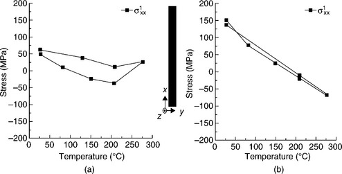
6.14 Deviatoric stress (σxx′) versus temperature graphs suggest plastic deformation in: (a) the wide (5 μm) Cu line, but not in: (b) the narrow (0.8 μm) geometry, consistent with the EM plasticity observation in Cu lines in the present study. (courtesy of Spolenak et al., 2002)
Effects of in-plane orientations
The consistent direction in which the electromigration-induced plasticity has been observed both in Al (Valek et al., 2002; 2003) as well as Cu interconnect lines (Budiman et al., 2004; 2006a; 2006b) was discussed earlier. Here, we further investigate the specific direction of the plastic deformation in term of electromigration current direction. We use the Laue peak streaking simulation to study the possible mechanisms of plasticity. By matching the simulation with the actual streaking pattern, we can make some conjectures as to which particular slip system, among the 12 possible slip systems known for FCC metals, might be responsible for the streaking pattern.
Coming back to the wide lines, Fig. 6.15 shows the movement of Laue spots of Grain 2 during the electromigration test, and a comparison with simulation result. Working within the Cahn–Nye crystal bending model (Cahn, 1949; Nye, 1953), and knowing the initial and end states of each of the diffraction spots, we can simulate the dislocation processes in the crystal necessary to cause the transformation of diffraction spots from their initial state to their final streaked/split/shifted state. We discovered that indeed the movement of the diffraction spots in Fig. 6.15a can be simulated by certain dislocation slip processes belonging to a slip system known to operate in FCC crystals (Fig. 6.15b). Figure 6.16a then describes the particular slip plane, slip direction and line direction in Grain 2 with respect to the interconnect line co-ordinates that are involved in the respective movement of diffraction spots.
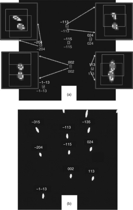
6.15 (a) Laue reflection spots at the initial stage (lower square) and after they split into the second set of reflection spots (upper square); (b) simulation of the same initial set of reflection spots streaked based on a particular slip system showing a match with experiment (Budiman et al., 2004; 2006a; 2006b).
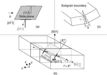
6.16 (a) The active slip system for which the simulation predicts the movement of reflection spots correctly in Fig. 6.15a and 6.15b; (b) Modeling of slip deformation in Grain 2; (c) subgrain boundary formation through polygonization (Budiman et al., 2004; 2006a; 2006b).
Grain 2 is a large grain spanning across the cross-section of the line, and thus can be modeled as shown in Fig. 6.16b. The simulation shows one possible scenario of evolution of the grain as electromigration progresses. Point defect transport on the interfaces of the Cu line initiates the production of dislocations within the crystal of Grain 2 and activates their movement. Dislocations glide on a {111} plane that is tilted 41° from the surface of the sample. As dislocations accumulate on the glide planes, they become unstable with respect to climb and begin to coalesce into tilt dislocation walls as illustrated in Fig. 6.16c. This series of events would manifest itself in the form of split Laue peaks following a certain direction as experimentally observed during electromigration to Grain 2 as shown in Fig. 6.15a.
We also observe that the < 112 > type direction for the tilt axis of the crystal is very close (within a few degrees) to the direction of the electron flow, or in other words, to the direction along the length of the line. The example in Fig. 6.16b shows a 6° deviation between the axis of tilt, which is a < 112 >, and the direction of electron flow. More specifically, upon further inspection, this particular < 112 > was also found to be the closest < 112 > in Grain 2 to the direction of electron flow.
Further, more complete, studies confirmed that this observation holds true for all the Cu grains in the current experiment exhibiting plastic bending and/or polygonization (formation of subgrain structures). This is shown in Fig. 6.17a. Nine large Cu grains with the observed plastic bending/polygonization are represented by the nine bullets within 10° of the closest < 112 > direction of their respective crystal to the direction of the electron flow. The bullets represent the direction of the in-plane crystallographic orientation of each of the respective grains in the direction of the electron flow in the line. To put it simply, all grains with a < 112 > direction pointing in the direction of the length of the line were observed with plastic bending/polygonization. More specifically, it has also been consistently observed that the particular < 112 > direction then becomes the tilt axis of the plastic deformation in the respective grain. This suggests a correlation of the proximity of certain < 112 > line directions to the direction of electron flow with the occurrence of plastic behavior.
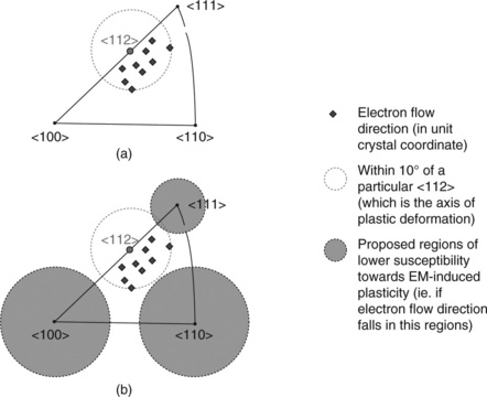
6.17 Proximity between a particular < 112 > direction (which is also the axis of plastic deformation) with the direction of the electron flow in the crystal is suggested to be correlated with the occurrence of EM-induced plastic deformation: (a) nine large Cu grains (Budiman et al., 2004; 2006a; 2006b) with the observed plastic bending/polygonization are represented by the nine bullets within 10° of a particular < 112 > direction; (b) the shaded regions represent preferred in-plane textures proposed to give higher resistance towards EM-induced plasticity.
We now recap our main observations up to this point. Almost immediately upon the application of high-density current flow, Cu grains behave plastically (crystal bending, polygonization, or simply rotation). We confirm that when large single grains spanning across the cross-section of the Cu lines are exhibiting crystal bending (and/or crystal polygonization), the rotation axis of this plastic deformation, which is always one of the < 112 > of the 12 possible slip systems in FCC crystals, was found to be very close (within 10°) to the direction of the electron flow, as illustrated in Fig. 6.17a. This particular < 112 > is also always the closest < 112 > to the direction of electron flow. This finding thus suggests that the proximity of a < 112 > direction in the grain to the direction of the length of the line is correlated to the occurrence of plastic behavior in a given grain.
This particular finding might have an important practical implication. If all the grains exhibiting crystal bending/polygonization are those with a < 112 > direction that falls closely within the direction of the electron flow, then we could propose that if a grain is oriented such that none of its < 112 > direction falls within 10° of the electron flow direction, then this grain would be less susceptible to plastic deformation induced by electromigration. Such grains have their crystallographic orientations in the direction of the electron flow if the lines fall within the shaded regions as shown in Fig. 6.17b. Therefore, it could be proposed that these are the particular in-plane textures of Cu interconnect lines that might give the wires lower susceptibility towards electromigration-induced plastic deformation, or in other words, higher resistance to electromigration later damage.
6.3 Plasticity and materials degradation mechanisms in copper interconnects
Most interconnect metals are aggregates of crystalline grains. The crystalline lattice of each grain has a characteristic orientation, and a polycrystal is thus characterized by a distribution of orientations: its texture. Texture governs many of the physical, electrical and mechanical properties of polycrystalline materials. In metallic conductor lines in microelectronics integrated circuits, texture has been known to play important roles in the performance and reliability of the conductors, for instance in electromigration (Vanasupa et al., 1999).
Plastic deformation was observed in damascene Cu interconnect test structures during an in situ electromigration experiment and before the onset of visible microstructural damage (i.e. voiding) using a synchrotron technique of white-beam X-ray microdiffraction. In this section, the extent of this electromigration-induced plasticity is shown to be dependent on the texture of the Cu grains in the line (Budiman et al., 2007a; 2007b; 2009). Furthermore, this dependence on texture has fundamental implications in terms of materials degradation mechanisms in Cu interconnects. We propose that this effect manifests itself in the increased effective diffusivity in the Cu interconnects during electromigration which expedites the degradation mechanisms leading to the eventual catastrophic events of failures (Budiman et al., 2007a; 2007b; 2009).
6.3.1 Electromigration-induced microstructural changes in Cu interconnects: effects of texture
In this section, we discuss a different set of Cu lines fabricated by a different manufacturer. This set of Cu lines differs with the previous set in a few ways; chief among them is texture. Again using the synchrotron technique of white-beam X-ray microdiffraction, we follow the evolution of plasticity in Cu polycrystals during similar electromigration experiments as in the previous section. We find strong texture dependence and propose a model to explain such prominent observation. In this set of samples, the Cu lines were surrounded by two different sets of dielectric materials. This has enabled us to also study the effect of dielectric constraints.
Experimental
The interconnect test structure used here (shown in Fig. 6.18) is a variation of a back-end-of-line (BEoL) process for a 65 nm CMOS technology manufactured by AMD, Inc. (Budiman et al., 2007a; 2007b; 2009). In this technology, the dual-damascene Cu fill process includes a standard Ta-based barrier and Cu seed, electroplated Cu fill, post-plating anneal, chemical-mechanical polish and a dielectric cap layer. Two different inter-layer dielectrics (ILD) were integrated with copper: Cu/low-k ILD (low-k = chemical vapor deposition (CVD) carbon-doped oxide) and Cu/hybrid ILD (hybrid = Cu/low-k at the line level and Cu/fluorine-doped tetraethyl orthosilicate (FTEOS) at the via layer). Both ILD materials were studied in order to provide a comparison of the extent of plasticity. The metal two (M2) lines were studied after partial removal of the top dielectric to expose the capped Cu lines (Fig. 6.18a). In these electromigration tests, the current was forced from the wide, upper metal layer (M3) into narrow M2 (called a V2M2 test) or from a wide lower metal layer (M1) into a narrow M2 (referred to as a V1M2 test). Both structures are designed to force failure in M2 at its critical dimension.
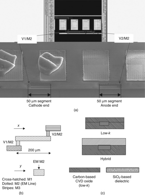
6.18 SEM images and schematic drawings of the Cu interconnect test structures in this experiment (Budiman et al., 2007a; 2007b; 2009): (a) SEM image of the test structure; (b) in situ EM experiment; (c) two sets of test structures of different dielectric schemes: low-k versus hybrid.
The first set of test structures consists of 200 μm-long lines, approximately 0.2 μm thick, and 0.5 μm wide. Owing to limited beam time, typical of synchrotron experiments, only segments of 50 μm length at both cathode and anode ends of the line were studied (Fig. 6.18a). The dielectric is carbon-based CVD oxide (‘low-k’ in Fig. 6.18c). The second set of interconnect test structures was prepared with dimensions similar to those of the first one, but with the hybrid ILD material (SiO2-based). The line length is 200 μm, the thickness is approximately 0.25 μm and the width is 0.7 μm. Similarly, only segments of 50 μm length at both cathode and anode ends of the line were studied.
The experiment was performed on the Beamline 7.3.3 (now Beamline 12.3.2) at the Advanced Light Source, Berkeley, CA. The electromigration test was conducted at 300 °C on a via-terminated test structure (Figure 6.18(b)). The current was ramped up to 2 mA (j = 2 MA cm−2) and then set at that value for the rest of the test (up to 36 h). The ambient temperature in the synchrotron end-station (hutch) where the tests were performed is 20 °C.
Electromigration-induced plasticity in copper interconnects
The in situ electromigration observations are described first. Figure 6.19 shows the typical evolution of the Laue diffraction spots during the in situ electromigration test. Figure 6.19 is early in the electromigration test (after 36 h of testing). The observed broadening of the Laue diffraction spots (streaking) represents plastic deformation of the Cu grains induced by electromigration (Budiman et al., 2004; 2006a; 2006b; Valek et al., 2002; 2003).
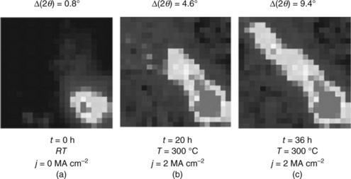
6.19 The typical evolution of Laue diffractions spots from Cu interconnect test structures during in situ electromigration experiments (Budiman et al., 2007a; 2007b; 2009).
As the electromigration test progresses, plasticity is observed in the Cu grains throughout the line, such as demonstrated in Fig. 6.20a. Plasticity here may manifest itself either in the form of diffraction spot broadening (streaking) or in the form of diffraction spot splitting (into two or even more different spots). The broadening of the diffraction spots represents crystal bending of the Cu grains in the line, whereas the split diffraction spots indicate the formation of low-angle boundaries or sub-grain structures (Budiman et al., 2004; 2006a; 2006b; Valek et al, 2002; 2003).
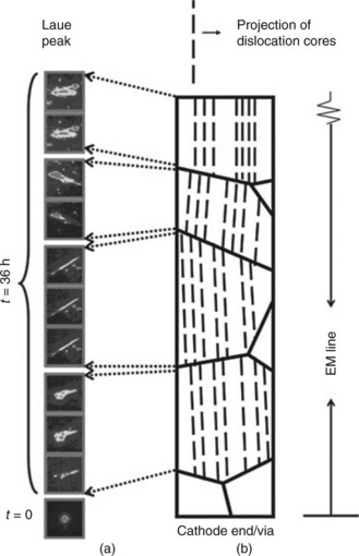
6.20 Laue diffraction images of the cathode end of the line after 36 h of testing (Budiman et al., 2007a; 2007b; 2009): (a) streaking and/or splitting of Cu Laue diffractions spots (each image represents a 0.5 μm step size) throughout a segment of the line observed; (b) Dislocations observed with cores aligned with the direction of the electron flow in the line (consistent with earlier observations in Budiman et al., 2004; 2006a; 2006b) across grains throughout the length of the segment of the line (the grain map is estimated based on the streaking observation; the total line length studied in each cathode or anode end is 50 μm, and the width is 0.5 μm).
Not only was plasticity observed, but also the direction of the plastic deformation is generally consistent across grains throughout the segments of the line under observation, as shown in Fig. 6.20a. This is consistent with our observation on the previous set of Cu lines (Budiman et al., 2004; 2006a; 2006b). Cu grains plastically deform in a direction transverse to the electron flow direction in the line. Such directionality can simply be accommodated by a distribution of same-sign edge dislocations with cores as illustrated in Fig. 6.20b, i.e. with the < 112 > line direction of the dislocations all lining up along the direction of electron flow in the line.
Exact grain orientation mapping of these Cu lines unfortunately could not be obtained in the present study. The X-ray spot size (0.5 μm × 0.5 μm) used in the Beamline 7.3.3 (now Beamline 12.3.2) was relatively large for the dimensions of these state-of-the-art interconnect lines. That makes diffraction spot indexing very difficult and thus mapping of grain orientations and other further quantitative analyses unreliable. The few Cu grains that we show in Fig. 6.20 were among the limited number of grains in the two Cu lines for which indexing of the diffraction spots happens to be sufficiently clear and unambiguous for this analysis. In general, the larger the Cu grains and the more bamboo-like they are, the more they diffract sharply and give numerous diffraction spots, thus giving higher confidence on the reliability of these results. That being said, it is fortunate that the evolution of Cu diffraction spots before and after some period of electromigration testing can still be compared qualitatively, as demonstrated in Fig. 6.19.
The extent of the electromigration-induced plasticity observed in the present samples is now determined. Figures 6.21a and 6.21b show still different additional diffraction spots observed during this experiment (after EM testing of 36 h, at 300 °C and 2 MA cm−2 current loading) from Cu lines with the low-k and the hybrid dielectrics, respectively. The diffraction spots have been converted to χ-θ angular space, with χ running along the direction of the length of the line, and θ across the direction of the width of the line. The χ-θ angles refer to the plane normals responsible for the Laue streaks.
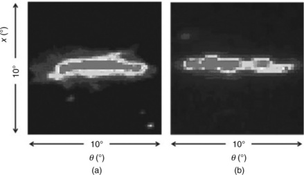
6.21 A χ-θ space/contour intensity plot of dielectric effects: the Laue peak streaking/splitting observed from Cu interconnect test structures (Budiman et al., 2007a; 2007b; 2009) with (a) low-k, and (b) hybrid dielectrics.
The observed broadening and spot splitting can be used to obtain information about the dislocation structure induced into the grain by electromigration. For instance, from the streak length of Fig. 6.21a, as measured in the digital camera image, and knowing the sample-to-detector distance, we determine the curvature angle of the grain to be 9.8°. Assuming a near bamboo structure, the grain width is the same as the width of the line (0.5 μm), from which we determine the radius of curvature of the grain, R = 2.34 μm. The GND density needed to account for the observed curvature can be calculated from the Cahn-Nye relationship (Cahn, 1949; Nye, 1953), ρ = 1/Rb, where b is the Burgers vector. The GND density is then ρ = 1.68 × 10¹⁵ m−2. The total number of dislocations in the area of the cross-section of the Cu line/grain is approximately 142.
To obtain quantitative information on polygonization walls (subgrain boundaries) from the spot split in Fig. 6.21b, we observe that the Laue spot splitting, Δθ = 9.1°. From this misorientation and Burgers’ model of a small-angle grain boundary, Δθ = b/L, where L = dislocation spacing, we find that L = 16 Ǻ which amounts to a total of 110 dislocations in the subgrain boundaries in the cross-section of the Cu line/grain. This translates to a GND density of ρ = 1.12 × 10¹⁵ m−2.
The extent of the plasticity as described here (ρ ~ 1015 m−2) is observed across all grains throughout the segments of both lines with different dielectric schemes. The significance of the difference in our analysis above, in terms of the extent of the plasticity, as well as, its manifestation (grain bending versus polygonization) between the two Cu lines with different dielectric schemes requires added confirmation. Nevertheless, they provide a general indication of the extent of plasticity in these Cu lines.
Effects of texture
Compared with the typical observation of the extent of the electromigration- induced plasticity in the previous set of Cu interconnect lines (Budiman et al., 2004; 2006a; 2006b), this set of samples exhibits at least a two-order of magnitude difference, in terms of GND density (Fig. 6.22). The samples studied in the previous section (referred to as ‘Samples A’) exhibited ρ ~ 1012–1013 m−2 (Budiman et al., 2004; 2006a; 2006b), and the samples in this section (referred to as ‘Samples B’) exhibited ρ ~ 1015 m−2 (Budiman et al., 2007a; 2007b; 2009). Samples A and B differ fairly significantly in dimensions, as well as the dielectric materials used, as shown in Fig. 6.22 (the dimensions are to scale).
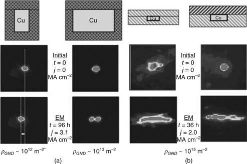
6.22 Schematics of the cross-sections, typical evolution of Cu Laue diffraction spots (from ‘Initial’ to ‘EM’ states), and the typical densities of GNDs implied by the extent of streaking/splitting of Laue peaks: (a) samples A (Cu lines reported in Budiman et al., 2004; 2006a; 2006b); and (b) samples B (Cu lines reported in (Budiman et al., 2007a; 2007b; 2009). (*taken as that of typical annealed metals).
Figure 6.22 shows the typical evolution of the Laue reflections from the Cu lines from the initial state (room temperature, j = 0, t = time = 0) to the electromigration state (after some electromigration, T = 300 °C, j ~ 2.0–3.1 MA cm−2, t ~ 36–96 h). Care was taken in order for the observed intensity contours in the χ-2θ co-ordinate in Fig. 6.22 to be similar (the windows all cover areas of squares of a range of 7° to 10° in angle space, and the threshold of the lower-bound intensity display was set to be similar). Thus, it is obvious from the relative apparent difference in the extent of streaking/splitting of the Laue diffraction spots that the level of plastic deformation that developed during the course of electromigration in Samples B is distinctly larger than that of Samples A.
As the two sets of samples (Samples A and B) under investigation are provided by different integrated circuit manufacturers, it is not possible to completely quantify the process differences (dielectric type, materials processing and thermal history) in their technologies in this section. It is known that the two sets of samples differ in terms of dimension and dielectric materials used; however, it is assumed that the main difference, as far as electromigration-induced plasticity is concerned, is the crystallographic texture of the Cu lines. From the texture analysis conducted in our previous study (Budiman et al., 2004), we know that Samples A have a rather weak (111) texture. As mentioned earlier, the exact grain mapping for the present study (Samples B) could not be obtained; however, Samples B came from the same manufacturer of the inlaid Cu lines studied by Besser et al. (2001). It is therefore reasonable to assert that Samples B would have the typical strong (111) texture as observed by Besser et al. (2001).
Although other process differences between these two sets of samples, including dimensions and dielectric materials, are acknowledged, we believe that these differences cannot satisfactorily explain the differences in the extent of plastic deformation. For example, the Cu in Samples A is surrounded completely by dielectric material, which is a fluorinated SiO2-based dielectric and, thus, generally believed to constrain the Cu lines better, and this should result in less plastic deformation. This is consistent with our observation of Samples A compared with Samples B, but the different dielectric schemes in Samples B, do not appear to affect the level of plasticity in the Cu lines. Another example involves the size effect. Wider lines seem to exhibit more plastic deformation in our previous study (Budiman et al., 2004; 2006a; 2006b), such as also shown in the previous section. However, Samples B are much narrower, and also much smaller in all cross-sectional dimensions, than Samples A, but Samples B exhibits two orders of magnitude more electromigration-induced plasticity.
Figure 6.23 is a summary of the known information about the Cu lines in Samples A compared with Samples B. First, Samples A shows a weak (111) texture, and we found the extent of electromigration-induced plasticity of the order of ρ ~ 1012–1013 m−2. Subsequently, Samples B was found with ρ ~ 1015 m−2 after similar electromigration conditions, a significantly larger amount of electromigration-induced plasticity. Besser et al. (2001) suggested that Samples B have the typical strong (111) texture. This observation of significantly larger electromigration-induced plasticity in Samples B than in Samples A, is consistent with our earlier observation, as described in the previous section, that the occurrence of plastic deformation in a given grain can be strongly correlated with the availability of a < 112 > direction of the crystal in the proximity of the direction of the electron flow in the line (within an angle of 10°). In < 111 > out-of-plane oriented grains in a damascene interconnect scheme, the crystal plane facing the sidewall tends to be a {110} plane, so as to minimize the interfacial energy (Paik et al., 2004; Besser et al., 2001; Sanchez and Besser, 1998). Therefore, it is deterministic rather than probabilistic that the (111) grains have a < 112 > direction nearly parallel to the direction of electron flow or the direction of the length of the line. This is illustrated in Fig. 6.23b.
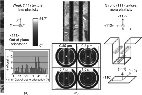
6.23 Comparison the texture correlation of: (a) samples A, Cu lines reported in Budiman et al. (2004; 2006a; 2006b), which have a weak (111) texture, and ‘less plasticity,’ and (b) samples B, Cu lines reported in Budiman et al. (2007a; 2007b; 2009), which have strong (111) texture, and ‘more plasticity.’ The schematic on the right illustrates that the strong preferred in-plane orientation of (111) grains leads to a preferred < 110 > to the sidewalls and < 112 > along the direction of length of the lines. (courtesy of Besser et al., 2001)
In Samples B, most grains are < 111 > in out-of-plane orientation (such as shown in the focused ion beam mapping in Fig. 6.23b), and thus prefer energetically to have the < 110 > directions normal to the sidewalls, thus causing a < 112 > direction to be very close to the direction of the electron flow. When this condition is met, our proposed correlation discussed in the previous section (Budiman et al., 2004; 2006a; 2006b) suggests that plasticity occurs in these Cu grains upon electromigration, and not only did it occur in this study, the extent of the plasticity here was rather extreme. Samples A, in the meantime, have only a few grains that are < 111 > in out-of-plane orientation, which leads to the occurrence of plasticity only in these few grains in the Cu lines after electromigration. In most other grains (i.e. non < 111>-oriented grains), a < 112 > direction of the Cu crystal is not likely to be the direction of the electron flow of the lines. Thus, plasticity was not observed in many grains in the Cu lines of Samples A.
6.3.2 Plasticity-amplified diffusion in electromigration
The observed plasticity described above (Fig. 6.20) leads to a concentration of same-sign edge dislocations with cores running along the direction of electron flow, as illustrated three-dimensionally in Fig. 6.24. When this configuration of same-sign edge dislocations extends through grains along the full length of the interconnect lines, the dislocation cores can serve as additional paths for diffusion of atoms from one end of the interconnect line to the other. Dislocation cores are, in general, already recognized as fast diffusion paths (Baker et al., 2000), but in this configuration especially, their contribution to the overall migration of atoms from the cathode to the anode end of the line is even more pronounced. Furthermore, when the concentration of these dislocations becomes high enough, their contribution to the overall effective diffusivity (Deff) can no longer be neglected.
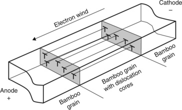
6.24 Schematic of a grain containing same-sign edge dislocations with cores running along the direction of the electron flow in the interconnect line.
In this context, the effective diffusivity can be written as:
where acore is the cross-sectional area of dislocation cores, Dcoreeff is the effective core diffusivity, ρ is the dislocation density, and δ, h and Dint are the effective interface diffusion thickness, the height of the line and the diffusivity of the interface, respectively. It is necessary here to use Dcoreeff, the effective core diffusivity (instead of simply Dcore, the core diffusivity), because for the dislocation cores to have an effect on mass flow along the full length of the line, a continuous diffusion path (across grains) must be available for atoms to transport from the cathode end to the anode end of the lines. Considering the mostly bamboo grain structure that our interconnect lines have (as shown in Fig. 6.20), this requires consideration of grain boundary diffusion, as atoms eventually hit the grain boundaries and have to travel some distance in the grain boundary before finding another set of dislocation cores (belonging to the neighboring grain) to continue their travel to the other end of the line. This is illustrated schematically in Fig. 6.25. Thus, the effective core diffusivity, Dcoreeff, here is defined as the effective diffusivity along the dislocation cores when the effect of the grain boundary diffusion is taken into account.
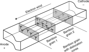
6.25 Illustration of bamboo grains with dislocation cores running along the direction of the electron flow in the line under electromigration bias. Dislocation cores from one grain end at the grain boundaries. Atoms traveling across multiple grains must diffuse along grain boundary regions, before finding another set of dislocation cores in the next grain.
It is obvious that only when the effect of the grain boundary diffusion is negligible (or in other words, the grain boundary diffusion is a fast enough process), can dislocation cores provide a competitive alternative diffusion path and influence the overall effective diffusivity Deff as suggested in equation 6.2. In order to study quantitatively the impact of this grain boundary diffusion on the overall dislocation core diffusion (Dcoreeff), we derive the kinetics for such a model and arrive at the expression below for Dcoreeff (the full derivation is provided in Budiman et al., 2009),
where δgb and Dgb are the effective width and diffusivity of the grain boundary, respectively, L is the overall length of the diffusion path, rcore is the radius of the dislocation core, and R is the mean distance in the grain boundary to the next dislocation core.
The influence of grain boundary diffusion on the overall/effective dislocation core diffusivity Dcoreeff, thus depends on the relative magnitude of the two terms in the denominator in the equation [6.3]. If:
then, as evident from equation [6.3], Dcoreeff degenerates into simply Dcore or, in other words, there is very little influence of the grain boundary diffusion in the overall scheme in Fig. 6.25. If the reverse is true, Dcoreeff is much smaller than Dcore, and the grain boundary slows down the overall diffusion significantly.
Referring now to the textbook values for grain boundary and core diffusion compiled in Table 6.1 (Cai et al., 1999; Dickenscheid et al., 1991; Frost and Ashby, 1982; Gan et al., 2006), and shown in Table 6.2, it is evident that the 2δgbDgbL term in equation [6.3], as well as in equation [6.4], is at least four orders of magnitude larger than the rcore2Dcore ln(R/rcore) term. This leads to the degeneration of Dcoreeff into simply Dcore in equation [6.3], reducing to equation [6.5]:
Table 6.1
Values used to determine the influence of grain boundary diffusion on the overall transport kinetics in the Cu line under EM. The diffusivities (Dgb, Dcore) are described in the usual way by D = Do exp(− EA/kT) where EA is the activation energy, Do is the pre-exponential constant, and k is the Boltzmann’s constant. The subscripts gb refers to grain boundary diffusion
| Variable | Value | Reference/remarks |
| T | 300 °C = 573 K | Following Ttest in 6.3.2 ‘Experimental’ |
| EA,gb | 1.08 eV | Frost and Ashby, 1982; Gan et al., 2006; Cai et al., 1999; Dickenscheid et al., 1991 |
| δgbDgb | 1.6 × 10⁻²⁴ m3 s−1 | Calculated (Frost and Ashby, 1982) |
| L | 1 μm | Estimated (Budiman et al., 2009) |
| rcore | 0.25 Ǻ | Frost and Ashby, 1982 |
| EA,core | 1.21 eV | Frost and Ashby, 1982 |
| rcore2Dcore | 7.3 × 10−36 m4 s−1 | Calculated (Frost and Ashby, 1982) |
| ρGND | 1015 m−2 | As observed in Budiman et al., 2009 |
| R | 22 nm | R = 1/2ρcore |
Table 6.2
Values of the two parameters/terms in equation [6.4] (or denominator of equation [6.3]) calculated from values listed in Table 6.1
| Parameter/term | Value |
| 2δgbDgbL | 3.2 × 10⁻³⁰ m4 s−1 |
| r2coreDcore ln(R/rcore) | 5.0 × 10⁻³⁵ m4 s−1 |
The practical implication of equation [6.5] is that a practically continuous pipe (dislocation core) diffusion path across multiple grains between the cathode end and the anode end of the line is indeed available for atomic transport in the Cu test structures under accelerated electromigration testing.
An ‘extreme’ assumption would be to take the activation energy for grain boundary diffusion EA,gb to be the EA for lattice diffusion, which is 2.04 eV (Frost and Ashby, 1982). This is a much higher activation energy than that of grain boundary diffusion. In this case, we show that the combined diffusivity would be dominated by such slow diffusion in the hypothetical ‘grain boundary.’ The effective transport through dislocation cores in this case would be slowed down by nearly four orders of magnitude owing to the effect of the hypothetical grain boundary. This is shown in Fig. 6.26, which compares calculated diffusivities as a function of temperature for three different schemes of diffusion (Dcore, Dcoreeff ‘as it is,’ and Dcoreeff ‘extreme,’ as defined above). The Dcoreeff ‘extreme’ line is close to four orders magnitude lower than Dcoreeff line (with crosses), which is practically on top of each other with the Dcore line (with buttons) as suggested by equation [6.5].
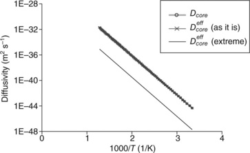
6.26 Comparison of diffusivities as a function of temperature between Dcore (only dislocation core diffusion, no grain boundary), Dcoreeff (considering the effect of grain boundary; as it is – as shown in Table 6.2), and an extreme Dcoreeff (considering the effect of grain boundary diffusion as if it is lattice diffusion). Diffusivities were calculated using values summarized in Table 6.1.
It is therefore reasonable to propose that a fully continuous network of dislocation cores running along the direction of the length of the line, slowed only by less than 0.01% by grain boundary diffusion, exists in the Cu interconnect lines studied during electromigration under accelerated test conditions in this study. This makes it a viable alternative for global transport of atoms in Cu interconnects under electromigration bias.
The existence of a viable path of dislocation core diffusion alone, however, is not sufficient to influence the overall kinetics in equation [6.2], that is, if the dislocation density (ρ or ρGND) is not high enough. We discuss this situation below and show the importance of the experimental results described in this section in understanding the overall kinetics in Cu interconnect lines under electromigration.
Diffusion along dislocation cores (‘pipe diffusion’) has been commonly included in models of diffusion-controlled deformation in bulk materials (Frost and Ashby, 1982). Suo (1994) considered the motion and multiplication of dislocations under the influence of an electric current in a conductor line, and suggested that electromigration-driven dislocation multiplication could itself lead to dislocation densities high enough to affect electromigration degradation processes. Oates (1996), however, did not see any diffusivity effects that could be attributed to dislocations in his experimental study. Baker et al. (2000) through their experimental study of nanoindented Al lines (width = 1 μm, mean grain size = 1.1 μm) showed that the effect of a dislocation density of 1016 m−2 is similar to diffusion through a grain boundary. These studies all essentially suggest that if the dislocation density is sufficiently high, it may affect the overall electromigration degradation processes in metallic interconnects, and thus could have fundamental implications.
Materials degradation mechanisms
We have, earlier in the manuscript, established that dislocations with cores running along the electron flow direction and densities in the order of 1015 m−2 are present in the Cu lines undergoing electromigration (accelerated test conditions) for 36 h. Figure 6.27 is a comparison of calculated diffusivities as a function of temperature between the interface diffusion path and those of dislocation cores of various densities in Cu interconnect lines (1012 m−2, 1015 m−2, and 1017 m−2) when each diffusion mechanism is assumed to act alone. The diffusivities are calculated based on diffusion coefficient values in the literature (Frost and Ashby, 1982; Gan et al., 2006) for Cu interconnect lines (Table 6.3), and for the interconnect dimensions as described earlier in this section.
Table 6.3
Values used to determine diffusions in Cu interconnects as a function of temperature (Fig. 6.27). Do is the pre-exponential constant and EA is the activation energy. The subscripts int and core refer to interface and core diffusions, respectively. The δ is the effective interface diffusion thickness, h is the thickness of the Cu lines, and acore is the area of a dislocation core
| Variable | Value | Reference/remarks |
| δDo,int | 3.4 × 10⁻¹⁹ m3 s−1 | Based on SiN/Cu (Gan et al., 2006) |
| H | 0.2 μm | Budiman et al., 2009 |
| EA,int | 0.91 eV | Based on SiN/Cu (Gan et al., 2006) |
| acoreDo,core | 1.0 × 10⁻²⁴ m4 s−1 | For copper (Frost and Ashby, 1982) |
| EA,core | 1.21 eV | For copper (Frost and Ashby, 1982) |
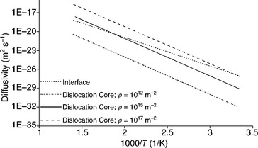
6.27 Calculated diffusivities as a function of temperature between the interface diffusion path and those of dislocation cores of various densities in Cu interconnect lines (1012 m−2, 1015 m−2, 1017 m−2). Each diffusion mechanism is assumed to act alone (Budiman et al., 2009).
The dislocation density observed in the present study (ρGND = ρcore = 1015 m−2) is illustrated as the solid line in Fig. 6.27, illustrating that dislocation core diffusion is on the same order of magnitude as that of interface diffusion (the dotted line) at the test conditions (T = 300 °C or 1000/T = 1.75/K). Thus, a core dislocation density of 1015 m−2 is the dislocation density threshold necessary for dislocation core diffusion to be on a par with interface diffusion. In other words, at this dislocation density the contribution of dislocation cores to the overall/effective diffusivity in the Cu line during accelerated electromigration is expected to be at least the same order of magnitude as interface diffusion and thus cannot be neglected.
It is to be noted, however, that at temperatures at or below 100 °C, the required dislocation density for cores to have a significant contribution to the diffusion would be on the order of 1017 m−2 (the dashed line in Fig. 6.27). These lower temperatures correlate with the typical use or operational conditions of the interconnects. The typical initial (as fabricated) dislocation density in Cu/metallic lines was taken to be 1012 m−2 (following Baker et al., 2000), and the corresponding diffusivity is shown by the dashed-dotted line in Fig. 6.27.
It is therefore reasonable to propose that the contribution from the dislocation core diffusion (the second term in equation [6.2]) can no longer be neglected in the Cu lines now that we have evidence of the existence of such high density of dislocation cores in the real Cu interconnect structure. It is certainly true in the Cu lines investigated in the present study especially during electromigration at accelerated test conditions. The contribution from dislocation cores would enhance the electromigration diffusion, or in other words, the total electromigration flux (JEM), since the total or overall diffusion includes the existing, usually-dominant interface diffusion, plus the observed dislocation core or ‘pipe’ diffusion. The increase in this core diffusion to the point of significance in the overall electromigration diffusion is related to the kind and the extent of plasticity induced by the electromigration process itself (i.e. through the increase in the core dislocation density from the pre-electromigration density ρcore = 1012 m−2 to the observed density ρcore = 1015 m−2).
The result of this study gave a key piece of experimental evidence that opens up the possibility that such a high dislocation density may generally be present in the Cu test structures undergoing electromigration. The circumstances and the important implications of this special configuration of dislocation cores for the electromigration degradation processes warrant discussion, as do the electromigration reliability assessment methodologies. With ρGND ~ 1015 m−2 observed in this study, and Dcoreeff that is not much reduced by grain boundary diffusion (as derived above and in Budiman et al., 2009), the second term in equation [6.2] (i.e. the contribution of the dislocation core diffusion) can indeed no longer be neglected. This means it will have important implications to the fundamental understanding of the electromigration degradation processes, as well as to the electromigration reliability assessment methodologies.
6.4 Implications for the reliability of advanced copper interconnect schemes
Electromigration is a major reliability concern in the advanced microelectronics industry. This is because of the aggressive scaling of interconnect dimensions and the recent introduction of new materials and processing schemes leading to even more challenges in guaranteeing interconnect robustness against electromigration failure. Understanding the fundamental relationship between electromigration in interconnect lines and parameters of materials and processing that make up the interconnect structures, is thus very important.
In addition, it is also useful, especially for industry, to accurately assess the lifetime of the device under electromigration conditions. This involves taking data under accelerated conditions (such as high temperatures and current densities) and scaling it back to the device operational conditions. This electromigration lifetime extrapolation is commonly based on the well-established Black’s Law (Black, 1967). This methodology for extrapolations determines whether a technology is sufficiently reliable against electromigration failure for a given specification, or whether further optimization in process and/or design is needed.
Black’s Law (Black, 1967) expresses the median time to failure (MTF), or the 50th percentile fail time of a failure population, as:
where A is an empirically-determined constant, j is the current density, n is the current density exponent, EA is the activation energy to electromigration failure, k is the Boltzmann’s constant and T is the absolute temperature.
The figure of merit for electromigration reliability is the use current density (current density at device operational conditions), which is commonly denoted as juse or jmax, and represents the maximum current density the interconnect system can maintain while still guaranteeing a certain failure rate over a certain amount of operation time at use conditions. Therefore the current density exponent n is crucial, as the extrapolated failure time (i.e. device lifetime at use/operational conditions) is very sensitive to it.
Although Black’s equation, equation [6.6] is widely used, the value for the current density exponent and its implications to electromigration lifetime prediction are still much debated (Budiman et al., 2010; Hau-Riege, 2004; Hu et al., 1999; 2007; Kirchheim and Kaeber, 1991; Roy and Tan, 2008; Shatzkes and Lloyd, 1986). Under the common atomistic description of electrotransport (Verhoeven, 1963), the flux in the electromigration of a metallic line is proportional to the current density and the product of flux and time (i.e. MTF) and corresponds to the removal of a certain volume of matter per unit length (i.e. the cross-section area) of the interconnect line, which is a necessary condition for failure. Thus we have MTF ~ j−1 (i.e. n = 1). This description is usually associated with a void growth limited failure mode (Hau-Riege, 2004; Hau-Riege et al., 2002), as opposed to a void nucleation limited mode, which has also recently been supported by experimental observation (Zschech et al., 2004). These concepts appear to be applicable to the case of Cu interconnects (Hau-Riege et al., 2002).
However, it has been widely observed that the current density exponent n is usually found in real cases to be > 1 (Budiman et al, 2010; Hau-Riege, 2004; Hu et al., 1999; 2007; Kirchheim and Kaeber, 1991; Roy and Tan, 2008; Schafft et al., 1985; Shatzkes and Lloyd, 1986) as opposed to n = 1 for the prevailing model of void growth limited failures. This suggests that there is an extra dependency on j, under accelerated test conditions. This extra dependency has been attributed to the effect of Joule heating (Bobbio and Saracco, 1975; Kirchheim and Kaeber, 1991; Schafft et al., 1985; Sigsbee, 1973). Joule heating is the process by which the passage of an electric current through a conductor releases heat. It is caused by interactions between electrons that make up the body of the conductor. At higher j (accelerated/test conditions), more electrons are passing in the interconnect line, causing more heating, and thus a higher temperature (making it even higher than the accelerated/test temperature), leading to amplification of electromigration diffusion in the interconnect lines, and thus earlier failure events. This manifests in the Black’s Law as an extra dependency on j, or in other words, the deviation of n from unity (and/or from n = 2, for that matter).
6.4.1 Inflated current density exponent n
If ρ increases with j, then we find that Deff (the overall/effective diffusivity of the electromigration process) also increases with j. Consequently, there is an extra electromigration flux, and thus an extra reduction in the time to failure of the device with increasing j. This is an extra dependency on j, which manifests itself in the value of the current density exponent n in Black’s equation [6.6], being > 1.
Kirchheim and Kaeber (1991) first experimentally observed the MTF dependency on current density j in an Al conductor line, for a wide range of j, such as shown in Fig. 6.28 (the solid black dots with error bars were the original data points). It clearly shows that at low current densities, the MTF data is best fit by n = 1 (straight solid line), whereas at higher current densities, the MTF data is better fit by n > 1 (curved dotted line). Kirchheim and Kaeber (1991), however, suggested that these deviations occurring at higher current densities might be caused by Joule heating.
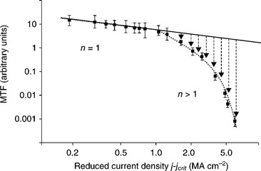
6.28 Kirchheim and Kaeber’s experimental MTF data as a function of reduced current density, j – jcrit (all the solid features); the dotted and dashed lines have been added as described in the text. (reproduced manually here to the highest accuracy possible from Kirchheim and Kaeber (1991); for clarity and improved image resolution), (courtesy of Kirchheim and Kaeber, 1991)
Similar experimental observation of the MTF dependency on current density j for a wide range of j, in the Cu interconnect lines has recently been reported by Budiman et al. (2010). Figure 6.29 shows the electromigration failure time as a function of current density in the electromigration tests performed on Cu interconnect samples very similar to the ones studied in the previous section (Budiman et al., 2007a; 2007b; 2009). Both samples were fabricated in the same wafer fabrication facility using the same 65 nm CMOS technology node. Thus, we can reasonably expect similar microstructural evolution during electromigration (as described in the previous section as well as in Budiman et al., 2009) also occurred with this set of samples (Budiman et al., 2010).
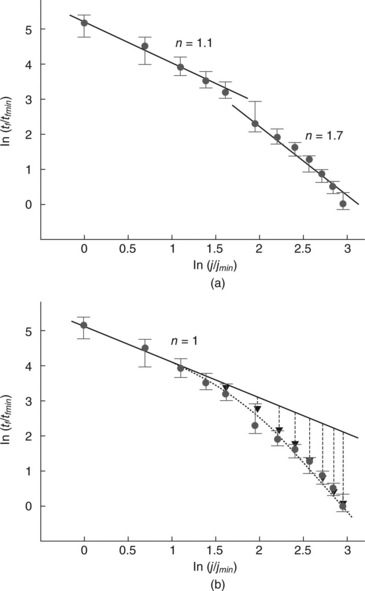
6.29 Electromigration (EM) test data/results from the Cu interconnect lines (Budiman et al., 2010) showing (a) n = 1.1 in the low j range, whereas n = 1.7 in the high j range, or, alternatively, (b) that n is principally 1 (the solid line) but MTF tends to be depressed in high j range (the dotted line) owing to extrinsic effects (the dashed line/arrow), as suggested by Kirchheim and Kaeber (1991). Note that the EM failure time data (the median as well as range; the solid circle and the error bar) as a function of j are identical between (a) and (b).
The median time to failure (MTF) in Fig. 6.29 is represented by the solid circle, whereas the error bar represents the range of the failure times coming from the 20 samples at each of the test conditions. All failure times are normalized with respect to the minimum MTF observed in the present study. No actual failure times are given here for proprietary reasons. The current densities are also normalized with respect to the minimum value in the present study, which is 0.5 MA cm−2. The data can be broadly divided into two groups; the low current densities (with ln j /jmin < 1.6, or j < 2.5 MA cm−2) and the high current densities with j > 2.5 MA cm−2. As we can see in Fig. 6.29a, the data in the low j range is best fit by a straight line with a slope of − 1.1, which indicates n = 1.1 in Black’s equation (Black, 1967) whereas in the high j range, n = 1.7. These results are consistent with the trend in Cu electromigration that has been reported recently by several researchers (Hu et al., 1999; 2007; Roy and Tan, 2008), most notably by Hu et al. (2007) who reported n = 1.1 and 1.8 for low and high current densities, respectively, under similar electromigration test conditions.
Alternatively, we may also suggest that n is principally 1 (especially true in the lower j range as indicated by the solid line in Fig. 6.29b), but that the MTF tends to be depressed in the high j range, which, in turn, causes the n value to deviate from the n = 1 line. Kirchheim and Kaeber (1991) attributed this extra depression of MTF in the high j range on a Joule heating effect. Earlier in situ studies (Budiman et al., 2004; 2006a; 2006b, 2007a; 2007b; 2009; Kai et al, 2008a; 2008b; Valek et al, 2002; 2003) observing microstructural changes and their evolution in Al as well as Cu interconnects during electromigration tests have also suggested EM-induced plasticity that can lead to new paths for electromigration transport which could also be responsible for this deviation (Budiman et al., 2009).
Plasticity, especially in the form described in this chapter as well as by Budiman et al. (2007a; 2007b; 2009) in Cu interconnects schemes could just as likely be the source of such deviations of MTF dependency on j at high current densities (Budiman et al., 2009; 2010). As j increases, plasticity also increases leading to increasingly higher electromigration fluxes (the dashed, arrowed lines in Fig. 6.28 as well as in Fig. 6.29) and, thus, increasingly lower MTF, and therefore eventually a current density exponent n > 1 has to be used to fit the failure time distribution.
However, if this deviation were caused by Joule heating alone then the effects would not be permanent; if the same sample were subsequently subjected to electromigration testing with low j, the degradation in failure times should not be retained. This hypothesis motivated us to study the second set of samples: the ‘pre-damaged’ samples (Budiman et al., 2010). The pre-damaged samples are the Cu interconnect samples that had been previously subjected to accelerated electromigration testing (at T = 350 °C and j = 3.5 MA cm−2 for a brief period of 50 h), i.e. the ‘pre-damaging’ phase. If Joule heating is wholly responsible for the deviation from n = 1, then the effects of this ‘pre-damaging’ phase would not be permanent and the failure times for this second set of samples should be about the same as for the nominal samples. On the other hand if the ‘pre-damaging’ phase causes a permanent change in the diffusional pathways, then the effects would be permanent and the degraded failure times would be retained for electromigration testing with low j (or in other words the failure times for the second set of samples should be significantly lower than those of the nominal samples). This is the main focus of the next subsection.
Joule heating effect versus electromigration-induced plasticity
A recent study comparing two sets of samples in which the main difference was the initial microstructures of Cu interconnects (Budiman et al., 2010) aims to provide insights into this question. The first set has been described above (Fig. 6.29) and is expected to have typical initial microstructures of annealed Cu grains. The second set is expected to have plastically deformed microstructures based on our earlier plasticity observations on similar Cu interconnect samples (Budiman et al., 2007a; 2007b; 2009). The experiment has been described in great detail by Budiman et al. (2010).
Electromigration test results for the two sets of samples: nominal versus ‘pre-damaged’ are compared in Fig. 6.30a. The electromigration test results of the nominal samples have been discussed above (Fig. 6.29). The median times to failure (MTFs) here are again represented by the solid features (circles for nominal samples and squares for the ‘pre-damaged’ ones), and the error bars represent the ranges of the failure times coming from the 20 samples from each group at each of the test conditions. All failure times are again normalized with respect to the minimum MTF observed in the present study. The current densities are also normalized with respect to the minimum value, which is 0.5 MA cm−2. It is clear from these data sets that there is a significant difference in time to failure between samples from the two different groups especially in the low j range (ln j/jmin < 1.95 or j < 3.5 MA cm−2).
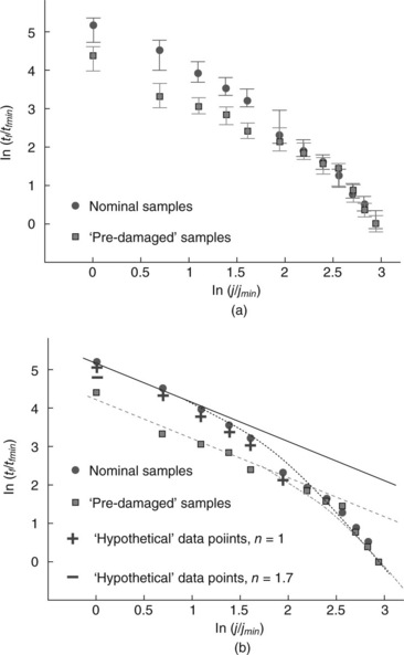
6.30 Electromigration (EM) test results (Budiman et al., 2010): (a) comparison between the nominal versus ‘pre-damaged’ samples, and (b) n is principally 1 in both cases (the solid line for the nominal samples, and the dashed line for the ‘pre-damaged’ samples) but MTF tends to be depressed in the high j range owing to extrinsic effects and thus deviating (the dotted line for the nominal samples, and the dashed-dotted line for the ‘pre-damaged’ samples) from the n = 1 trajectories; the ‘hypothetical’ data points (the ‘plus’ and ‘minus’ signs) indicate the shortened lifetime of the ‘pre-damaged’ samples if the ‘pre-damaging’ phase degrades the MTF more than its nominal 50 h owing to the very aggressive void growth.
In Fig. 6.30b, we consider just the MTFs of two sets of samples (the solid data points; without the error bars for clarity). The significant difference in the MTFs between the two sets of samples in the low j range suggests that Joule heating alone cannot be responsible for the deviation of MTF from the n = 1 line at the high j range such as shown in Fig. 6.29b. However, because the ‘pre-damaging’ phase was done at accelerated conditions of high temperature and high current density (at T = 350 °C and j = 3.5 MA cm−2) even though for a very brief period of time (50 h), it could perhaps cause very aggressive void growth such that the failure times for the second set of samples become somewhat lower than those of the nominal samples. In order to account for this equivalent lifetime used by the ‘pre-damaging’ phase, we now add the ‘hypothetical’ data points (i.e. the ‘plus’ and ‘minus’ signs) to indicate the shortened lifetime of the ‘pre-damaged’ samples if the ‘pre-damaging’ phase degrades the MTF more than its nominal 50 h owing to the very aggressive void growth.
The ‘equivalent’ lifetimes used by the ‘pre-damaging’ phase (the ‘plus’ and ‘minus’ signs) here were calculated using the proportionality assumption (i.e. MTF(j)n = constant; MTF′ = (j/j′)nMTF; for the ‘plus’ signs, as the ‘pre-damaging’ phase was actually done at j = 3.5 MA cm−2 for 50 h, the ‘equivalent’ lifetime used at j = 0.5 MA cm−2 is 350 h, that is 7 times, 3.5 MA cm−2 divided by 0.5 MA cm−2 with n = 1, the nominal 50 h). Even if we assume an extremely aggressive void growth during the ‘pre-damaging’ phase and thus introduce an n = 1.7 such as actually determined from the data shown in Fig. 6.29a for the conditions in the ‘pre-damaging’ phase to the above proportionality calculation, the hypothetically degraded MTF would then be shown as the ‘minus’ signs in Fig. 6.30b. Evidently, there remains a significant gap with the MTFs of the second set of samples.
These data sets thus strongly indicate that Joule heating cannot act alone here in these Cu interconnect samples. In the range of ln j/jmin < 1.95, the MTFs of the ‘pre-damaged’ samples (the square data points) are still significantly reduced from those of the nominal samples even after considering the shortened lifetime owing to the ‘pre-damaging’ phase (the ‘plus’ and ‘minus’ signs). Such a significant difference can be explained by electromigration-induced plasticity which introduces some permanent effects, perhaps in addition to the Joule heating effect. The significant difference here strongly suggests that the second set of samples have also suffered substantially higher electromigration fluxes than those of the first set of samples even though both were tested at the same low j, which further indicates there might be effects of a structural permanent difference between the two sets of samples. We believe that the high j ‘pre-damaging’ phase for 50 h had created dislocation configurations at such high densities that they had accordingly aggravated the electromigration fluxes in the second set of samples beyond the nominal 50 h or even beyond the hypothetically degraded lifetimes owing to the aggressive/extremely aggressive void growth scenarios during the ‘pre-damaging’ phase.
Even though Joule heating is widely cited as the source of the deviation from n = 1 at high j, recent studies (Chang et al., 2003; Hau-Riege, 2006; Labun and Jagjitkumar, 2008; Wang et al., 2004; Wu et al., 2001) both experimentally as well computationally have shown that its effects on the global transport of atoms along the metal interconnect lines are somewhat modest. In the absence of extreme local instabilities (such as hot spots or local meltdown owing to current crowding effects, for instance), the effect of Joule heating is predicted to be merely a rise of between 5 and 10% at high j compared with at low j in the global temperature of the interconnect lines (Chang et al., 2003; Gurrum et al., 2008; Hau-Riege, 2006; Labun and Jagjitkumar, 2008; Wang et al., 2004; Wu et al., 2001). This is insufficient to cause a large drop in MTF at high j that would be required to cause the n to deviate from n = 1 line significantly. This is especially true for the case of the Cu–SiO2 interconnect scheme, such as used in the present study, owing to the high thermal conductivity of SiO2 (Wu et al., 2001). For the Cu–SiO2 interconnect scheme, Wu et al. (2001) for instance using a combination of an analytical thermal model with a two-dimensional (2D) numerical simulation using the finite element method, has reported a less than 7% rise in global interconnect temperature at j = 4.5 MA cm−2 compared with at j = 0.5 MA cm−2 and, consequently, a factor of less than 2 in the MTF reduction owing to the temperature rise. The corresponding test conditions in the control data sets (i.e. the nominal samples) in the present study show at least a factor of 20 in the MTF reduction.
6.4.2 The danger of overestimating device lifetime
Finally, having recognized that any value of n larger than one obtained from accelerated test conditions (i.e. high j values) is the result of extrinsic effects, we reiterate the danger of overestimating device lifetime using the current methodology. If, for instance, we use the n = 1.7 as observed in the present study to extrapolate from the accelerated condition (high j) to the use condition (low j), that extrapolation would clearly lead to an overestimation of the device’s actual lifetime (approximated by the actual MTF data point at low current density). This is illustrated by the dashed–dotted line in Fig. 6.31.
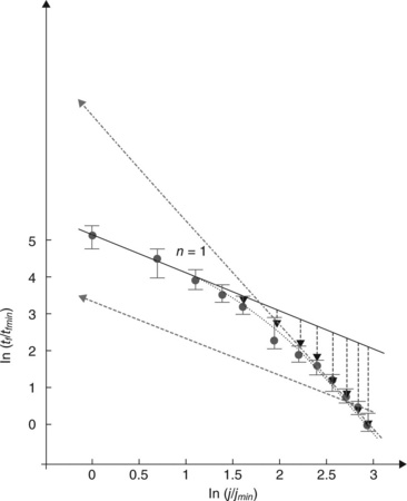
6.31 Illustration of the impact of the current exponent (n) on the extrapolated lifetime. The danger of overestimation of device lifetime by using n > 1 is shown (dotted-dashed line), as is the more conservative extrapolation using n = 1 (dashed line), which is closer to the actual device lifetime in use conditions. Data from Fig. 6.29 is again used here for illustrative purposes.
To improve the accuracy of the reliability assessment of devices under use conditions, we thus propose that the extrinsic effect has to be removed from the electromigration lifetime equation. This can be done simply by insisting on n = 1 in our lifetime assessment (illustrated by the dashed line in Fig. 6.31), which in most typical electromigration test conditions results in a more conservative prediction of device lifetime. This is true no matter whether Joule heating alone or, as we have proposed in the present study, electromigration-induced plasticity (in addition to Joule heating) is the root cause of deviation of MTF at high j in the electromigration of Cu interconnects.
6.5 Conclusions and future trends
In studying the evolution of the microstructure in the Cu interconnects during electromigration using the synchrotron-based X-ray microdiffraction technique, we have unraveled a new phenomenon which has not so far been taken into consideration and which might thus change our current understanding of the electromigration degradation mechanisms. This unraveling of these plastic behaviors of copper polycrystalline lines undergoing high current density flux was made possible by the white-beam nature of the X-ray source used in the μSXRD technique. The current understanding of the electromigration phenomenon so far has only included the elastic response of the metallic grains against the global atomic migration in the interconnects. Our results show that this might not be the whole story as plasticity comes into the picture. Furthermore, when the extent of this plasticity is sufficiently high, this particular configuration could lead to enough additional electromigration flux to start changing the kinetics of the electromigration lifetime prediction. This would certainly have important industrial as well as fundamental implications. As advanced interconnect schemes push further and further into the nanometer regimes of the materials near their microstructural inhomogeneities, plasticity will continue to play significant roles in determining the overall responses of the devices under operational loading.
6.6 References
Baker, S.P., Joo, Y.C., Knaub, M.P., Artz, E. Electromigration damage in mechanically deformed Al conductor lines: dislocations as fast diffusion paths. Acta Mater. 2000; 48:2199.
Besser, P.R., Zschech, E., Blum, W., Winter, D., Ortega, R., Rose, S., Herrick, M., Gall, M., Thrasher, S., Tiner, M., Baker, B., Braeckelmann, G., Zhao, L., Simpson, C., Capasso, C., Kawasaki, H., Weitzman, E. Microstructural characterization of inlaid copper interconnect lines. J Electron Mater. 2001; 30(4):320.
Black, J.R. Mass transport of aluminium by momentum exchange with conducting electrons. IEEE Proc 6th Ann Int Reliab Phys Symp. 1967; 148–159.
Bobbio, A., Saracco, O. Modified reliability expression for the electromigration time-to-failure. Microelectron Reliab. 1975; 14:431–433.
Bragg, W.L. The diffraction of short electromagnetic waves by a crystal. Proc Camb Philos Soc. 1913; 17:43–57.
Budiman, A.S. Probing plasticity at small scales: from electromigration in interconnects to dislocation hardening processes in crystals. Palo Alto: Stanford University; 2008.
Budiman, A.S., Besser, P.R., Hau-Riege, C.S., Marathe, A., Joo, Y.C., Tamura, N., Patel, J.R., Nix, W.D. Electromigration-induced plasticity: texture correlation and implications for reliability assessment. J Electron Mater. 2009; 38:379–391.
Budiman, A.S., Han, S.M., Greer, J.R., Tamura, N., Patel, J.R., Nix, W.D. A search for evidence of strain gradient hardening in Au submicron pillars under uniaxial compression using synchrotron X-ray microdiffraction. Acta Mater. 2008; 56:602–608.
Budiman, A.S., Hau-Riege, C.S., Baek, W.C., Lor, C., Huang, A., Kim, H.S., Neubauer, G., Pak, J., Besser, P.R., Nix, W.D. Electromigration-induced plastic deformation in Cu interconnects: effects on current density exponent, n, and implications for electromigration reliability assessment. J Electron Mater. 2010; 39:2483–2488.
Budiman, A.S., Hau-Riege, C.S., Besser, P.R., Marathe, A., Joo, Y.C., Tamura, N., Patel, J.R., Nix, W.D. Plasticity-amplified diffusivity: dislocation cores as fast diffusion paths in Cu interconnects. IEEE Proc 45th Ann Int Reliab Phys Symp. 2007; 122–127.
Budiman, A.S., Hau-Riege, C.S., Besser, P.R., Marathe, A., Joo, Y.C., Tamura, N., Patel, J.R., Nix, W.D. ‘Electromigration-induced plasticity and texture in Cu interconnects’, AIP Conference Proceedings, 9th. International Workshop on Stress-Induced Phenomena in Metallization. 2007; 945:56–65.
Budiman, A.S., Li, N., Baldwin, J.K., Xiong, J., Luo, H., Wei, Q., Tamura, N., Kunz, M., Chen, K., Misra, A., Growth and structural characterization of epitaxial Cu/Nb multilayers. Thin Solid Films 2011;, doi: 10.1016/j.tsf.2010.12.077.
Budiman, A.S., Tamura, N., Valek, B.C., Gadre, K., Maiz, J., Spolenak, R., Caldwell, W.A., Nix, W.D., Patel, J.R. Unexpected mode of plastic deformation in Cu damascene lines undergoing electromigration. Proc Mater Res Soc Symp. 2004; 812:345–350.
Budiman, A.S., Tamura, N., Valek, B.C., Gadre, K., Maiz, J., Spolenak, R., Nix, W.D., Patel, J.R. Crystal plasticity in Cu damascene interconnect lines undergoing electromigration as revealed by synchrotron X-ray microdiffraction. Appl Phys Lett. 2006; 88:233515.
Budiman, A.S., Tamura, N., Valek, B.C., Gadre, K., Maiz, J., Spolenak, R., Patel, J.R., Nix, W.D. Electromigration-induced plastic deformation in Cu damascene interconnect lines as revealed by synchrotron X-ray microdiffraction. Proc Mater Res Soc Symp. 2006; 914:295–304.
Cahn, R.W. Recrystallization of single crystals after plastic bending. J Inst Metals. 1949; 76:121–143.
Cai, B., Kong, Q.P., Lu, L., Lu, K. Interface controlled diffusional creep of nanocrystalline pure copper. Scr Mater. 1999; 41:755–759.
Chang, C.W., Gan, C.L., Thompson, C.V., Pey, K.L., Choi, W.K., Chua, M.H. Joule heating-assisted electromigration failure mechanisms for dual damascene Cu/SiO2 interconnects. Proc 10th IEEE Int Symp Phys Fail Anal Integr Circuits (IPFA). 2003; 69–74.
Chen, K.C., Liao, C.N., Wu, W.W., Chen, L.J. Direct observation of electromigration-induced surface atomic steps in Cu lines by in situ transmission electron microscopy. Appl Phys Lett. 2007; 90:203101.
Chung, J.S., Ice, G.E. Automated indexing for texture and strain measurement with broad-bandpass X-ray microbeams. J Appl Phys. 1999; 86:5249–5255.
D’Haen, J., Cosemans, P., Manca, J.V., Lekens, G., Martens, T., DeCeuninck, W., D’Olieslaeger, M., De Schepper, L., Maex, K. Dynamics of electromigration induced void/hillock growth and precipitation/dissolution of addition elements studied by in-situ scanning electron microscopy resistance measurements. Microelectron Reliab. 1999; 39:1617–1630.
Dickenscheid, W., Birringer, R., Gleiter, H., Kanert, O., Michel, B., Gunther, B. Investigation of self-diffusion in nanocrystalline copper by NMR. Solid State Commun. 1991; 79:683–686.
Doan, J.C., Lee, S., Lee, S.H., Meier, N.E., Bravman, J.C., Flinn, P.A., Marieb, T.N., Madden, M.C. A high-voltage scanning electron microscopy system for in situ electromigration testing. Rev Sci Instrum. 2000; 71(7):2848.
Feng, G., Budiman, A.S., Nix, W.D., Tamura, N., Patel, J.R. Indentation size effects in single crystal copper as revealed by synchrotron X-ray microdiffraction. J Appl Phys. 2008; 104:043501.
Frost, H.J., Ashby, M.F. Deformation-mechanism maps: the plasticity and creep of metals and ceramics. Oxford: Pergamon Press; 1982. [21].
Gan, D., Ho, P.S., Pang, Y., Huang, R., Leu, J., Maiz, J., Scherban, T. Effect of passivation on stress relaxation in electroplated copper films. J Mater Res. 2006; 21(6):1512.
Gao, H., Huang, Y. Geometrically necessary dislocation and size-dependent plasticity. Scr Mater. 2003; 48:113–118.
Gilman, J.J. Structure and polygonization of bent zinc monocrystals. Acta Metall. 1955; 3:277–288.
Gurrum, S.P., Joshi, Y.K., King, W.P., Ramakrishna, K., Gall, M. A compact approach to on-chip interconnect heat conduction modelling using the finite element method. J Electron Packag. 2008; 130(3):031001.
Hau-Riege, C.S. An introduction to Cu electromigration. Microelectron Reliab. 2004; 44:195–205.
Hau-Riege, C.S., internal confidential study. Advanced Micro Devices, Inc. 2006.
Hau-Riege, C.S., Marathe, A.P., Pham, V. The effect of line length on the electromigration reliability of Cu interconnects. Proceedings of the Advanced Metallization Conference. 2002; 2002:169.
Hibbard, W.R., Dunn, C.G. Creep and Recovery. American Society for Metals: Cleveland; 1956. [52].
Ho, P.S., Zschech, E., Schmeisser, D., Meyer, M.A., Huebner, R., Hauschildt, M., Zhang, L.J., Gall, M., Kraatz, M. Scaling effects on microstructure and reliability for Cu interconnects. Int J Mater Res. 2010; 101(2):216–227.
Hu, C.K., Gignac, L.M., Baker-O’Neal, B., Liniger, E., Yu, R., Flaitz, P., Stamper, A.K. ‘Electromigration reliability of advanced interconnects’, AIP Conf Proc 9th. Int Workshop Stress Induc Phenom Met. 2007; 945:27–41.
Hu, C.K., Rosenberg, R., Rathore, H.S., Nguyen, D.B., Agarwala, B. Scaling effect on electromigration in on-chip Cu wiring. IEEE Proc Int Interconnect Technol Conf. 1999; 1999:267–269.
Ice, G.E., Larson, B.C. 3D X-ray crystal microscope. Adv Eng Mater. 2000; 2:643–646.
Kai, C., Tamura, N., Tu, K.N. In situ early stage electromigration study in Al line using synchrotron polychromatic X-ray microdiffraction. Proc Mater Res Soc Symp. 2008; 1079:182.
Kai, C., Tamura, N., Valek, B.C., Tu, K.N. Plastic deformation in Al(Cu) interconnects stressed by electromigration and studied by synchrotron polychromatic X-ray microdiffraction. J Appl Phys. 2008; 104:013513.
Kirchheim, R., Kaeber, U. Atomistic and computer modeling of metallization failure of integrated circuits by electromigration. J Appl Phys. 1991; 70:172–181.
Labun, A., Jagjitkumar, K. Rapid detailed temperature estimation for highly coupled IC interconnect. IEEE Trans Comput Aided Design Integr Circuits Syst. 2008; 27(10):1840–1851.
Lee, G., Kim, J.Y., Budiman, A.S., Tamura, N., Kunz, M., Chen, K., Burek, M.J., Greer, J.R., Tsui, T.Y. Fabrication, structure and mechanical properties of indium nanopillars. Acta Mater. 2010; 58:1361–1368.
Lingk, C., Gross, M.E., Brown, W.L. X-ray diffraction pole figure evidence for (111) sidewall texture of electroplated Cu in submicron damascene trenches. Appl Phys Lett. 1999; 74:682.
Lingk, C., Gross, M.E., Brown, W.L. Texture development of blanket electroplated copper films. J Appl Phys. 2000; 87(5):2232.
Lingk, C., Gross, M.E., Brown, W.L., Siegrist, T., Coleman, E., Lai, Y.C., Miner, J.F., Ritzdorf, T., Turner, J., Gibbons, J., Klawuhn, E., Wu, G., Zhang, F. Pole figure analysis of electroplated Cu in damascene trenches. Proc Adv Met Conf. 1999; 1998:73–79.
Lu, K.H., Zhang, X., Ryu, S.K., Huang, R., Ho, P.S. ‘Thermal stresses analysis of 3D interconnect’, AIP Conference Proceedings, 10th. International Workshop on Stress-Induced Phenomena in Metallization. 2009; 1143:224–230.
MacDowell, A.A., Celestre, R.S., Tamura, N., Spolenak, R., Valek, B.C., Brown, W.L., Bravman, J.C., Padmore, H.A., Batterman, B.W., Patel, J.R. Submicron X-ray diffraction. Nucl Instrum Method Phys Res A. 2001; 467–468:936.
McPherson, J.W. Scaling-induced reductions in CMOS reliability margins and the escalating need for increased design-in reliability efforts. Proceedings of the 2nd International Symposium on Quality Electronic Design. 2001; 123.
McPherson, J.W. Reliability challenges for 45nm and beyond. Proc 43rd Ann Conf Des Autom. 2006; 176.
Meyer, M.A., Hermann, M., Langer, E., Zschech, E. In situ SEM observation of electromigration phenomena in fully embedded copper interconnect structures. Microelectron Eng. 2002; 64:375–382.
Nix, W.D., Greer, J.R., Feng, G., Lilleodden, E.T. Deformation at the nanometer and micrometer length scales: effects of strain gradients and dislocation starvation. Thin Solid Films. 2007; 515:3152.
Nye, J.F. Some geometrical relations in dislocated crystals. Acta Metall. 1953; 1:153–162.
Oates, A.S. Electromigration transport mechanisms in Al thin-film conductors. J Appl Phys. 1996; 79:163–169.
Paik, J.M., Park, K.C., Joo, Y.C. Relationship between grain structure and texture of damascene Cu lines. J Electron Mater. 2004; 33(1):48–52.
Patel, J.R. Arrangements of dislocations in plastically bent silicon crystals. J Appl Phys. 1958; 29(2):170–176.
Roy, A., Tan, C.M. Very high current density package level electromigration test for copper interconnects. J Appl Phys. 2008; 103:093707.
Sanchez, J.E., Jr., Besser, P.R. Modelling microstructure development in trench-interconnect structures. IEEE Proc Int Interconnect Technol Conf. 1998; 1998:247–249.
Saraswat, K. 3D ICs: motivation, performance analysis, technology and applications. Proc 17th IEEE Int Symp Phys Fail Anal Integr Circuits (IPFA). 2010; 1.
Schafft, H.A., Grant, T.C., Saxena, A.N., Kao, C.Y. Electromigration and the current density dependence. IEEE Proc 23rd Ann Int Reliab Phys Symp. 1985; 93–99.
Shatzkes, M., Lloyd, J.R. A model for conductor failure considering diffusion concurrently with electromigration resulting in a current exponent of 2. J Appl Phys. 1986; 59:3890.
Sigsbee, R.A. Electromigration and metallization lifetimes. J Appl Phys. 1973; 44:2533.
Spolenak, R., Tamura, N., Valek, B.C., MacDowell, A.A., Celestre, R.S., Padmore, H.A., Brown, W.L., Marieb, T., Batterman, B.W., Patel, J.R. ‘High resolution microdiffraction studies using synchrotron radiation’, AIP Conference Proceedings 6th. International Workshop on Stress-Induced Phenomena in Metallization. 2002; 612:217–228.
Spolenak, R., Volkert, C.A., Takahashi, K.M., Fiorillo, S.A., Miner, J.F., Brown, W.L. Mechanical properties of electroplated copper thin films. Proc Mater Res Soc Symp. 2000; 594:63–68.
Suo, Z. Electromigration-induced dislocation climb and multiplication in conducting lines. Acta Metall Mater. 1994; 42:3581.
Tamura, N., Chung, J.S., Ice, G.E., Larson, B.C., Budai, J.D., Tischler, J.Z., Yoon, M. Strain and texture in Al interconnect wires measured by X-ray microbeam diffraction. Proc Mater Res Soc Symp. 1999; 563:175–180.
Tamura, N., MacDowell, A.A., Celestre, R.S., Padmore, H.A., Valek, B.C., Bravman, J.C., Spolenak, R., Brown, W.L., Marieb, T., Fujimoto, H., Batterman, B.W., Patel, J.R. High spatial resolution grain orientation and strain mapping in thin films using polychromatic submicron X-ray diffraction. Appl Phys Lett. 2002; 80:3724.
Tamura, N., MacDowell, A.A., Spolenak, R., Valek, B.C., Bravman, J.C., Brown, W.L., Celestre, R.S., Padmore, H.A., Brown, W.L., Batterman, B.W., Patel, J.R. Scanning X-ray microdiffraction with submicrometer white beam for strain/stress and orientation mapping in thin films. J Synchrotron Radiat. 2003; 10:137–143.
Tong, M., Sriram, V., Minor, A., Yang, J.M. In situ and ex situ nanomechanical analysis of reactive nanolayer solder joints. Adv Eng Mater. 2009; 11(8):645–649.
Vairagar, A.V., Mhaisalkar, S.G., Krishnamoorthy, A., Tu, K.N., Gusak, A.M., Meyer, M.A., Zschech, E. In situ observation of electromigration-induced void migration in dual-damascene Cu interconnect structures. Appl Phys Lett. 2004; 85(13):2502–2504.
Valek, B.C. X-ray microdiffraction studies of mechanical behavior and electromigration in thin film structures. Stanford University, Palo Alto, 2003.
Valek, B.C., Bravman, J.C., Tamura, N., MacDowell, A.A., Celestre, R.S., Padmore, H.A., Spolenak, R., Brown, W.L., Batterman, B.W., Patel, J.R. Electromigration-induced plastic deformation in passivated metal lines. Appl Phys Lett. 2002; 81:4168.
Valek, B.C., Tamura, N., Spolenak, R., Caldwell, W.A., MacDowell, A.A., Celestre, R.S., Padmore, H.A., Bravman, J.C., Batterman, B.W., Nix, W.D., Patel, J.R. Early stage of plastic deformation in thin films undergoing electromigration. J Appl Phys. 2003; 94:3757.
Vanasupa, L., Joo, Y.C., Besser, P.R., Pramanick, S. Texture analysis of damascene-fabricated Cu lines by X-ray diffraction and electron backscatter diffraction and its impact on electromigration performance. J Appl Phys. 1999; 85(5):2583.
Verhoeven, J.D. Electrotransport in Metals. Metall Rev. 1963; 8(31):311–368.
Wang, H., Bruynseraede, C., Maex, K. Impact of current crowding on electromigration-induced mass transport. Appl Phys Lett. 2004; 84(4):517–519.
Wu, W., Kang, S.H., Yuan, J.S., Oates, A.S. Thermal effect on electromigration performance for Al/SiO2, Cu/SiO2 and Cu/low-k interconnect systems. Solid State Electron. 2001; 45:59–62.
Zschech, E., Meyer, M.A., Langer, E. Effect of mass transport along interfaces and grain boundaries on copper interconnect degradation. Proc Mater Res Soc. 2004; 812:361–372.

