X-ray microbeam analysis of electromigration in copper interconnects
Abstract:
Electromigration in Cu interconnect materials raises reliability issues and attention from microelectronics industries. Electromigration causes the formation of defects such as voids and hillocks, which can cause reliability problems such as opens or shorts. The formation of defects is associated with the evolution of strain/stress within the Cu interconnect materials. Measurements of strain/stress in Cu interconnects during electromigration advances the understanding of electromigration failure modes and helps in modeling electromigration mechanisms. In this chapter, we describe the background of X-ray microbeam analysis and discuss results from measurements made at the Advanced Photon Source, where a white beam X-ray of 0.5 μm size was used to study strain evolution during electromigration in Cu conductor lines.
4.1 Introduction
Because of its excellent mechanical, electrical and thermal properties, Cu has been extensively used as an interconnect material in the microelectronics industry. Better electromigration (EM) resistance is expected in Cu than in Al as interconnect materials, because Cu has higher thermal conductivity, higher melting temperature, and lower electrical resistivity than Al. However, EM in Cu interconnects remains a major cause of failure in microelectronic devices. With the scaling down of the dimensions of electronic devices, current densities are increased, heat dissipation become less efficient, and EM becomes more important as a failure mechanism.1, 2 EM causes depletion of atoms in the upstream area of electron flow and accumulation of atoms at the downstream area of electron flow along the conductor lines. A consequence of EM is that voids form in the upstream area and extrusions form in the downstream area. Figure 4.1 shows the microstructure of a Cu conductor line after an EM test with a current density of 1.6 × 10⁶ A cm−2 at 300 °C for 70 h. A void forms at the upstream, cathode end, and a hillock or extrusion forms at the downstream, anode end. EM can result in changes in resistance and can lead to open or short circuit failures.3 Studying the EM-induced strains in Cu conductor lines helps advance understanding of the EM mechanisms and can provide valuable information for semiconductor industries in developing better EM resistance components and, thus, more reliable products.

4.1 SEM images of a Cu conductor line after EM test with electrons flowing from right to left. A void forms at the cathode end, and a hillock forms at the anode end.
Traditional large beam X-ray strain measurements in thin film materials use a monochromatic X-ray source, with a specific wavelength (Cu or Co Kα X-ray, etc.), and use Bragg’s law to determine the lattice spacing in the crystalline thin-film materials. The elastic strains are calculated from changes in lattice spacings. Uncertainties in the strain-free lattice spacings, which depend on temperature and impurity content, are a source of uncertainties in the measured strains. Wafer curvature measurement is another way to determine strains of thin-film materials on substrates. Both traditional large beam X-ray diffraction and wafer curvature measurements provide average strain values, for the area of the film covered by the X-ray beam for X-ray diffraction measurements, or for the entire thin film for wafer curvature measurements. Covergent-beam electron diffraction (CBED) and electron backscattering diffraction (EBSD) can provide high spatial resolution measurements of strains in conductor lines with line widths in the range of micrometers or sub-micrometers. Nucci et al.4 have successfully used CBED for in situ measurement of strain evolution in an Al conductor line with line width below 1 μm. However, owing to the limited penetration depth of electrons, strain measurement using CBED or EBSD techniques is practical only in conductor lines without passivation layers, which is very different from current interconnect technology.
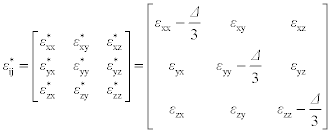
Third-generation synchrotron X-ray sources provide enough brightness for microdiffraction strain measurements with spatial resolution below 1 μm. Strain measurements for individual grains, or even within a single grain, are possible. Strain evolution measurements on Cu conductor lines during EM can be made for Cu lines with micrometer or submicrometer line widths. White beam X-ray Laue diffraction provides a method for measuring local deviatoric strain tensors εij∗, which are related to the usual full strain tensors εij
where Δ = εxx + εyy + εzz is the hydrostatic strain. For the usual choice of co-ordinate axes for thin film samples, εxx∗ and εyy∗ are the in-plane deviatoric strains and εzz∗ is the perpendicular deviatoric strain. The sum of the diagonal terms of the deviatoric strain tensor is zero,
In Laue microbeam X-ray diffraction, a CCD area detector is used to collect the Laue diffraction patterns. Figure 4.2 shows a Laue diffraction pattern from a single grain in a Cu thin-film sample. By analyzing the Laue patterns, the orientation and deviatoric strain tensor of each individual grain irradiated by X-rays, but not the hydrostatic strain, can be obtained. Detailed descriptions of analysis methods are available.6, 7
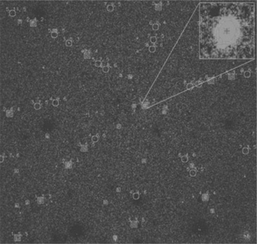
4.2 A Laue white beam X-ray diffraction pattern from a Cu grain, with an enlargement of the (333) Laue diffraction spot.5
4.2 Samples and X-ray microdiffraction methods
4.2.1 Copper conductor line samples
The Cu conductor lines used for microbeam X-ray strain measurements during EM described in this chapter were made by electrodeposition and patterned by the dual damascene process using chemical mechanical polishing (CMP).8 An optical image of a Cu line sample is shown in Fig. 4.3(a). On the same Si substrate, there are four identical sections of Cu lines, and each section contains three Cu lines in series. The Cu lines are 0.45 μm thick, 2 μm wide and 100 μm long, with dielectric and passivation layers. There are vias between each pair of Cu lines. The SiO2 passivation layer is 0.4 μm thick. A SEM image and schematic cross-section drawing of the Cu line are shown in Fig. 4.3(b) and 4.3(c). The grain size of the Cu line is similar to its thickness, ~ 0.5 μm.
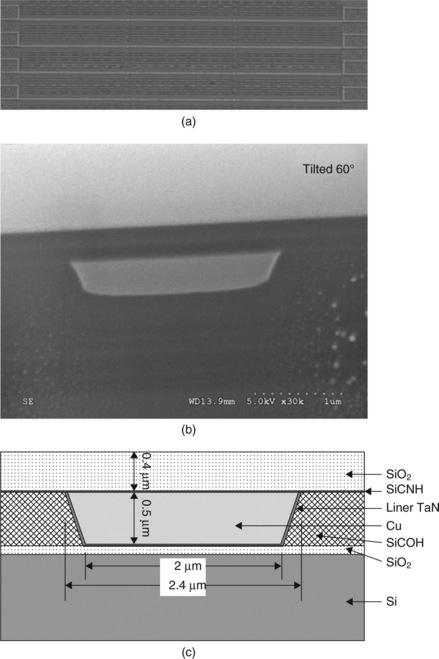
4.3 (a) Optical image of the Cu line sample.5 (b) SEM image of the cross-section of the Cu line after focused ion beam (FIB) milling.9 (c) Schematic sketch of the cross-section of the Cu line.10 (For (b) and (c): copyright © 2010 Materials Research Society. Reprinted with the permission of Cambridge University Press.)
4.2.2 X-ray microdiffraction experiments
Figure 4.4 shows a schematic of the experimental setup used at the Advanced Photon Source (APS) on beamline 34-ID. A photograph of the setup is shown in Fig. 4.5. Polychromatic X-rays from the synchrotron are focused by a set of K-B mirrors to form a microbeam of 0.5 μm diameter, which is diffracted from grains in the Cu line. The Cu line sample surface is oriented about 45 ° with respect to the incident X-ray beam. The CCD detector that collects the Laue diffraction patterns is above the Cu line sample, as shown in Fig. 4.4 and 4.5. The CCD and incident X-ray beam are fixed, and the sample stage is translated in directions along and across the Cu line, so that strain mapping of the entire Cu line is obtained. Cu fluorescence produced by the incident beam is used for sample alignment, as shown in Fig. 4.6.
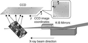
4.4 Schematic setup for X-ray microdiffraction experiments using a polychromatic X-ray beam.5
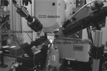
4.5 Setup of X-ray microbeam diffraction and heating stage.5
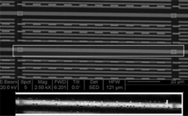
4.6 Top: SEM image of the Cu line; the white rectangle shows the area scanned by X-rays. Bottom: Cu fluorescence map showing where the X-rays are incident on the Cu line.5
4.2.3 X-ray microdiffraction strain measurement uncertainties
X-ray microdiffraction has been successfully applied to measure the strains for thin-film materials since 1998.11–15 However, few studies were focused on the measurement uncertainty. To estimate the measurement uncertainty using microbeam diffraction and Laue pattern indexing as described in 4.1, repeated strain mappings on the same Al conductor line, without EM, were carried out. Each strain mapping contains 1573 measurements along and across the line. The measurement uncertainty can be estimated as equation [4.3]
where Δε is the strain measurement uncertainty, λ11 is the self-correlation coefficient in the first strain mapping, λ22 is the self-correlation coefficient in the second strain mapping and λ12 is the correlation coefficient between the first and the second strain mappings. Detailed calculations for determination of the measurement uncertainty are shown in 4.6 Appendix. The calculated uncertainties are summarized in Table 4.1, with the uncertainties level ~ 2 × 10⁻⁴ for these strain measurements.
4.3 Electromigration (EM)-induced strains in conductor lines
4.3.1 Electron wind force and back flow strain gradient
Electromigration (EM) is the movement of atoms caused by current flowing in conductor lines. Atom movements are usually in the same direction as the electron flow. The driving force for the atomic diffusion is the electron flow, or electron wind force, in which the electrons transfer momentum to atoms.16 EM normally occurs at elevated temperature and high current density. Study of EM-induced strain is normally carried out at higher temperature and higher current density than the usual service conditions of integrated circuit devices, to allow the failure or significant strain evolution to develop and be measured in a reasonably short period of time. An expression for the atom flux J during EM, based on the initial proposal by Blech,17 is shown in equation [4.4]:
Deff is the effective diffusion coefficient,
k is the Boltzmann’s constant,
T is the absolute temperature,
Z* is the effective valency of the diffusing species,
ρ is the electrical resistivity of the conductor line,
∂σEM/∂x is the EM-induced stress gradient along the length of the conductor line, and
b is a stress state-dependent coefficient, with b = 2/3 if σEM is the equi-biaxial stress and b = 1 if σEM is the hydrostatic stress.11
For a conductor line with flux blocking boundaries at both ends and embedded in dielectric material, Blech proposed that there is a critical current density jc,17 and for currents below jc, that a stress gradient develops and eventually counterbalances the electron wind force, that the net atom flux then becomes zero, and that a linear stress gradient then extends over the full length of the conductor line. The effective valency Z* can be determined from the steady-state stress gradient (∂σEM/∂x) measured for a current density j below jc.
4.3.2 Role of passivation layers on the EM-induced strains
For insulation, antioxidation and dielectric purposes, dielectric materials and passivation layers are required in the interconnect technology. These passivation layers can greatly affect the strain evolution in conductor lines, because they confine the expansion or contraction of the lines. For ideal rigid confinement and bulk EM, the relationship between the change in local hydrostatic stress dσ and the change in local atomic density dC/C resulting from the atomic flux J is given by equation [4.5]:11, 17, 18
where B is bulk modulus of the conductor line and C is the number of atoms per unit volume in the conductor line. If the stress produced by the EM is equi-biaxial rather than hydrostatic, as expected for grain boundary EM in a wide, columnar film with weak vertical confinement, then B in equation [4.5] is the equi-biaixal modulus of the conductor line material. If the stress is uniaxial, as expected for top surface EM with strong vertical confinement, then B is the uniaxial modulus.
The passivation layer and surrounding dielectric materials play an important role in the magnitude of EM-induced strains, in which effective bulk modulus was used to replace B in equation [4.5]. Hau-Riege and Thompson18 used the finite-element method (FEM) to study the effect of the shape of the conductor line and the mechanical properties of the surrounding dielectric materials on the effective bulk modulus. Their results showed that with stiffer dielectric and passivation materials, the effective bulk modulus is larger and thus the EM induced stresses and strains are higher.18
4.3.3 Interplay between thermal and EM-induced strains
Because EM is usually studied at higher temperature and higher current density, thermal strain and EM-induced strains are both present during studies of EM-induced strain. Joule heating caused by high current density can contribute to thermal strain during the study of EM-induced strain. When the strain evolution has reached a steady state, the strain gradient predicted by equation [4.4] is a dynamic balance of atomic flux caused by EM, by the stress gradient and by thermal relaxation. For the study of pure EM-induced strain evolution in Cu conductor lines, Cu line samples are normally held at high temperature for sufficient time to allow the thermal strain to relax before the EM and X-ray strain measurements are started.
4.3.4 Measurements of EM-induced strains in Cu conductor lines
The Cu conductor line samples used in these measurements are described in 4.2.1. X-ray microbeam diffraction measurements were made at the Advanced Photon Source (APS) on beamline 34-ID. The X-ray beam was focused to about 0.5 μm diameter. Two Cu lines were chosen for EM testing with current flowing during the X-ray strain measurement, and two other Cu lines were chosen as control lines without current flowing, to compare with the EM test lines with the same fabrication and thermal history. The EM lines were stressed with a dc current of 2 mA, corresponding to a current density of 2.2 × 10⁵ A cm−2, and at a temperature of 270 °C.
Only deviatoric strains in three principal directions x, y and z were studied. Strains with positive signs are tensile, and strains with negative signs are compressive. A larger area than the Cu conductor line was scanned to make sure that all parts of the Cu lines were measured, as shown in Fig. 4.6. The total scan for the entire line took about 3 h. After each strain mapping of an EM line was completed, strain mapping of a control line was immediately made. The first measurement started after current has been flowing for 72 h in the EM-1 line at 270 °C and was completed 75 h after the start of EM. The scan of control line CL-1 was started at 75 h and completed at 78 h. After current had been flowing in the Cu EM lines for 120 h, strain mapping in EM-2 line was started and completed at 123 h. For 123 h to 126 h, strain mapping of the control line CL-2 was carried out.
Figure 4.7 shows the strain measurement results for lines EM-2 and CL-2. No strain gradient was found in EM-2 after current had been flowing for 120 h at 270 °C. However, there was a significant drop in the average strains in EM-2, compared with CL-2. Table 4.2 shows the average deviatoric strains in the x, y, z directions for the EM-1, CL-1, EM-2 and CL-2. From Fig. 4.7, the range of the strain values is also narrower in EM-2 compared with CL-2. The root mean square (RMS) variations of the strains for EM lines and for control lines are compared in Table 4.3. The flowing current significantly lowered the RMS values of the strains, making the strain distribution more uniform in the EM lines.
Table 4.3
Root mean square (RMS) deviations of the deviatoric strains in EM lines and control lines, in units of 10−3

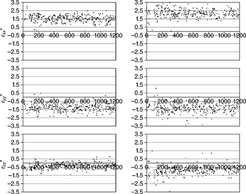
4.7 Left: Deviatoric strains in EM-2 line after 120 h of current stressing at 270 °C. Right: Line CL-2 after 123 h at 270 °C. The unit of strain is 10−3. The horizontal axis of the figure shows the X-ray measurement sequence, which is the same as the distance along the Cu line, with electron flowing from right to left side.10 (Copyright © 2010 Materials Research Society. Reprinted with the permission of Cambridge University Press.)
Because there is current flowing in the EM lines, the magnitude of Joule heating needs to be estimated, to determine whether greater strain relaxation in the EM lines may be simply a thermal effect. To estimate the temperature of the EM lines with the current density used in the EM study, the resistance of the EM lines was first measured at different temperatures using very small currents with negligible Joule heating, as shown in Fig. 4.8. The resistance of the Cu lines stabilized at 14.43 ohms when the current density was the same as the EM study. By fitting the curve in Fig. 4.8, the actual temperature of the Cu line during EM was estimated to be 272 °C. Without Joule heating, the temperature of the control lines should be the same as the heating stage temperature of 270 °C. The temperature difference of 2 °C between the EM lines and the control lines could not result in the strain relaxation, because the Cu diffusion coefficient changes insignificantly between 270 and 272 °C. Therefore, we conclude that EM is the dominant cause of the strain relaxation and strain homogenization observed in the Cu EM lines.
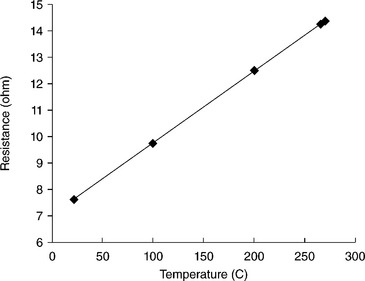
4.8 Resistance of Cu line at various temperatures, tested at low current with insignificant Joule heating.10 (Copyright © 2010 Materials Research Society. Reprinted with the permission of Cambridge University Press.)
4.3.5 Comparison of strain evolution for Al and Cu conductor lines
Strain evolution in Al conductor line with passivation layers has been reported by Wang et al.11 and Zhang et al.15 Both found that strain gradients formed during EM in the Al conductor lines. However, strain gradients along Cu conductor lines expected to develop during EM were not observed in direct strain measurements. Different mechanisms have been proposed for EM in Al and Cu conductor lines. In wide Al lines, the atomic diffusion path during EM is believed to be along the grain boundaries,11, 15 whereas in Cu, surface diffusion is the main diffusion path during EM.19 However, microstructure and line geometry are found to affect the EM mechanism. Mixture of grain boundary diffusion and surface diffusion are present in wide Cu conductor lines (more than 1 μm) with polycrystalline microstructure and surface diffusion dominates in narrower Cu conductor lines (less than 1 μm) with bamboo structures.20 Differences in the mechanical properties, as well as differences in electrical and thermal properties, between Al and Cu make the study of EM-induced strains in Cu materials more complicated than Al. For Cu there are many factors that could affect the strain evolution during EM, which need to be systematically studied. These factors include current density, temperature, grain structure, line geometry, and mechanical properties of the dielectric, liner and passivation layer materials. In our study of strain evolution in Cu conductor lines, although the current had been flowing in the EM lines for more than 120 h, the EM may be still at the early stage, which may explain why no strain gradient had yet formed along the line. Another possibility is that the current density used in this study may not have been high enough to produce a significant strain gradient, although it was sufficient for the electrons to interact with highly strained areas in the Cu lines to cause strain relaxation and strain homogenization.
4.4 Conclusions and summary
4.4.1 EM-induced strain relaxation in Cu conductor lines
The principles of synchrotron-based X-ray microbeam diffraction have been discussed, and results of measurements of deviatoric strains in Cu conductor lines have been described. No strain gradient was observed after EM for 120 h with a current density of 2.2 × 10⁵ A cm−2 at a temperature of 270 °C. However, the microbeam diffraction results show that EM has caused strain relaxation and strain homogenization in the Cu conductor lines, when compared with strain measurements in Cu conductor lines without current flowing.
4.4.2 Needs and opportunities for further work
Although much better EM resistance is expected in Cu interconnect materials than in Al, EM-induced failure is still one of the major concerns for the reliability of Cu-based IC devices. Because of the very different physical, mechanical, thermal and electrical properties between Cu and Al, strain caused by EM in Cu conductor lines cannot be simply understood or predicted based on the large amount of work carried out on EM behavior of Al conductor lines.
The EM mechanism in Cu conductor lines is not clearly established. The dependence of EM-induced strains on time, temperature, current density, microstructure, and mechanical properties of dielectric and passivation layer materials needs to be more systematically investigated. More reliable and efficient strain determination techniques, such as improved software to analyze the Laue patterns obtained during microbeam diffraction, are needed. Numerical modeling to explain the EM-induced strains remains challenging, as interconnect architectures become more and more complicated. Future research on the EM-induced strain and stress in Cu interconnects will provide valuable guidance for designing and fabricating more robust microelectronic devices.
4.5 References
1. Hu, C.-K. Electromigration failure mechanisms in bamboo-grained Al(Cu) interconnections. Thin Solid Films. 1995; 260:124.
2. Rosenberg, R., Edelstein, D., Hu, C.-K., Rodbell, K.P. Copper metallization for high performance silicon technology. Ann. Rev. Mater. Sci. 2000; 30:229.
3. Liu, R.F., Hu, C.-K., Gignac, L., Harper, J.M.E., Lloyd, J., Liu, X.-H., Stamper, A.K. Effects of failure criteria on the lifetime distribution of dual-damascene Cu line/via on W. J. Appl. Phys. 2004; 95:3737.
4. Nucci, J., Kramer, S., Arzt, E., Volkert, C.A. Local strains measured in Al lines during thermal cycling and electromigration using convergent-beam electron diffraction. J. Mater. Res. 2005; 20:1851.
5. Zhang, H., Thermal and electromigration induced strain and microstructure evolution in metal conductor linesPhD thesis. Lehigh University, 2009. [publication number 3358117].
6. Chung, J.-S., Ice, G.E. Automated indexing for texture and strain measurement with broad-bandpass X-ray microbeams. J. Appl. Phys. 1999; 86:5249.
7. Ice, G.E., Larson, B.C. 3D X-ray crystal microscope. Adv. Eng. Mater. 2000; 2:643.
8. Steigerwald, J.M., Murarka, S.P., Gutmann, R.J. Chemical Mechanical Planarization of Microelectronic Materials. Wiley-Interscience; 1997.
9. Zhang, H., Cargill, G.S., III., Maniatty, A.M. Thermal strains in passivated aluminum and copper conductor lines. J. Mater. Res. 2011; 26:633–639.
10. Zhang, H., Cargill, G.S., III. Electromigration induced strain relaxation in Cu conductor lines. J. Mater. Res. 2011; 26:498.
11. Wang, P.-C., Cargill, G.S., III., Noyan, I.C., Hu, C.-K. Electromigration-induced stress in aluminum conductor lines measured by X-ray microdiffraction. Appl. Phys. Lett. 1998; 72:1296.
12. Solak, H.H., Vladimirsky, Y., Cerrina, F., Lai, B., Yun, W., Cai, Z., IIlinski, P., Legnini, D., Rodrigues, W. Measurement of strain in Al–Cu interconnect lines with X-ray microdiffraction. J. Appl. Phys. 1999; 86:884.
13. Valek, B.C., Bravman, J.C., Tamura, N., MacDowell, A.A., Celestre, R.S., Padmore, H.A., Spolenak, R., Brown, W.L., Batterman, B.W., Patel, J.R. Electromigration-induced plastic deformation in passivated metal lines. Appl. Phys. Lett. 2002; 81:4168.
14. Spolenak, R., Barr, D.L., Gross, M.E., Evans-Lutterodt, K., Brown, W.L., Tamura, N., MacDowell, A.A., Celestre, R.S., Padmore, H.A., Valek, B.C., Bravman, J.C., Flinn, P., Marieb, T., Keller, R.R., Batterman, B.W., Patel, J.R. Microtexture and strain in electroplated copper interconnects. MRS Symp. Proc. 2000; 612:D1031.
15. Zhang, H., Cargill, G.S., Ge, Y., Maniatty, A.M., Liu, W. Strain evolution in Al conductor lines during electromigration. J. Appl. Phys. 2008; 104:1063.
16. Huntington, H.B., Grone, A.R. Current-induced marker motion in gold wires. Phys. Chem. Solids. 1961; 20:76.
17. Blech, I.A. Electromigration in thin aluminum films on titanium nitride. J. Appl. Phys. 1976; 47:1203.
18. Hau-Riege, S.P., Thompson, C.V. The effects of the mechanical properties of the confinement material on electromigration in metallic interconnects. J. Mater. Res. 2000; 15:1797.
19. Tu, K.N. Recent advances on electromigration in very-large-scale-integration of interconnects. J. Appl. Phys. 2003; 94:5451.
20. Hu, C.-K., Rosenberg, R., Lee, K.Y. Electromigration path in Cu thin-film lines. Appl. Phys. Lett. 1999; 74:2945.
4.6 Appendix
To estimate the measurement uncertainty in the determination of deviatoric strains using the Laue pattern-indexing technique as described in 4.2.3, two strain-mapping measurements were made on the same Al conductor line, held at 190 °C without electromigration. Each strain mapping contained 1573 points (an area scan of 13 × 121). The measured value at each location can be considered to consist of the sum of two parts, the true strain value plus a measurement error, which is related to the measurement uncertainty. In the estimation of uncertainties, two assumptions are made:
Assumption (1): At the same location, the true strain values for the two measurements are the same. The difference in results from the two measurements is caused by measurement error, related to measurements uncertainty, so
where ε1i(true) is the true strain, ε1i is the measured strain, and Δε1i is the measurement error at measurement location i (1 < i < 1573) for the first cycle of measurements. The corresponding values for the 2nd cycle of measurements are labeled with subscript 2.
Assumption (2): The average over strain measured for all measurement locations i for the 1st and 2nd cycles of measurements are nearly equal, because measurement errors are random and therefore uncorrelated, thus:
where <…> indicates averaging over all measurements.
The self-correlation function in cycle 1 is:
The self-correlation function in cycle 2 is:
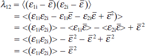
The correlation function between the two measurement cycles is:
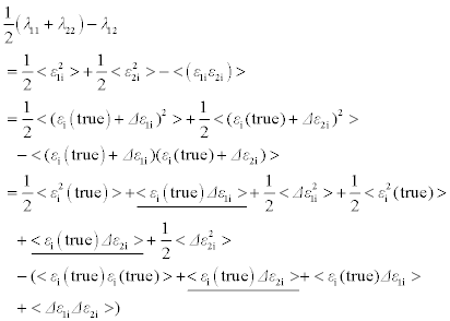
The difference between 1/2(λ11 + λ22) and λ12 is
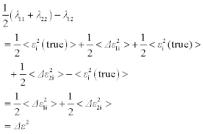
Since Δε1i and Δε2i are both random errors, the underscored terms in equation [4.11] are zero, when the number of measurement points are large enough. Equation [4.11] can be rewritten as:

