Scaling effects on electromigration reliability of copper interconnects
Abstract:
The effect of scaling on the electromigration (EM) reliability of Cu interconnects is investigated. First the intrinsic effect owing to scaling of the via and line dimensions is examined based on the dominant mass transport at the Cu top interface under EM. This is followed by a discussion of the extrinsic effects of processing-induced defects. EM results and failure modes are reviewed for both upstream and downstream electron flows, and the EM behaviors of multi-linked structures are discussed to further study the scaling effect. Methods of improving EM reliability are included and the results of using the CoWP cap are highlighted.
7.1 Introduction
The scaling of Cu interconnects continues to drive the reduction in via/line dimension and barrier thickness, with a concurrent increase in the current density. This has rendered electromigration (EM) a serious reliability concern for Cu interconnects. Beyond the 45 nm technology node, Cu damascene structures have two basic EM reliability issues. First, the scaling down of the line dimensions inherently reduces the EM lifetime because less material is required to induce the EM failure even if the current density remains the same. Second, the ratio of the interface to the volume of the interconnect structure continues to increase with scaling. These two factors reduce the time required for damage formation for future technology nodes assuming that the diffusion at the cap layer interface dominates the mass transport under EM (Hu et al. 1999, 2006, Hau-Riege and Thompson 2001, von Glasow et al. 2003). Hu et al. (2004, 2006) proposed a geometrical model to predict the scaling effect on EM lifetime taking into account the reduction of the critical void size and the line dimensions. The scaling effect on the EM lifetime is shown in Fig. 7.1 as a function of the cross-sectional area of the Cu line for each technology node (Hu et al. 2006). The open circles are the experimental data points and the solid line is the modeling prediction. The model predicts that the EM lifetime decreases by half for each new technology node, assuming that the current density remains the same. This is in good agreement with the observed EM lifetime degradation with scaling starting at 1 μm line dimensions. Given the fact that the actual current density continues to scale up for each technology node, the EM lifetime continues to degrade with scaling.
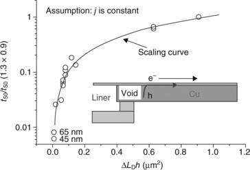
7.1 Normalized EM lifetime as a function of ΔLcrh (cross-sectional area wh) for various Cu interconnect generations (Hu et al. 2006).
In addition to the intrinsic effect of the dimensional scaling, there are extrinsic effects caused by processing-induced defects resulting from continuing interconnect scaling. In Cu interconnect, the vias connect the lower metal line to the upper metal line and are of particular concern as a weak link for reliability. The line/via structure with a high aspect ratio has been recognized as the most challenging issue for process integration. As the via dimensions shrink in each technology generation, both the via cross-sectional area and the surrounding barrier layer thickness are reduced. Processing difficulty in achieving thin and conformal barrier formation in via results in additional reliability issues arising from the barrier adhesion, integrity, and uniformity. In general, any defect at the via bottom can pose as a reliability weak point to limit the overall EM performance. In upstream EM tests, it is common to observe a bimodal EM lifetime distribution, in which the early failure mode (the weak mode) is caused by the void formation inside the via or at the via bottom (Fischer et al. 2002, Gill et al. 2002, Lee and Oates 2006, Lee et al. 2006, Li et al. 2004, Oates and Lee 2006). This failure mode is directly related to the via bottom processing, such as via etching, cleaning and barrier layer deposition. A slit-like void has been reported to form directly under the via bottom, resulting in an order of magnitude reduction in the EM lifetime (Lee and Oates 2006, Li et al. 2004, Oates and Lee 2006).
At the 65 nm node and beyond, with the Cu line width being scaled down below 90 nm, a polycrystalline grain structure or a mixture of bamboo and polycrystalline grain structures was reported (Hinode et al. 2001, Hu et al. 2007, Steinhogl et al. 2005, Zhang et al. 2007). Random line sections of polycrystalline grains were observed, especially at the trench bottom. In such Cu lines, the additional mass transport along the grain boundaries was found to further degrade the EM performance (Hu et al. 2007). As scaling continues, the surface-to-volume ratio of the Cu via and trench continues to increase, making it increasingly difficult to retain the bamboolike grain structures. For future technology nodes, more small grains are to be expected in the Cu lines, making it increasingly important to understand the effect of the scaling grain structures on EM reliability of Cu interconnects.
In this chapter, we review the studies on the scaling effect on EM reliability of Cu interconnects. First, we describe the nature of mass transport under EM in Cu interconnects and deduce the scaling effect on EM lifetime for the standard Cu interconnect where the mass transport is dominated by diffusion at the cap interface. This is followed by a review of the experimental studies on EM reliability and the effects of interconnect scaling for both downstream and upstream current flows. Via scaling is shown to play a key role in controlling the void formation and the EM lifetime, particularly for the downstream current flow. For the upstream current flow, there are two failure modes caused by void formation in the trench or at the via, which are identified by different resistance traces and by failure analysis using transmission electron microscopy (TEM). In the third section, the experimental studies on the early failure under EM as an important reliability predictor at the chip level, are reviewed. A statistical methodology has been developed using multi-linked test structures to measure the contribution of the early failure to the EM lifetime statistics. This method has been applied to EM tests for both upstream and downstream electron flows. Two distinct failure modes are observed and their effects on EM lifetime and statistics are discussed. Finally, the recent development of the cap layer interface to improve EM reliability by reducing the interfacial mass transport is reviewed. The CoWP cap is found to be particularly effective for improving EM performance. The results from a recent study on the CoWP cap are summarized and its effect on EM reliability for future technology nodes is assessed. Looking ahead, with interfacial diffusion being suppressed, grain structure will become increasingly important in contributing to the mass transport and in impacting EM reliability. The implications for future technological developments will be discussed.
7.2 Mass transport during electromigration (EM)
During EM, the atomic flux (Je) driven by the EM driving force (Fe) can be written as:
where n is the atomic density and vd is the drift velocity. The drift velocity of the moving metal ions can be expressed as:
where Deff is the effective diffusivity of the metal ions, Zeff∗e is the effective charge, ρ is the metal resistivity, kB is the Boltzmann constant, and T is the absolute temperature. Two parameters in equation [7.2] determine the drift velocity of metal ions and in turn the EM lifetime. The first is the current density j which continues to increase with the line scaling as specified by the ITRS roadmap (http://www.itrs.net/reports.html). The second is the effective diffusivity Deff of moving ions along various diffusion pathways. In Cu damascene structures, mass transport can occur through several fast diffusion pathways including the Cu/SiCN cap interface, the Cu/Ta liner interface and the grain boundary. The relative contributions from these pathways can be assessed from their activation energies. Those energies have been measured for Cu interconnects to be 0.7–0.95 eV for grain boundaries (Gupta 1988, Surholt et al. 1994, Surholt and Herzig 1997), 0.8–1.1 eV for the Cu/SiCN interface (Fischer et al. 2002a, Hu et al. 2002, Tokogawa et al. 2002) and 0.7–1.8 eV for the Cu/Ta liner interface (Demuynck et al. 2004, Hu et al. 2003, Lin et al. 2002). By comparison, the diffusion through the Ta liner interface is small and can be ignored. Accordingly, the parameter Zeff∗Deff can be expressed as:
where the subscripts identify the diffusion pathways by N as the Cu/SiCN interface and GB for grain boundary; δ is the width of the interface or the grain boundary, d is the grain size, and h is the line thickness. The parameter ƒ is a geometrical factor defined by the average orientation of the grain boundaries relative to the current flow. The parameters ƒ and d are statistical in nature, depending on the grain structure in the Cu line. For small grain polycrystalline structures, there is a higher proportion of grain boundaries aligned with the current flow, so the value of f/d is larger than the bamboo or near bamboo grains and contributes more to the mass transport. This is expected to be the case when the line width is scaled beyond the 65 nm node.
The EM lifetime is statistical in nature as it is related to the rate of damage formation at various flux divergence sites, which are statistically distributed. For simplicity, we consider a single damascene Cu line connected to a W via where the EM-induced void forms at the cathode end of the line. The EM lifetime τ can be written as (Hu et al. 2006):
where ΔLcr is the critical void length to cause the line failure under EM, which is approximately the via size. If the mass transport is dominated by the diffusion along the Cu/SiCN interface and the grain boundary, the EM lifetime can be expressed as:
For standard SiCN capped Cu interconnects with bamboo and near-bamboo grain structures, the parameter f approaches zero and can be neglected, thus the EM mass transport is dominated by the Cu/SiCN interface diffusion, with little grain boundary contribution. In this case, τ is directly proportional to ΔLcrh and inversely proportional to j. If the critical void size ΔLcr is about the same as the line width w, τ would be scaled with wh, the cross-sectional area of the line, or s2 with s being the scaling factor. For each technology generation, the line dimensions are scaled by a factor of ~ 0.7, which yields a reduction of ~ 50% in the EM lifetime. This trend has been confirmed by Hu et al. (2006) for Cu interconnects with the SiCN cap interface, and the results are shown in Fig. 7.1. In the above discussion, the local Joule heating is assumed to be negligible for the current density j used. In accelerated EM tests, the assumption may not hold; in that case, the j dependence can be more than linear.
7.3 Effect of via scaling on EM reliability
In 7.2, the effect of scaling of the via dimensions was discussed and the result showed that the effect is significant in that the EM lifetime decreases by half for each subsequent technology generation for a constant current density. Although this describes the intrinsic geometrical effect of via scaling, via processing for dual damascene structures is most challenging owing to the difficulty of forming thin and conformal barriers in vias with high aspect ratio, particularly for Cu/low-k interconnects. This raises a basic question concerning the effect of via processing in addition to the geometrical scaling on EM reliability.
A variety of test structures have been designed to study the EM lifetime and failure modes using either upstream electron flow (V1M2) or downstream electron flow (V1M1). Figure 7.2 shows the schematics of the test structures. Although the single-linked structures are used to study the basic failure mechanisms, multi-linked structures significantly increase the sample size, allowing the early failures to be observed. In this section, we discuss the results using such test structures to investigate the via scaling effects on EM reliability for Cu/low-k dual damascene interconnects.
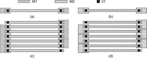
7.2 Schematic of EM test structures: (a) single-linked upstream, V1M2; (b) single-linked downstream, V1M1; (c) multi-linked upstream, V1M2, N = 10, 100; (d) multi-linked downstream, V1M1, N = 10, 100.
7.3.1 EM lifetime and failure mode with downstream electron flow
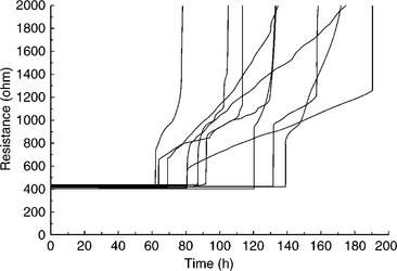
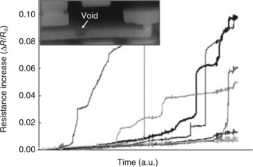
Stressing of single-linked EM structures with downstream electron flow from the upper to lower metal lines leads to either abrupt, large resistance increase or progressive monotonic resistance increases with the stress time. Typical examples are shown in Fig. 7.3. Examinations of the stressed vias reveal that the progressive resistance increases are associated with voids that are located either (a) at the cathode via, extending along the line length direction, or (b) in the trench away from the cathode via, as shown in Fig. 7.4(a) and 7.4(b). In both cases, the trench liner maintains electrical redundancy at the point of void formation. The abrupt resistance changes, however, result from void formation directly under the vias, where the void is in the shape of a narrow slit, as shown in Fig. 7.4(c). The only variations in this failure mode seems to be the extension of the void in front of the via, and a small variation in the void depth below the via.
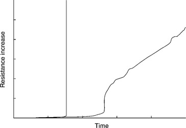
7.3 Progressive and abrupt resistance increases for typical single-linked downstream EM test structures.
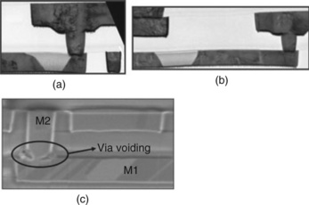
7.4 TEM/FIB images of void formation for downstream electron flow: (a) at the cathode via, extending along the line direction; (b) in the trench away from the cathode via; (c) directly under the vias, where the void is in the shape of a narrow slit.
The various void locations can induce different critical failure void volumes, as shown in Fig. 7.4. If a void nucleates directly under the via, the effect of the line width on the EM lifetime are mediated through the scaling of the via size. This is confirmed by the downstream EM tests performed on single-linked Ml Cu lines with the line widths of 125 and 175 nm, where the Ml line width is the same as the V1 via size. Fig. 7.5 shows the EM test results, where the 175 nm lines exhibit a longer EM lifetime than the 125 nm lines. The EM lifetime was found to scale with the M1/V1 size, which can be attributed to the scaling of the critical void size ΔLcr. The failure mechanism is confirmed by focused ion beam (FIB) cross-sectioning analysis of failed samples. A typical large void under the via at the cathode end is observed (Fig. 7.6) where Cu atoms are completely depleted.
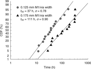
7.5 CDF plots of single-linked downstream EM tests of 125 and 175 nm wide M1 lines. The EM tests were performed at T = 270 °C, with j=1.0 MA cm−2.
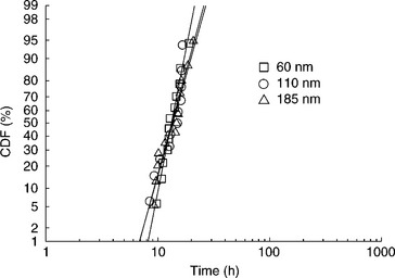
On the other hand, if a void starts to nucleate in the M1 trench away from the via, the scaling effects of the line width on the EM lifetime can be diminished. This is demonstrated in the EM test results of the single-linked V1M1 structures with different line widths of 60, 110, and 185 nm, as shown in Fig. 7.7. The cumulative distribution function (CDF) plots reveal that the EM lifetime distribution is independent of the Ml line widths employed. The reasoning behind the line width independence is explained in the following. Because the void-induced EM failure is found to form in the Ml trench, the critical void size ΔLcr remains constant, independent of the line width. The EM lifetime then depends solely on the metal line thickness h. Because the line thicknesses for test samples with different line widths are identical, the lifetimes become the same under the same temperature and current density conditions, as shown in Fig. 7.7.
7.3.2 EM lifetime and failure mode with upstream electron flow
The CDF plots obtained from the EM tests with upstream current flow are shown in Fig. 7.8 for three V1/M2 sizes of 90, 125, and 175 nm. In this study, all the line structures have the same cap layer interface and line thickness and are tested under the same conditions, thus the EM lifetime is expected to be directly correlated to ΔLcr. The line fails owing to void growth starting from the cathode end of the trench to span over the whole via. In this case, ΔLcr is proportional to the via size and thus the EM lifetime should scale with the via width. This is in good agreement with the results shown in Fig. 7.8.
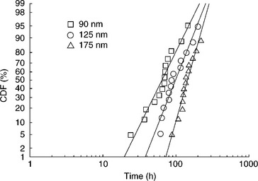
7.8 CDF plots of single-linked upstream EM tests of 90, 125 and 175 nm wide M2 lines. EM tests were performed at T = 330 °C, with j =1.0 MA cm−2.
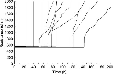
The resistance traces recorded during the EM test for the 125 nm test structures are plotted in Fig. 7.9. The resistance changes showed a typical intrinsic EM failure behavior where the first abrupt resistance increase occurs when a void growing from the cathode end covers the whole via. The current is then shunted to the Ta barrier, causing the resistance to abruptly increase. The subsequent gradual increase in resistance is the result of continuing void growth along the M2 trench. When the Ta barrier can no longer sustain the current density, the barrier burns out to cause a final abrupt increase in resistance.
In contrast, the resistance traces for the 90 nm wide lines exhibited both gradual and abrupt increases as shown in Fig. 7.10. The abrupt resistance increase is attributed to either via bottom voiding or trench voiding caused by extrinsic process-induced defects. The gradual increase is attributed to the same intrinsic failure mode as described for the 125 nm lines. The combination of the two failure modes leads to a wider lifetime distribution for the 90 nm lines than the 125 and 175 nm lines, as shown in Fig. 7.8.
One of the 125 nm wide EM-failed samples is analyzed using FIB, and the image is shown in Fig. 7.11. Even though the via structure cannot be clearly discerned owing to severe joule heating, a large trench void at the cathode end is evident. This damage mode supports the intrinsic failure mechanism owing to void formation at the cathode driven by interfacial mass transport. This is also consistent with the resistance traces shown in Fig. 7.9.
7.4 Multi-linked statistical tests for via reliability
The previous discussion was focused on the EM tests performed on the single-linked EM test structures. Both types of resistance increases, abrupt and progressive changes, are observed in the single-linked structures. To assess the EM reliability at the chip level where millions of Cu lines are connected, it is essential to develop a method to determine the rate of the early failures. For this purpose, multi-linked test structures are designed for measuring the early failure statistics and two examples of multi-linked test structures for upstream and downstream current flow are shown in Fig. 7.2(c) and 7.2(d). In EM tests, multi-linked test structures with different number of links, N = 1, 10 and 100 for example, are used for statistical determination of different failure modes. The multi-linked structures greatly increase the number of test structures and thus significantly increase the probability of detecting the early failures.
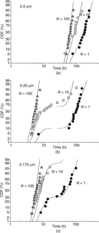
The multi-linked test structures are designed for quantitative data analysis to determine the proportions of the failure modes and EM statistics. The analysis is based on the ‘weakest link approximation’ (WLA) statistics in combination with the Monte Carlo simulation (Lee et al. 2004, Ogawa et al. 2001). This method has been applied to study the scaling effect on via reliability with the upstream electron flow. The CDF plots of the upstream multi-linked structures with N = 1, 10, and 100 from the experiments and the subsequent weakest link approximation (WLA) Monte Carlo simulation are presented in Fig. 7.12 as a function of the line width. Solid symbols are the actual lifetime data from the experiment and the lines with small dots represent the results generated by Monte Carlo simulations. The branching caused by the bimodal failure mechanism in the data is readily observed for both the 0.25 μm and the 0.175 μm structures. With the Monte Carlo simulation for the best fitting curves based on the WLA, even the results of the 0.5 μm structures reveal both the strong failure and the weak failure modes. Together with the simulations, the average lifetime t50, standard deviation σ, and the failure population for the strong and the weak modes can be determined and the results are listed in Table 7.1. The EM lifetime of the intrinsic strong mode shows a systematic linear decrease with the line width scaling. This can be attributed to the decrease of the critical void size with line/via width as discussed above. It is interesting to note that the weak via-related failure mode lifetimes are not simply related to the change of the line width; instead, they are more closely related to the extrinsic process-induced defects, such as poor barrier coverage at the via bottom. As the linewidth decreases, processing control becomes more difficult and challenging. This is reflected in the increase of the proportion of the weak mode and the decrease in the lifetime of the weak mode for the 0.25 and 0.175 μm test structures.
7.5 Methods to improve the EM lifetime
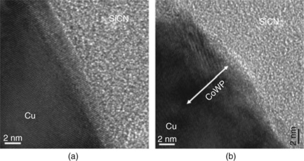
The reliability concern for Cu interconnects with scaling has generated significant interest recently in developing methods for improving the EM reliability. These include the use of Cu surface alloying, the formation of a CuSiN top layer, and the formation of a metal cap layer underneath the SiCN passivation layer. The use of a metal cap layer, such as CoWP, CuSnP, Pd, Ta and Ru, was found to be most effective in suppressing the cap interface diffusion. Figure 7.13 compares the CDF plots of the downstream EM tests for Cu interconnects with SiCN cap and CoWP cap. The test structures are fabricated by using the 45 nm technology process with test line width of 80 nm and line height of 144 nm. The EM results show that compared with the SiCN cap, the CoWP cap improves the EM lifetime of the Cu interconnects by ~160 times with an increase in σ from 0.30 to 0.88. Only four of the CoWP capped Cu lines failed when the test was terminated even after a long period of current stressing. The improvement of the EM lifetime for the CoWP cap is the result of the reduction in the Cu/cap interface diffusion, which can be attributed to the highly ordered crystalline interface between Cu and CoWP (Meyer and Zschech 2007), as well as the much higher bonding strength between Cu and Co compared with that between Cu and amorphous SiCN (Lane et al. 2003). The difference in the interface crystalline quality is demonstrated in Fig. 7.14 using high-resolution TEM (HR-TEM) analysis along the Cu/SiCN and Cu/CoWP interfaces. It can be seen that the Cu line has a sharp interface with the SiCN cap, which has no distinct crystalline features. In contrast, for the Cu/CoWP interface, almost perfect crystalline planes of Cu extend all the way through the CoWP metal cap with no distinguishable interface in between. This indicates that the Cu/CoWP interface is characterized by highly ordered crystalline structures with strong bonding strength to suppress the interface diffusion.
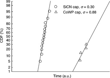
7.13 CDF plots of the M2 Cu interconnects with different caps: SiCN versus CoWP. EM tests were performed at T = 330 °C, with j =1.0 MA cm−2.
Failure analyses by FIB and TEM observations show that for the SiCN-capped Cu lines, voids form either at the cathode via corner extending along the Cu line direction, or in the trench a certain distance away from the cathode via. For the SiCN capped lines, different failure locations show corresponding resistance changes: via corner voiding corresponds to a relatively small initial resistance increase, whereas the trench voiding corresponds to a large initial resistance change, as shown in Fig. 7.15 and 7.16. In comparison, for the CoWP capped Cu lines, voids mostly form in the trench away from the cathode via, irrespective of the amount of the initial resistance step, as shown in Fig. 7.17. The difference in the voiding locations for these two cap layers can be attributed to the difference of the interface diffusion. For the SiCN cap, the cap interface diffusivity is large, so voids can move readily along the interface and eventually accumulate at the cathode via corner to fail the line. In contrast, for the CoWP capped Cu lines with interface diffusion effectively suppressed, voids can easily get trapped at locations with either an interface defect or a large grain triple junction. The trapped voids grow in the trench away from the cathode via, eventually causing the line to fail under EM.
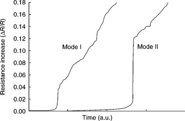
7.15 Typical resistance traces of mode I and mode II failures: mode I with a small initial resistance increase and mode II with a large initial resistance jump.
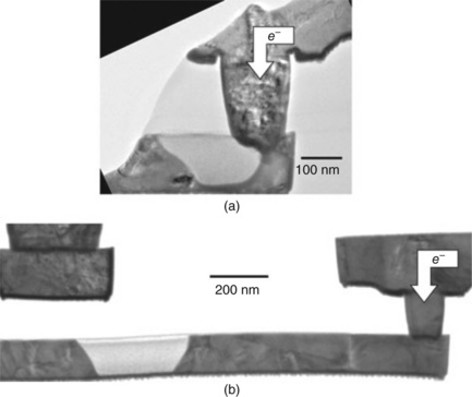
7.16 Cross-sectional TEM images of EM failed samples showing different voiding locations: (a) at the via corner; (b) in the trench away from the via, corresponding to mode I and mode II failures in Fig. 7.15, respectively.
7.6 Conclusion and future trends
In this chapter, we have discussed the via scaling effects on EM reliability for Cu interconnects. First we examined the intrinsic effect of scaling of the via and line dimensions based on the dominant interface mass transport under EM. The intrinsic effect was found to be significant, resulting in a decrease of EM lifetime by half for each technology node even with a constant current density. This was followed by a discussion of the extrinsic effects of processing-induced defects which were traced to the difficulty of processing the dual damascene structure. Such defects can significantly degrade the EM lifetime and statistics. To investigate the via scaling effects, a variety of test structures were designed, including single-linked and multi-linked structures. EM test results and the characteristics of the failure modes are discussed for both upstream and downstream electron flows. Finally, we summarized the method of using a metal cap layer to improve EM reliability and highlighted the results of the CoWP capping layer.
To conclude this chapter, we examine the scaling effect by projecting the EM performance for the CoWP technology. For this purpose, the EM lifetime is expressed as:
The g factor, defined as the ratio of the mass transport through the grain boundary vs. the cap interface, can be expressed as:
Equation [7.6] is written in a format to facilitate the discussion of cap layer and grain structure effects on EM lifetime. According to equation [7.6] and the model proposed by Hu et al. (2006), the ratio of the median lifetime for each technology node relative to that of the 0.13 μm technology is plotted in Fig. 7.18 as a function of the critical void volume ΔLcrh (or the cross-sectional area wh). Both grain boundary and interfacial diffusion contributions to mass transport are included here. For standard SiCN capped Cu interconnects with bamboo or near-bamboo microstructures, the f term approaches to zero and can be neglected, thus the EM mass transport is primarily controlled by diffusion at the Cu/SiCN interface. For each technology node, if we assume the current density j remains the same, the EM lifetime degrades by half owing to the scaling of the geometrical factor ΔLcrh (wh), as shown by the reference line ‘1’ in Fig. 7.18. However, when the CoWP metal cap is used, the atomic diffusion along the interface is significantly suppressed, resulting in a reduction of DN by a factor of 40 ~160 depending on the metal cap process (Zhang et al. 2010). The scaling curve shifts up significantly as shown by line 3 in Fig. 7.18, where we assume a 40 × lifetime improvement for demonstration.
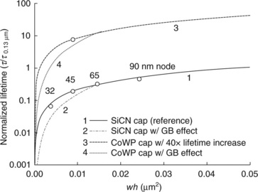
7.18 Normalized EM median lifetime versus wh (cross-sectional area) for various Cu interconnect generations considering different dominant Cu diffusion paths. The data points of open circle are experimental data based on this study and the results provided by GLOBALFOUNDRIES.
As scaling continues, more small grains emerge in the Cu lines after the 65 nm node, and a higher proportion of grain boundaries are aligned with the current flow. This causes an increase in f with a smaller d, resulting in an overall increase of the fgh/d term. Thus, the grain boundary diffusion becomes increasingly important, which, in turn, accelerates the mass transport under EM and degrades the EM performance, as illustrated by the dashed line labeled as ‘2’ in Fig. 7.18. The presence of small grains can have a larger impact on the EM lifetime for structures with CoWP capping, as reported by Zhang et al. (2010). This is because the suppression of interfacial diffusion by the CoWP cap causes the grain boundary diffusion to become more dominant in controlling the mass transport. Consequently, a small change in the grain structure can yield a large change in the overall Cu diffusivity as well as the EM lifetime. Nevertheless, the benefit of the CoWP cap over the SiCN cap remains significant even for the 32 nm technology node, as evidenced by comparing line 2 and line 4. To ensure EM reliability for the 22 nm technology node and beyond, the grain structure must be optimized together with the cap layer process.
In the above estimate of the scaling effect, we use a simple approach by treating the effect of the grain structure on EM lifetime as an average of the grain size and orientation. In reality, the problem is considerably more complicated and inherently statistical in nature. This can be seen from the results shown in Fig. 7.13 where the standard deviation σ increases from 0.30 for the SiCN cap to 0.88 for the CoWP cap for the same Cu grain structure. This suggests that the EM characteristics, particularly its statistics, depend not only on the average grain structure but also on the coupling between the mass transport along the grain boundary and the cap interface in forming the voids which lead to the EM failure. This raises interesting questions for future studies.
7.7 Acknowledgements
The authors are grateful for the funding support from the Center for Advanced Interconnect Science and Technology of the Semiconductor Research Cooperation (SRC/CAIST) and for the Cu test structures provided by L. Smith and G. Smith from Sematech, and O. Aubel and C. Hennesthal from the Globalfoundries in Dresden, Germany.
7.8 References
Demuynck, S., Tokei, Z.S., Bruynseraede, C., Michelon, J., Max, K. Advances in Metallization Conference. 2004; 355.
Fischer, A.H., von Glasow, A., Penka, S., Ungar, F. Electromigration failure mechanism studies on copper interconnects. IEEE International Interconnect Technology Conference Proceedings. 2002; 139–141.
Gill, J., Sullivan, T., Yankee, S., Barth, H., von Glasow, A. Investigation of via-dominated multi-modal electromigration failure distributions in dual damascene Cu interconnects with a discussion of the statistical implications. IEEE International Reliability Physics Symposium Proceedings. 2002; 298–304. [Dallas, TX].
Gupta, D. Diffusion phenomena in thin films and microelectronics materials. In: Gupta D., Ho P.S., eds. Chapter 1. Park Ridge, NJ: Noyes, 1988.
Hau-Riege, C.S., Thompson, C.V. Electromigration in Cu interconnects with very different grain structures. Applied Physics Letters. 2001; 78:3451–3453.
Hinode, K., Hanaoka, Y., Takeda, K., Kondo, S. Resistivity increase in ultrafine-line copper conductor for ULSIs. Japanese Journal of Applied Physics, Part 2: Letters &Express Letters. 2001; 40:1097–1099.
Hu, C.K., Canaperi, D., Chen, S.T., Cignac, L.M., Herbst, B., Kaldor, S., Krishnan, M., Liniger, E., Rath, D.L., Restaino, D., Rosenberg, R., Rnbino, J., Seo, S.-C., Simon, A., Smith, S., Tseng, W.T. Effects of overlayers on electromigration reliability improvement for Cu/low k interconnects. IEEE International Reliability Physics Symposium Proceedings. 2004; 222–228.
Hu, C.K., Gignac, L., Liniger, E., Herbst, B., Rath, D.L., Chen, S.T., Kaldor, S., Simon, A., Tseng, W.T. Comparison of Cu electromigration lifetime in Cu interconnects coated with various caps. Applied Physics Letters. 2003; 83:869–871.
Hu, C.K., Gignac, L., Rosenberg, R. Electromigration of Cu/low dielectric constant interconnects. Microelectronics Reliability. 2006; 46:213–231.
Hu, C.K., Gignac, L., Liniger, E., Rosenberg, R., Stamper, A. Bimodal electromigration mechanisms in dual-damascene Cu line/via on W. IEEE International Interconnect Technology Conference Proceedings. 2002; 133–135. [Burlingame, CA].
Hu, C.K., Gignac, L., Baker, B., Liniger, E., Yu, R., Flaitz, P. Impact of Cu microstructure on electromigration reliability. IEEE International Interconnect Technology Conference Proceedings. 2007; 93–95. [Burlingame, CA].
Hu, C.K., Rosenberg, R., Lee, K.Y. Electromigration path in Cu thin-film lines. Applied Physics Letters. 1999; 74:2945.
Lane, M.W., Liniger, E.G., Lloyd, J.R. Relationship between interfacial adhesion and electromigration in Cu metallization. Journal of Applied Physics. 2003; 93:1417.
Lee, K.D., Ho, P.S. Statistical study for electromigration reliability in dual-damascene Cu interconnects. IEEE Transactions on Device and Materials Reliability. 2004; 4:237–245.
Lee, K.D., Park, Y.J., Kim, T., Hunter, W.R. Via processing effects on electromigration in 65 nm technology. IEEE International Reliability Physics Symposium Proceedings. 2006; 103–106.
Lee, S.C., Oates, A.S. Identification and analysis of dominant electromigration failure modes in copper/low-k dual damascene interconnects. IEEE International Reliability Physics Symposium Proceedings. 2006; 107–114. [San Jose, CA].
Li, B., Sullivan, T.D., Lee, T.C., Badami, D. Reliability challenges for copper interconnects. Microelectronics Reliability. 2004; 44:365–380.
Lin, J.C., Park, S.K., Pfeifer, K., Augur, R., Blaschke, V., Shue, S.L., Yu, C.H., Liang, M.S. Electromigration reliability study of self-ionized plasma barriers for dual damascene Cu metallization. Advances in Metallization Conference. 2002; 233–237.
Meyer, M.A., Zschech, E., New microstructure-related EM degradation and failure mechanisms in Cu interconnects with CoWP coating. AIP Proceedings of the International Workshop Stress Induced Phenomena in Metallization. Kyoto, Japan, 2007:107.
Oates, A.S., Lee, S.C. Electromigration failure distributions of dual damascene Cu/low-k interconnects. Microelectronics Reliability. 2006; 46:1581–1586.
Ogawa, E.T., Lee, K.D., Matsuhashi, H., Ko, K.S., Justison, P.R., Ramamurthi, A.N., Bierwag, A.J., Ho, P.S., Blaschke, V.A., Havemann, R.H. Statistics of electromigration early failures in Cu/oxide dual-damascene interconnects. IEEE International Reliability Physics Symposium Proceedings. 2001; 341–349.
Steinhogl, W., Schindler, G., Steinlesberger, G., Traving, M., Engelhardt, M. Comprehensive study of the resistivity of copper wires with lateral dimensions of 100 nm and smaller. Journal of Applied Physics. 2005; 97:023706–023712.
Surholt, T., Herzig, C. Grain boundary self-diffusion in Cu polycrystals of different purity. Acta Materialia. 1997; 45:3817–3823.
Surholt, T., Mishin, Y.M., Herzig, C. Grain-boundary diffusion and segregation of gold in copper: Investigation in the type-B and type-C kinetic regimes. Physical Review B. 1994; 50:3577.
Tokogawa, S., Takizawa, H. IEEE International Interconnect Technology Conference Proceedings. 2002; 127.
Von Glasow, A., Fischer, A.H., Bunel, D., Friese, G., Hausmann, A., Heitzsch, O., Hommel, M., Kriz, J., Penka, S., Raffin, P., Robin, C., Sperlich, H.P., Ungar, F., Zitzelsberger, A.E. The influence of the SiN cap process on the electromigration and stressvoiding performance of dual damascene Cu interconnects. IEEE International Reliability Physics Symposium Proceedings. 2003; 146–150.
Zhang, L., Zhou, J.P., Im, J., Ho, P.S., Aubel, O., Hennesthal, C., Zschech, E. Effects of cap layer and grain structure on electromigration reliability of Cu/low-k interconnects for 45 nm technology node. IEEE International Reliability Physics Symposium Proceedings. 2010; 581–585. [Anaheim, CA].
Zhang, W., Brongersma, S.H., Li, Z., Li, D., Richard, O., Maex, K. Analysis of the size effect in electroplated fine copper wires and a realistic assessment to model copper resistivity. Journal of Applied Physics. 2007; 101:063703–063803.


