Electromigration in flip-chip solder joints
Abstract:
This review is devoted to four types of physical failure mechanisms in microelectronic devices for high-current density applications; those failures are electromigration (EM), Joule heating-induced failures, stress-related damage, and thermomigration (TM). In practice, some of these failure mechanisms occur together so that the real root cause cannot easily be detected and understood. Reliability designers need to be well informed to evaluate the electrical characteristics, thermal characteristics and mechanical strength for solder interconnects in advance. Recent progress in failure mechanism evaluation is summarized and a critical overview of the basis of atomic transport, diffusion kinetics, morphological evolution, and numerical simulation is presented. Special emphasis is on the understanding of EM interactions with other failure mechanisms. In addition to this review of the current knowledge, the remaining challenges as well as future directions are also discussed.
10.1 Introduction
10.1.1 Solder interconnects for advanced electronic packaging
With the trend towards higher integration and further miniaturization of Si-based devices, electronic packaging is successively requiring a higher input/output (I/O) density, smaller feature size, and better performance. Concurrently, the flip-chip solder interconnect has established its leadership role for high current density packages, as thousands of solder bumps are fabricated onto one single chip. To meet an even higher demand for device performance, the I/O number is expected to increase, whereas the dimensions of each individual bump will accordingly need to shrink.
According to the 2003 International Technology Roadmap for Semiconductors (ITRS), a significant downsizing in flip-chip packaging is anticipated.1 Figure 10.1 shows the anticipated variation in pad diameter, pad pitch and line width. In addition, the bump size is expected to reduce along with the pad size and pitch. At present, the diameter of a solder bump in use is about 100 μm or less.2 In 2007, the diameter of micro-bumps had been decreased to 20 μm.3 This persistent scaling-down inevitably places severe challenges on the reliability of micro-devices, as discussed later.
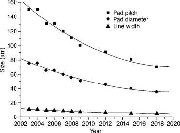
10.1 A downsizing in flip-chip packaging, based on 2003 ITRS edition.1
10.1.2 Challenges of high current density applications
At present, in the microelectronic industry, each solder joint is designed to carry 0.2 A, and the current will be doubled in the near future.2 Therefore, the average current density through a 50 μm diameter solder joint may approach 104 A cm−2. This demands a reduced cross-section of the conductive lines and solder interconnects, in spite of the fact that these structures are expected to conduct such a high current density. Meanwhile, because Joule heating is proportional to the square of the current density, the local temperature of conductive lines and solder bumps rises substantially. Also, during field service, the solder joints experience a temperature rise of at least 100 °C, to approximately 82 and 76% of the melting temperatures of eutectic SnPb and SnAgCu, respectively. As a consequence, under the combined effect of a high current density and a high homologous temperature, efficient diffusion of atoms in the lattice is anticipated.4 This renders electromigration (EM) a serious reliability issue in the application of high current density packages.
EM is defined as a diffusion-controlled mass transport phenomenon owing to the application of electrical current. In 1961, Huntington and Grone proposed that a thermally activated metal ion becomes essentially free in the lattice and is acted upon by two opposing forces (a direct force and an electron wind force) in a metal.5 Also, Huntington and Grone identified the electron wind force as the primary driving force responsible for the EM failure observed in interconnects. The electron wind force is further explained as one force experienced by a metal ion in the direction of the electron flow owing to the momentum exchange between the moving electrons and the ion. Therefore, the phenomenological equation for the atomic flux due to EM (Jem) is described as:
where Z* is a dimensionless quantity known as the effective charge or the effective valence that reflects the direction and magnitude of the momentum exchange, e is the electron charge, E is the electric field, ρ is the resistivity, j is the current density, C is the concentration of diffusing atoms, v is the drift velocity of these atoms, D is the thermally-activated diffusivity, and kT is the average thermal energy.
Regarding the EM of tin and lead in solder alloys, Brandenburg and Yeh first published research in 1998.6 EM causes the net atom transport of solder material along the direction of the electron flow. Since 2002, ITRS has started to include this reliability problem for industrial attention.7 Table 10.1 lists the near-term reliability challenges requiring concern in current assembly and packaging techniques.3 According to the 2007 ITRS, EM becomes a more limiting factor of high current density packages, such as wafer-level packaging (WLP) for micro-electro-mechanical systems (MEMS). It is suggested that physical failure mechanisms such as EM, and thermal migration in combination with mechanical stresses, should be understood and modeled for practical life assessment. In particular, solder and the under bump metallurgy (UBM) need to be well designed to support a high current density and minimize or avoid EM.
Also, thermal dissipation is addressed as a critical factor of reliability considering the large Joule heating generated by the on-chip metal interconnects. One should appreciate that the cross-sectional area of conductive lines on the chip has been decreased significantly with the trend towards miniaturization, as shown in Fig. 10.1. It is true to say that the on-chip interconnects used in electronic packages may be based on Al or Cu materials. However, most concern is with interconnects based on Al, where Joule heating is more pronounced (the resistivity of Cu is about 60% of that of Al). For a flip-chip interconnect, the electrical resistance of the Al traces is at least one order of magnitude higher than that of the solder joints and Cu conductors, and thus the Al traces are the primary heat source. A significant Joule heating will accelerate the EM process in the neighboring solder joints, but also result in the degradation of UBM layers and even the Al trace itself.
Another concern is the formation of compression and tension regions inside a solder joint, when atoms are driven from the cathode to the anode by the electron wind force. Stress generation and relaxation are issues under exploration, and stress-related damage under a current density should be paid considerable attention. In addition, mechanical properties are direct indicators of strength and long-term durability. It is understandable that EM would exert a certain effect on the mechanical transition of solder interconnects. As an important reliability factor, the mechanical behavior of solder interconnects for high current density applications also needs to be carefully considered.
Moreover, owing to the significant heat accumulation, the atomic migration process, thermomigration (TM), may be triggered and influence the reliability of packages. Owing to differences in electrical resistance and thermal dissipation of individual parts within the flip-chip interconnect structure, it is predicted that the heat accumulated at the chip side will be larger than that at the substrate side. This variation inevitably leads to a considerable temperature gradient across solder joints, which can provide a driving force for atomic diffusion to trigger TM. More exactly, the driving force of TM comes from both the energy transported by the moving atoms and the interactions with the usual heat carriers in the lattice.8 The phenomenological equation for the atomic flux owing to TM (Jtm) is:9
where Q* is the heat of transport and is the heat flow per mole that must be supplied to maintain unit molar flow in the steady state, N is Avogadro’s number, and ΔT is the thermal gradient. The other terms in the above equation have been defined under equation [10.1]. Being a potential reliability concern for flip-chip solder interconnects, TM induced-void or pore formation has also been introduced in the 2007 ITRS.3
10.1.3 Scope of this review
During field service, all the factors discussed are supposed to combine and act concurrently, thus further complicating the failure processes. Therefore, a quantitative understanding of the physics and mechanics of each failure mechanism strengthens the design and life prediction in flip-chip solder interconnects, which is of particular interest to both those in industry and in academia.
Four types of failure mechanism are presented in this review. Section 10.2 addresses the void formation during EM in solder interconnects. In addtion, from an engineering standpoint, this section summarizes the lifetime statistics and reliability evaluation of EM of solders. Section 10.3 reviews the dissolution of the UBM owing to an accelerated interstitial diffusion, and the diffusion of on-chip Al trace under Joule heating, then introduces research results on the time-dependent melting behavior of solder interconnects under current stressing. A summary of stress-related degradation in solder interconnects is presented in section 10.4. The morphological evolution owing to EM and the back stress induced are described. Also some mechanical deformation and degradation mechanisms under current stressing are summarized as a part of an overall understanding of the mechanical behavior. Section 10.5 discusses the reliability concerns of TM. The thermo-transports of Pb, Sn, Cu and Bi in solder interconnects under a thermal gradient are introduced. Lastly, but importantly, issues that need to be investigated in the near future are proposed in section 10.6.
10.2 Electromigration (EM)-induced voiding failure of solder interconnects
10.2.1 Nucleation and growth of voids at the interface
During EM, atomic diffusion-induced microstructural evolution includes not only phase separation6,10–16 and phase coarsening,17–20 but also void creation at interfaces. Figure 10.2 displays the progress of void growth in Sn3.5Ag1.0Cu solder joints under a current density of 1.5 × 10⁴ A cm−2 at 125 °C.14 Figure 10.2a shows the typical morphology of the interface before the experiment. After a stressing time of 75 h, as shown in Fig. 10.2b, voids were initiated from the upper-right corner, and gradually displaced the current to the surrounding areas, resulting in a lateral growth. Because the growth of voids induced the redistribution of the current, it is also reasonable to find that the voids were developed towards the periphery of the UBM opening, where the original current density was low. This experimental finding verifies the finite element simulation by Liang et al.21 Figure 10.2c shows the microstructural development after 280 h. It is evident that the voids continuously extended from the right-hand to the left-hand regions. Figure 10.2d displays further void growth after 425 h. The propagation of voids decreased the effective contact area of the current path and induced a more serious current crowding, and thus accelerated the void growth along the interface. This process continued until the voids finally spread across the complete contact window at 515 h, as shown in Fig. 10.2e.
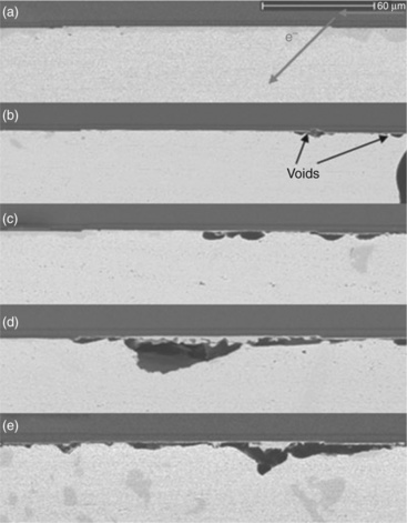
10.2 SEM images of the morphological evolution in Sn3.5Ag1.0Cu solder joints under a current density of 1.5 × 10⁴ A cm−2 at 125 °C (a) before the experiment, time point A, (b) after 75 h, 14% of the failure time, time point B, (c) after 280 h, 53% of the failure time, time point C, (d) after 425 h, 81% of the failure time, time point D, and (e) after 515 h, 98% of the failure time, time point E.14
From Figure 10.2, it is believed that the first void nucleation took less than 14% of the failure time. The failure time was then more dependent on the void growth than the void nucleation. Likewise, Chiu and Chen monitored void formation and propagation in Sn37Pb solder joints under a current density of 6.5 × 10³ A cm−2 at 150 °C.22 They found that voids started to form at approximately 10% of the failure time and grew for the remaining 90% of the failure time. The voiding behavior is different from the EM behavior of Al and Cu interconnects. In Al and Cu interconnects, failure is basically controlled by the nucleation of voids, and growth becomes very rapid once the voids are produced. By contrast, Yeh et al. proposed that it took 88% of the failure time to initiate the first few voids, whereas only 12% of the failure time was spent in void propagation until the final open failure.23 According to the study by Yeh et al. the incubation time for void nucleation was relatively long.
Based on the results from the time points A to E in Fig. 10.2, the growth rate was found to be about 0.32 μm h−1 for the whole process, which matches well with the result by Chiu and Chen.22 Chiu and Chen found a void growth rate of 0.3 μm h−1 in the later stages in Sn37Pb solder joints. However, this is different from the investigation conducted by Zhang et al.24 Zhang et al. reported a void growth rate of 4.4 μm h−1 in Sn4.0Ag0.5Cu solder joints that experienced EM under a current density of 3.7 × 10³ A cm−2 at 146 °C. A theoretical value was also calculated under a continuity condition according to the kinetic model Zhang et al. proposed, which was in accord with the experimental result. However, similar to research in Al interconnects, thin-film test structures should be prepared to directly measure the material depletion in solder over an EM period, so that the atomic drift velocity may be precisely obtained. This method has been utilized to explore EM parameters in Sn3.5Ag solder.25
The growth of voids has been understood in relation to a variation in electrical resistance. A Kelvin structure was designed and employed to monitor the resistance variation of a solder joint with the propagation of voids.26,27 A change in bump resistance as small as 0.01 mΩ could be detected using the Kelvin structure, and it was effective for monitoring how the void growth induced the resistance change in a single solder joint. It was found that, when the percentage depletions of the contact opening were about 50 and 80%, the maximum resistance increases could reach 70% and 250% of its initial value, respectively. Three-dimensional (3D) simulations for different stages of void propagation by Liang et al. also fit well within these results.21
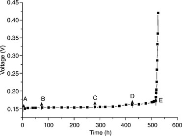
Figure 10.3 shows the typical variation in voltage as a function of time. Solder interconnects experiencing EM mostly exhibit such a characteristic of the variation in resistance.23,28,29 There is a long incubation time with very little resistance change below 90% of the stressing time. The solder joints only contribute to a minor resistance in the whole interconnect structure as compared with the Al traces and the Cu conductors; thus, the effect of void propagation on the resistance of the interconnect structure was less significant before the UBM was completely detached from the solder. This is why solder interconnects mostly retained a low electrical resistance in the early stages of the stressing time, although void accumulation has occurred in the solder joints. After the UBM was completely detached from the solder, the resistance rose abruptly to an open circuit.
10.2.2 Lifetime statistics and the reliability of EM
From an engineering standpoint, a mean-time-to-failure (MTTF) estimation of solder interconnects is of great interest, and a systematic reliability evaluation of EM is needed. For Al interconnects, it is reported that the EM lifetime mostly follows a log–normal distribution. Black’s model was introduced to describe the EM lifetime of a solder based on the assumption that the failure is controlled by void damage, and a log–normal function has been applied frequently.29–31 However, the reason for such a log–normal distribution has not been clarified. However, a Weibull analysis has been performed on time-to-failure (TTF) data in other studies.6,32 In our case, the EM failure of Sn3.5Ag1.0Cu solder joints followed Weibull statistics closely, with current densities ranging from 1 × 10⁴ to 2 × 10⁴ A cm−2 at 100, 125, and 150 °C.14 Figure 10.4 illustrates the distribution function under various current densities at 125 °C. As expected, the reliability of EM degraded with an increase of current density.
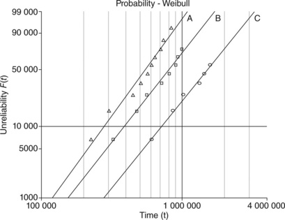
10.4 Weibull cumulative distribution under various current densities at 125 °C (A: 2.0 × 10⁴ A cm−2; B: 1.5 × 10⁴ A cm−2; and C: 1.0 × 10⁻⁴ A cm−2).14
Nevertheless, the predicted lifetimes did not match well with the measured ones, particularly under a higher current density.33 As a result, this study suggests that the model should be modified to include the effect of current crowding and Joule heating. A modified Black’s equation was proposed by inserting a multiplying factor (c) of the current density and a temperature increment (ΔT) into Black’s equation:33,34
where A is a constant, j is the current density in the solder, m is an exponent for current density, Q is the activation energy for EM, k is Boltzmann’s constant, and T is the average temperature.
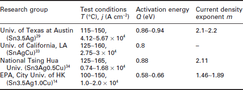
By adding the current factor and a constant temperature increment, Choi et al. obtained activation energies of 0.5 and 0.8 eV for SnPb and SnAgCu solders, respectively.33 Chae et al. also considered the effect of Joule heating: the activation energy calculated was 0.86~0.94 eV and the current density exponent was 2.1~2.2 for SnAg solder joints.29 In addition, by virtue of a numerical simulation and temperature coefficient resistance method (TCR = ΔR/R0ΔT, R0 is the resistance of the Al trace at T0, ΔR is the resistance variation, and ΔT is the temperature rise), we deduced the c and the ΔT (depending on the applied current and ambient temperature), respectively. The average activation energy obtained was about 0.62 eV, and the current density exponent ranged from 1.46 to 1.89.14 Table 10.2 presents the EM reliability parameters for Sn-based lead-free solder interconnects from accelerated life tests in different studies.14,29,33,34
More recently, Chiang et al. compared the predicted values based on Black’s equation, with the predicted values based on the modified equation, and the measured MTTFs under test conditions of different current densities and temperatures. They found that the deviation of predicted values from the experimental results were reduced based on the modified equation.34 Indeed, further effort is necessary to identify the actual current density and bump temperature in solder interconnects. Also, the physics of failure after accelerated life tests needs to be established to confirm its consistency with the proposed failure mechanism. Otherwise, the EM reliability would be incorrectly evaluated.
10.3 Joule heating-enhanced dissolution of under bump metallurgy (UBM) and the diffusion of on-chip metal interconnects
10.3.1 Effect of Joule heating owing to current stressing
In high-current density packages, heat accumulation cannot be ignored because Joule heating is proportional to the square of the current density. The current-crowding effect inevitably leads to a local temperature rise, which in turn accelerates the nucleation and growth of voids inside the solder joint. More significantly, as the foremost heat source, Joule heating from the on-chip metal interconnects is of particular concern. This was verified with thermal infrared measurements.35 Figure 10.5 shows the temperature distribution in a flip-chip interconnect when stressed by 104 A cm−2 at an ambient temperature of 70 °C. The temperature in the middle of the Al traces was much higher than that at the circular Al pads. The edges of the UBM (marked point A) and the passivation openings (marked point B) also exhibited higher temperatures than the Al pads above the solder joints. Numerical simulation of the temperature distribution within solder interconnects supported the infrared measurement.35–37
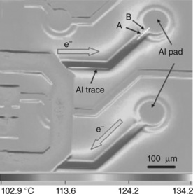
10.5 Thermal infrared measurement for the chip side, with the Al trace exhibiting the highest temperature.35
Since the Al trace is the dominant heat source together with local Joule heating inside of the solder, it is expected that hot spots should occur where the Al traces enter the solder joint. Near this hot spot region, atomic diffusion is thermally accelerated so that the UBM layer is damaged. Also, lattice diffusion of Al atoms is possibly initiated because of the local high-current density itself. These mechanisms may be combined and this is discussed later.
10.3.2 Dissolution of UBM layers and possible solutions
The dissolution of a Cu UBM in a eutectic Sn37Pb solder joint under current stressing has been detected.38,39 Under a current density of 103 A cm−2 at 150 °C for 0.5 h, the solder joint failed with an open circuit, as one of the corners of the Cu UBM was dissolved and replaced by solder according to the microstructural analysis. Hu and coworkers also reported the rapid, asymmetrical, and localized dissolution of a Cu UBM at the cathode side.40,41 The average dissolution rate was 1 μm min−1 when the current density through the eutectic Sn37Pb solder joint was 2.5 × 10⁴ A cm−2 at 100 °C. From the location and geometry of the dissolved Cu, the research suggests that current crowding played a critical role in this rapid dissolution. When the current density was increased to 4 × 10⁴ A cm−2, extensive dissolution of the Cu UBM occurred even at an ambient temperature of 30 °C.
The rapid dissolution of Cu UBM is attributed to an interstitial diffusion of noble and near-noble metals enhanced by Joule heating. It is well known that the interstitial diffusion of dilute elements in tin is significant.42–44 A series of fundamental studies on diffusion and EM of Cu, Ni, Ag and Au in lead–tin alloys have been developed since the 1980s.45–47 As the lattice constants of a and b in tin are much larger than that of the c axis, the open structure along the c axis facilitates faster interstitial diffusion than along the other orthogonal directions. Taking Ni for example, the diffusivity of Ni along the tetragonal c axis is about 7 × 10⁴ times than that at right angles at 120 °C,44 and the EM is very fast, relatively.
Therefore, it is not difficult to understand why Ni was consumed during EM experiments also, although Ni is used as a diffusion barrier in UBM application. Figure 10.6 illustrates the effect of EM on a multilayer UBM film of Ti (0.2–0.5 μm)/Ni(V) (0.325 μm)/Cu (0.5–1.0 μm).48 It was found that, after experiencing a downward electron flow, the Ni and Cu constituents in the UBM began to spread into the solder, and the UBM was gradually consumed. In this instance, voids formed at the UBM/intermetallic compound (IMC) interface owing to UBM consumption under the combined effect of interstitial diffusion and large Joule heating.
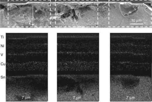
10.6 Elemental mapping at the UBM/IMC interface in a Sn3Ag1.5Cu solder joint after 1967 h under a current density of 1 × 10⁴ A cm−2 at 150 °C.48
It has been proposed that a possible solution to the effects of EM in solder joints would be a thick Cu pillar. The thick Cu pillar could be fabricated as the UBM, and a thin cap layer of solder would be required for the bump, as shown in Fig. 10.7.3 An additional electroplated Ni layer has been suggested to suppress Cu diffusion into the solder body, thus practically inhibiting IMC formation and Kirkendall voiding.49 It is expected that this will be effective in dealing with the problem of UBM dissolution and void accumulation, because the thick Cu pillar is designed to spread the current from the contact to an approximately uniform and low density. This proposal has been supported by experimental studies and numerical simulation.50,51 However, a substantial formation of IMC at the interface is becoming an issue. Also, TM may be initiated because a large temperature gradient is generated across the shallow solder interconnects.
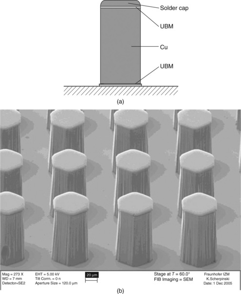
10.7 (a) Schematic diagram of a Cu pillar bump with a solder cap, and (b) focused ion beam (FIB) image of Cu pillar bumps with a height of 80 μm.3
Recent studies have noted that the rotation of β-Sn grains occurred in Sn-based solder under current stressing because of their anisotropic properties.52,53 This re-orientation resulted in a realignment of Sn grains along with the current flow, thereby reducing the resistance of the solder. It is also known that the diffusion of Ni/Cu in UBM was much enhanced along the c axis of Sn crystals, which contributed to the dramatic dissolution of the UBM. Therefore, one should argue that the orientation of Sn grains is closely related to the reliability of Sn-base lead-free solders. Lu et al. investigated the effect of Ag in a Sn-based solder and concluded that the grain re-orientation of Sn was blocked owing to the presence of cyclic twinning and a stable Ag3Sn IMC network; in turn, the dissolution of UBM was comparatively mitigated.54 Lu et al. further explored the effect of an additional 0.6 wt% Zn in Sn1.0Ag solder and obtained a positive result.55 The Zn doping stabilized the Ag3Sn and Cu6Sn5 IMC networks, and suppressed the formation of Cu3Sn IMC. More importantly, polycrystalline-like structures formed at the solder/UBM interface. Although it seems that Zn doping could not control the grain orientation in bulk solder, the strong binding with Cu effectively slowed down the Cu diffusion, and thus stabilized the solder microstructure. Lu et al. present a creative study that explores the doping effect on the microstructural evolution and thus the enhancement of EM resistance. Further nano-doping of solder is also anticipated to support a higher current density and to attenuate the EM damage.
10.3.3 Melting of solder interconnects owing to aluminum diffusion
For flip-chip solder joints with an Al/Ni(V)/Cu UBM, if the Ni layer is consumed completely, the adhesion of the UBM to the solder is degraded. In addition, Al diffusion in the Al trace is triggered as a result of the high current density and local heating. Liu and Lin reported an Al flux-induced failure at the cathode side of an Sn97Pb and Sn37Pb composite solder joint with a downward electron flow.56 Figure 10.8a shows that the location of the Ni layer matched accurately with that of the Cu layer. In the downward electron flow case, the Ni(V) layer would be gradually consumed over a prolonged period of time. As Fig. 10.8b shows, the Ni completely diffused into the solder and the V layer was also damaged. Furthermore, Al started to spread within the solder joint. EM and the accompanying Joule heating drove the Al away from the Al trace and pushed it into the solder. The diffusion of Al into an Sn3.5Ag solder was also detected by Shao et al.57 They found that the solder filled in where a Ti/Cr-Cu/Cu UBM had been located, and CuAl2 IMC formed in the region where the Al pad had been situated.
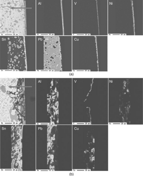
10.8 Elemental mapping of the interface between a solder and the UBM (a) unfailed after 1000 h current stressing, and (b) failed after 1711 h current stressing.56
Using an infrared microscope Liang et al. detected the fracture of an Al trace while the current density through the Al trace was about 1.2 × 10⁶ A cm−2.58 They speculated that EM damage had also occurred in the Al trace, and that the degradation of the Al trace may be responsible for an abrupt temperature rise. Additionally, their thermoelectric simulations supported this. It was the degradation of the Al trace, instead of void formation, that contributed to the formation of a hot spot.
It has been proposed that solder melting under current stressing is a time-dependent phenomenon.59,60 According to previous research, the principal reason for an incubation time was attributed to the process of void generation and propagation, and solder lifetime was explained through modeling void accumulation.24,41 However, Ouyang et al. have observed the melting of eutectic Sn37Pb solder joints owing to the Joule heating of the Al traces.59 They suggested that Al dissolution expedited the rise of a solder interconnect’s electrical resistance and hence led to the final melting of the solder. Because the resistance change of the Al trace was dependent on the dissolution rate of Al into the solder, an incubation period was required for a temperature rise that could provide sufficient heat to melt the solder joint. In this way, Ouyang et al. explained why the melting of the solder exhibited a time-dependent characteristic.
Recently, the melting failure of Sn3.5Ag1.0Cu solder interconnects has been studied under a current density of 2.3 × 10⁴ A cm−2 at 125 °C.61 A new failure mechanism involving the combined effect of solder EM and Al diffusion has been proposed. Figure 10.9 shows typical stages of the morphological evolution. Firstly, with a downward electron flow, voids occurred at the interface between the Cu–Sn IMC layer and the solder, especially in the current crowding region (Fig. 10.9a). Secondly, as Fig. 10.9b shows, the voids gradually extended to the surrounding areas owing to vacancy supersaturation. Thirdly, the creation of pancake-type voids decreased the effective contact area, which led to more serious current crowding. Meanwhile, the Joule heating owing to current crowding was enhanced because of poor heat dissipation around the voids. Under such accumulated effects, the atomic diffusion of Ni(V) in the UBM was accelerated, and the barrier that prevents the dissolution of Al into the solder no longer existed. Therefore, the diffusion of Al was triggered and some voids were found in the Al pad, as demonstrated in Fig. 10.9c. Also, the local magnified micrograph shown in Fig. 10.9f demonstrates that the Ni(V) layer previously attached to the Al pad had disappeared as compared with Fig. 10.9e. Ni atoms were dissolved and consumed to form a Cu–Ni–Sn ternary IMC, and the V layer above the voids extruded and began to lose its structural integrity, so that the dissolution of Al through this layer was more rapid. Fourthly, with the progress of Al dissolution, the dramatic Joule heating may damage the interfacial integrity between the Al trace and the passivation layer, as shown in Fig. 10.9d. More significantly, EM in the connecting Al trace was initiated and expedited, so that further melting failure of solder interconnects was produced.
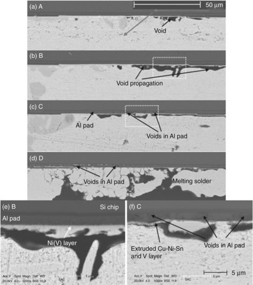
10.9 SEM images of different stages of the morphological evolution in Sn3.5Ag1.0Cu solder joints under a current density of 2.3 × 10⁴ A cm−2 at 125 °C after (a) 92 h, 25% of the failure time, time point A, (b) 245 h, 66%, B, (c) 295 h, 80%, C, (d) 361 h, 98%, D, (e) local magnified micrograph of the interface at time point B, the dotted region in (b), and (f) C, the dotted region in (c).61
A finite element simulation was applied to understand the current density distribution in the flip-chip interconnects. Figure 10.10 displays the evolution of the current density in Al interconnects alone (as viewed from underneath). The current density reached more than 106 A cm−2, which is sufficiently high for triggering the EM of the Al. According to Fig. 10.10a, the current density at the exit location of the Al pad ranged from 1.2 × 10¹⁰ to 1.4 × 10¹⁰ A m−2 (i.e., from 1.2 × 10⁶ to 1.4 × 10⁶ A cm−2) before voids were developed. The modeled maximum value occurred at the connecting corner of the Al pad and the Al trace. By contrast, when the voids propagated, the location of the maximum current density was transferred to the exit location of the Al pad, and it reached 1.7 × 10¹⁰ A m−2 (i.e., 1.7 × 10⁶ A cm−2), as shown in Fig. 10.10b. This simulation indicates that the current density through the Al pad was enhanced owing to the decrease of contacting area at the interface, and this result supports the experiments.
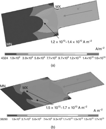
10.10 Current density distribution in the Al interconnect alone (as viewed from underneath): (a) before void growth (current density at the exit location was 1.2 × 10¹⁰~ 1.4 × 10¹⁰ A m−2), and (b) after void growth (current density at the exit location was 1.5 × 10¹⁰~ 1.7 × 10¹⁰ A m−2).14
The total incubation time for melting the solder was dependent on the rates of void growth and Al diffusion in this instance. Therefore, the solder melting exhibited a unique time-dependent characteristic. In the initial stages, the rate of void growth varied from 0.24 to 0.53 μm h−1. This rate was related to the void nucleation and propagation. In the later stage, before the final failure, the depletion of the Al also exhibited a linear relationship with time, which was ascribed to the EM of the Al interconnect.
It has been known that the change in trace resistance is a linear function of the atomic drift velocity.62 In this case, the relationship between the rates of trace resistance change (∂(ΔR/R)/∂t) and material depletion (∂(ΔL)/∂t) may be described as:
where the subscripts r and Al refer to the under-layer and Al trace, respectively, ρ is the electrical resistivity, S is the cross-sectional area of the specific layer, R is the initial trace resistance, L is the initial trace length, and vd is the atomic drift velocity. Based on an electrical characteristic, the rate of resistance change was estimated to be 0.9% h−1. This rate of change then represents the drift of Al atoms in the later stage.
10.4 Stress-related degradation of solder interconnects under EM
10.4.1 Morphological evolution owing to EM and a back stress in solder interconnects
When atoms are driven from the cathode to the anode by the electron wind force, the latter are in compression and the former in tension. In a cross-sectioned solder joint for an in situ observation, it is expected that the compressive stress is released from the free surface, causing hillocks or whiskers to occur at the anode. Using thin film solder strips, Liu et al. first investigated the formation of atomic hillocks in pure tin under a current density of 105 A cm−2 at room temperature.12 An explanation was given in terms of a stress relief mechanism that a hillock or whisker grows from the surface under compression.63
Synchrotron X-ray microscopy has been applied to provide information regarding a depth profile for the accumulated stresses.64,65 Figure 10.11 demonstrates the hillock and valley formation in a eutectic tin–lead solder joint under a current density of 104 A cm−2 after 72 h. The depth profile obtained with confocal laser microscopy for the joint, which is shown next to the micrograph, indicates that the maximum height of the hillocks near the anode was about 16 μm, and the depth of the valley near the cathode was about 34 μm. It can also be seen that the surface features of the hillock region exhibited rows of striations with a spacing of several micrometers. These striations were on the side of the hillock facing the anode, and initiated from the anode end then propagated in the direction opposite to the electron flow during current stressing. Such markings can be considered as an indication of the material forced out as a result of the compressive stress.
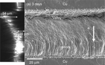
10.11 Hillock and valley formation in a eutectic tin–lead solder joint under a current density of 104 A cm−2 after 72 h (The depth profile is shown to the left).65
Ouyang et al. reported the formation of whiskers in solder joints.66 Figure 10.12a and 10.12b show the growth of whiskers at the upper right corner (anode side) in eutectic SnPb and SnAgCu solder joints under a current density of above 104 A cm−2 after 48 h and 248.5 h, respectively. The composition of the whiskers was confirmed as 93 wt% Sn by EDX. These whiskers initiated from the cracked surface at the chip side. When Pb atoms were pushed towards the anode, a compressive stress on Sn-rich grains was produced and then Sn whiskers were forced out. Moreover, it was noticed that the cross-sectioned surface of the SnPb solder exhibited a dimple and bulge structure after EM, whereas the surface of SnAgCu solder remained flat. This phenomenon suggests that the rate of EM in SnAgCu was smaller than that in SnPb.
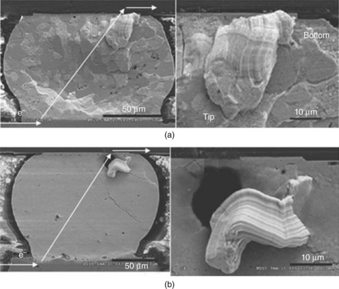
10.12 Whisker growth at the anode (chip side) (a) a eutectic SnPb solder joint under a current density of 104 A cm−2 after 48 h, and (b) SnAgCu solder joint under a current density of 1.4 × 10⁴ A cm−2 after 248.5 h.66
On the basis of the Nabarro–Herring model of the equilibrium vacancy concentration, more vacancies are generated in the tensile region, whereas fewer vacancies occur in the compressive region; therefore, the vacancy concentration gradient decreases from the cathode to the anode.67 The atomic flux under a combined electrical and mechanical force can be expressed as:
where σ is the hydrostatic stress, dσ/dx is the stress gradient, and Ω is the atomic volume. The other terms have been defined before. The first part represents the flux owing to EM, whereas the second part stands for the opposite flux owing to back stress.
A plausible explanation for the above difference between the rates of EM of SnAgCu and SnPb is then given in terms of the back stress.66 Because the elastic modulus or stiffness of the SnAgCu solder is larger than that of the SnPb, the back stress gradient in SnAgCu could be higher. Hence, the effect of the back stress on the retardation of EM was relatively larger for the SnAgCu solder.
If stress balances with wind force at a critical length, there should be no net atomic flux (J = 0), which has been well known as the Blech condition.68 According to equation [10.5], the critical length (Xc) can be obtained:
The effect of back stress and the critical length in a solder was investigated by Wei and Chen.69 In Wei and Chen’s study, eutectic SnPb solder strips with lengths ranging from 5 to 200 μm were prepared and a length-dependent EM behavior was identified. Figure 10.13 shows the microstructural characteristics of various solder strips under a current density of 2 × 10⁴ A cm−2 after 490 h at 100 °C. No material depletion or voids could be detected for the 5 and 10 μm long strips. By taking the critical compressive yield stress (σc) of SnPb solder (27 MPa), the critical length was estimated to be 11 μm under such experimental conditions. This value agrees with the experimental results.
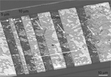
10.13 Microstructural characteristics of various solder strips under a current density of 2 × 10⁴ A cm−2 after 490 h at 100 °C (no material depletion could be detected for the 5 and 10 μm long strips).69
The effect of the back stress was further studied by an area array of nanoindentation markers on the cross-section of solder joints by Xu et al.70 Most markers moved against the EM-induced atomic flux, indicating that in this instance the effect of the electron wind force was larger than that of the back stress. After 360 h of current stressing, the average marker movement from the cathode to the anode was plotted, as shown in Fig. 10.14a.
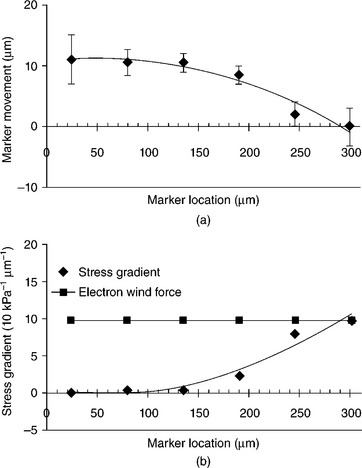
10.14 (a) Marker movement at different locations in a solder joint under current stressing after 360 h, and (b) the stress gradient as a function of the location.70
Also, the atomic flux can be calculated as follows:
where V is the total volume of atomic transport, u is the marker displacement, Ω is the atomic volume, S is the cross-sectional area, and t is the operation time.
By combining equations [10.5] and [10.7], and assuming that the effect of the back stress gradient on the marker movement could be neglected when the marker was far enough from the anode, the stress gradient as a function of the marker displacement. When defining K = (1/C)(kt/D)(1/Ω2t) can be described as:
where uo is the marker displacement near the cathode, and K is a constant for a given temperature and time.
Hence, the stress at any location is:
Substituting u(x) and the boundary conditions into equation [10.9], the stress gradient at any location could be determined, as shown in Fig. 10.14b. The stress gradient near the anode was 97 kPa μm−1, and it decreased gradually to zero with distance.
10.4.2 Mechanical deformation and degradation under current stressing
To detect the EM-induced mechanical damage, a Moiré interferometric technique was used to obtain the in situ displacement evolution of solder joints under electric current stressing.71 Large deformations may be observed in solder joints under a current density of 104 A cm−2. Figures 10.15a and 10.16a display the U field and V field fringes in an Sn4Ag0.5Cu solder joint after 1500 h of current stressing, respectively. The U field fringes were predominantly in the vertical direction with concentrations on both vertical edges, indicating that a large normal deformation was developed in the horizontal direction. Instead, the V field fringes were predominantly in the horizontal direction, suggesting a large normal deformation in the vertical direction. In addition, Fig. 10.15b and Fig. 10.16b show the field fringes after the current was switched off. Although the fringes became less clear, there were little changes in both U and V field fringes. This means that the deformations created by the high current density were irreversible, which is attributed to both the re-arrangement of defects and atoms in the material and also the accompanying local volumetric change.
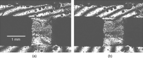
10.15 U field fringe of an Sn4Ag0.5Cu solder joint (a) during current stressing, and (b) after the current was terminated.71
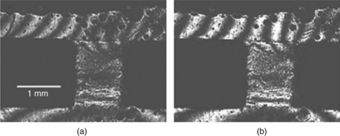
10.16 V field fringe of an Sn4Ag0.5Cu solder joint (a) during current stressing, and (b) after the current was terminated.71
Nano-indentation tests were conducted to explore the mechanical behavior of solder joints after EM.14 Figure 10.17 illustrates the modulus variation of Sn3.5Ag1.0Cu solder joints under a current density of 2.0 × 10⁴ A cm−2 after various stressing times at 125 °C. It is apparent that the modulus of solder joints decreased after current stressing, and the mechanical properties were degraded compared with the original values. Therefore, when interfacial voids are initiated owing to flux divergence under EM, bond damage occurs in solder joints. From a physical perspective, the modulus is directly related to the atomic bonds. Hence, it is understandable that the modulus decreased with the passage of time under current stressing.
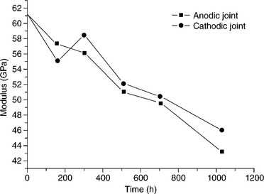
10.17 Variation of modulus of Sn3.5Ag1.0Cu solder joints under a current density of 2.0 × 10⁴ A cm−2 after various times at 125 °C.14
The effect of EM on the shear behavior of flip-chip solder joints was studied by Nah et al.72 It was found that the mode of shear failure changed after EM and depended on the direction of electron flow. Originally, shear-induced fracture occurred in the bulk of the solder without current stressing. However, as shown in Fig. 10.18, under a current density of 2.55 × 10⁴ A cm−2 after 10 h at 140 °C, fracture occurred instead at the cathode interfaces between the solder and IMCs. This is because EM dissolved and drove Cu or Ni atoms from the UBM or bond pad into the solder, resulting in the large growth of brittle Sn-based IMCs at the cathode side. Therefore, shear failure occurred predominantly at the cathode interface.
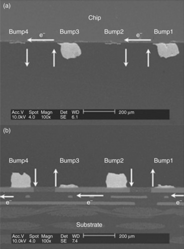
10.18 SEM images of solder joints after mechanical shear testing under a current density of 2.55 × 10⁴ A cm−2 after 10 h at 140 °C (a) chip side, and (b) substrate side.72
Also, fractographs of solder joints before and after EM were examined for a comparison.18 Figure 10.19 shows the typical sheared fracture surfaces of Sn3.5Ag1.0Cu solder joints (substrate side) under a current density of 2.1 × 10⁴ A cm−2 at room temperature. During the test without current stressing, the fracture mode was in the bulk solder cutting through the region just near the (Cu,Ni)6Sn5 IMC layer, and the fracture surface exhibited great amounts of ductile deformation with large dimples. At longer stressing times, the interface became brittle and a smaller amount of plastic deformation was observed. This mechanical deterioration with changes in stressing time is attributed to void formation and stress accumulation at the interface.
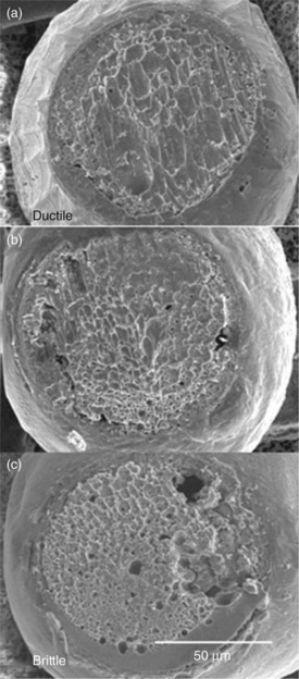
10.19 Typical fractographs of Sn3.5Ag1.0Cu solder joints (substrate side) (a) as reflowed, (b) under current stressing after 144 h, and (c) under current stressing after 288 h.18
10.5 Thermomigration (TM) behavior in solder interconnects under a thermal gradient
With the trend towards greater integration and further miniaturization in the microelectronics industry, the cross-sectional area of conductive lines on chips has been decreased significantly. This decrease has led to a dramatic accumulation of Joule heating in first-level interconnects, as discussed in 10.3.1. Then a considerable thermal gradient could build up across solder joints, thus providing a driving force for atomic diffusion to trigger TM.
10.5.1 TM in tin–lead solder interconnects
The earliest report regarding the combined effects of EM and TM in solder joints was given by Ye et al.73 With microstructural observations and marker measurements, Ye et al. found that TM in flip-chip solder joints may assist or counter EM, depending on the direction of the thermal gradient and electric field.
The individual contribution of TM to the failure of solder joints was described by Huang et al.74 They proposed the design of a test structure of flip-chip solder joints that can be applied to conduct TM without EM. Generally, in the interconnect structure, the Al traces are the primary heat sources because of their large resistance. Hence, it is believed that a certain thermal gradient exists in the powered solder joints as a result of the temperature difference. Moreover, owing to the excellent thermal conductivity of the silicon chip, a similar thermal gradient is also formed across the adjacent unpowered solder joints. These unpowered solder joints are thus investigated for a TM study since no current is applied to them.
Morphological evolution owing to TM has also been detected in eutectic tin–lead solder joints. Figure 10.20a shows SEM images of a row of tin–lead solder joints after 50 h at 150 °C. Figure 10.20b demonstrates the detailed microstructure of joint 4 at a higher magnification.75 According to these micrographs, it is believed that Pb migrated to the substrate side under the temperature gradient across the unpowered solder joints. This was supported by the EDX analysis of local regions. As shown in Fig. 10.20b, the average concentration of accumulated Pb at the substrate side was about 65.2 at%, and the concentration of Sn at the chip side approached 86.3 at%. The width of the accumulated Pb-rich phase band reached approximately 15 μm, i.e., half of the joint standing height. This result agrees with TM in tin–lead composite flip-chip solder joints.74
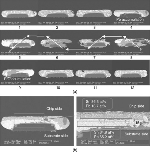
10.20 (a) SEM images of a row of solder joints from 1 to 12, with solder joints from 5 to 8 under current stressing after 50 h at 150 °C (Pb accumulation in the unpowered solder joints 4 and 9), and (b) the detailed microstructure of joint 4 at a higher magnification.75
A possible explanation for the above microstructural evolution is as follows. The flow of atoms under a thermal gradient depends on the heat of transport (Q*), defined as the difference between the heat carried by the moving atoms and the heat of the atoms in the initial state (the hot end or the cold end).76 For the atoms which move from the hot end to the cold end, the Q* is negative because they lose heat. For atoms moving from the cold to the hot end, the Q* is positive. Pb atoms are the dominant diffusing species with a higher diffusivity in eutectic tin–lead solder above 120 °C77,78 Therefore, based on the microstructural evolution as shown in Fig. 10.20, it is speculated that with a negative Q*, Pb atoms migrated from the higher temperature side to the lower temperature side under the temperature gradient. Meanwhile, Sn atoms moved slowly and replenished the vacancies owing to the depletion of Pb atoms. Macroscopically, the Pb-rich phase migrated to one side and the Sn-rich phase was ‘pushed’ towards the opposite side on the basis of a constant volume process. However, the mechanism of the reversed Sn flux during TM remains unclear, and the sign of Q* for Sn cannot be confirmed as yet.
It is important to obtain the temperature distribution of first-level solder interconnects to understand the TM behavior of solder joints. Finite-element modeling and simulation were applied to predict the electrothermal characteristics, and the result showed that a temperature gradient greater than 1000 °C cm−1 built up across the unpowered joint owing to the Joule heating from the neighboring Al traces.75 A simulation by Ye et al. also showed the existence of a thermal gradient of about 1500 °C cm−1 in flip-chip test structures.73 In combination with the simulation, thermocouples and the temperature coefficient of resistance method were used to verify real temperatures in solder interconnects.79 However, because of the unique interconnect structure and the limitation of these measurement methods, it is difficult to pinpoint the temperature gradient across solder joints. Recently, a thermal infrared technique was employed by Hsiao and Chen to obtain the thermal gradient directly in cross-sectioned solder joints.80 As can be seen from Fig. 10.21a, a uniform temperature distribution occurred in the solder bump before current stressing. Then Fig. 10.21b shows the temperature distribution of a solder joint under an alternating current density of 9.2 × 10⁴ A cm−2. Because there is no EM effect under alternating current stressing, and the alternating current produces a similar Joule heating as the direct current does, the alternating current was applied to independently investigate the TM behavior in solder joints. Figure 10.21c shows the temperature profile along the dashed line in Fig. 10.21b, in which the average temperature at the chip side was 16.0 °C higher than that at the substrate side. The thermal gradient was calculated to be approximately 2143 °C cm−1. This trial is significant since it verified the existence of a large thermal gradient across real flip-chip solder joints with experimental data.
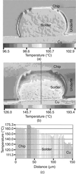
10.21 (a) Temperature distribution of a solder joint before current stressing, (b) under an alternating current density of 9.2 × 10⁴ A cm−2, and (c) the temperature profile along the dashed line in (b) (the thermal gradient was estimated to be 2143 °C cm−1).80
In addition, from Fig. 10.20b it is noticeable that the Pb-rich phase accumulated at the lower left side, i.e., the lower-temperature region of solder joint 4. Likewise, the Pb redistribution in solder joint 9 showed a similar tendency, i.e., Pb migrated to the lower right side (the lower temperature region), as Fig. 10.20a shows. As an example, because the right side of solder joint 4 was closer to the heat source, it is possible that a temperature gradient was established laterally from the right side to the left side. Thus the Pb-rich phase not only migrated to the substrate side under the vertical temperature gradient, but also moved to the lower temperature region driven by the lateral temperature gradient across this solder joint. This lateral TM was also observed in composite solder joints.74,81
Morphological variations at different cross-sectional planes of a solder joint during TM are involved because of differing thermal dissipations.79 Figure 10.22a shows the obvious TM of Pb at the periphery of two solder joints, which is similar to that of Fig. 10.20. Then a stepwise cross-sectional analysis was conducted by gradually grinding the solder joints to the center of the passivation opening. Figure 10.22b demonstrates the cross-sections of solder joints 4 and 9 after re-polishing approximately 50 μm. It is noted that the TM of Pb was not as apparent as that in Fig. 22a. Pb-rich phases were uniformly distributed in solder joint 4. Pb accumulation in solder joint 9 was also slight and only the Pb-rich phase at the periphery of the solder exhibited a TM characteristic. Therefore, the TM of the inner solder region was less significant than that of the outer solder (the surface layer). One can understand that the temperature distribution inside the center of a solder joint became more uniform. By contrast, it is easier for a large thermal gradient to build up across the surface layer of solder joints where a substantial heat dissipation is achieved, because the outer solder is close to the ambient environment.
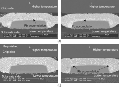
10.22 SEM images of two cross-sectional planes for unpowered solder joints 4 and 9 (a) after the first polishing (outer solder), and (b) after repolishing approximately 50 μm (inner solder).79
It is worth mentioning that during the TM, the Pb grains were even more uniformly dispersed in the tin matrix, although the bulk of the Pb had moved to the substrate side, as shown in Fig. 10.20b. This means that the lamellar microstructure became much finer after the TM process. This microstructure change has also been detected in Sn58Bi solder joints under a TM-enhanced effect in our group.82 Ouyang et al. found a similar phenomenon.83 They suggested that the formation of this finer lamellar structure created a more disordered higher entropy state.2,83 Also, according to their estimate, entropy production by heat propagation was many orders of magnitude larger than that by atomic migration, and it is thus conceivable that entropy production in TM could affect the microstructure substantially.
In order to understand the mechanism of atomic transport, the atomic flux and the heat of transport during the TM process were estimated. Taking a central displacement (Δx) of 7.5 μm in Fig. 10.20b, the total volume of atomic transport (Vtm) during the operation time (t) can be approximately obtained from the product of the displacement and the cross-sectional area (S) of the solder joint. Therefore, taking the atomic volume of Pb (Ω) as 3.0 × 10⁻²³ cm3, the atomic flux of Pb owing to TM (Jtm) can be calculated as follows:
In addition, the atomic flux owing to TM can be expressed as equation [10.2] as shown in 10.1.2. Hence, taking a predicted temperature gradient of 1100 °C cm−1, an atomic diffusivity of Pb of 4.0 × 10⁻¹³ cm2 s−1,78 we substituted these values into equation [10.2], and obtained the molar heat of transport as approximately − 27.2 kJ mol−1. Compared with the result reported by Ouyang et al. (− 25.3 kJ mol−1),83 the molar heat of transport of Pb is slightly different.
In addition, Chuang and Liu estimated the molar heat of transport of Pb as − 22.2 kJ mol−1 under a thermal gradient of 1010 °C cm−1, by measuring the displacement of artificial markers.84 Significantly, they found that the average displacement of atoms increased almost linearly with time during TM. More recently, markers fabricated by a focused ion beam (FIB) method were used to measure the rate of TM by Hsiao and Chen.80 With a thermal gradient of 2143 °C cm−1, a molar heat of transport of − 26.8 kJ mol−1 has been obtained for the transport of Pb.
10.5.2 TM in tin-based lead-free solder interconnects
As stated above, the migration of the Sn flux during TM is unclear and this has necessitated further investigations for lead-free solders. A more recent study by Hsiao and Chen further reveals the TM characteristic of Sn in lead-free solder.85 They investigated the TM behavior of Sn in Sn3.5Ag solder joints under a temperature gradient of 2829 °C cm−1 at 100 °C. As mentioned in 10.5.1, an alternating current was used to eliminate the EM effect, thus facilitating an independent study of TM. After 800 h of TM testing with a 0.57 A alternating current, it is significant that hillocks were pushed out from the chip side, as shown in Fig. 10.23b. These hillocks were generated by the mass transfer of the Sn at the hot side, providing direct evidence that Sn was transported along the direction opposite to the thermal gradient. In addition, by measuring the marker movement, they obtained the TM flux and molar heat of transport of Sn as 5.0 × 10¹² atoms cm−2 s−1 and 1.36 kJ mol−1, respectively, which are smaller than those of Pb atoms listed in 10.5.1. Our studies also show the similar tendency of Sn atoms migrating towards the higher temperature side in Sn3.0Ag0.5Cu solder joints under a thermal gradient.14,86
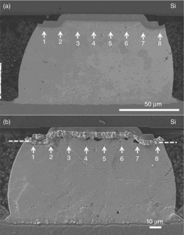
10.23 (a) Original micrograph of a Sn3.5Ag solder joint and (b) micrograph of a solder joint after 800 h of TM testing with a temperature gradient of 2829 °C cm−1 at 100 °C. (Note that the Sn whiskers were present at the chip side, and the markers moved toward the substrate side.)85
Microstructural evolution in Cu/Sn4Ag0.5Cu/Cu solder interconnects has been studied under a thermal gradient of 1000~1200 °C cm−1, and a TM of Cu atoms has been proposed.87,88 It has been found that the two major microstructural differences between TM and isothermal samples were the lack of a Cu3Sn layer at both the higher and lower temperature sides, and the thinning of the Cu6Sn5 layer at the higher temperature side for the TM samples. Supposedly, this thinning of the Cu6Sn5 layer occurred because of its disintegration, during which the Cu atoms moved to the lower temperature side under the thermal gradient. Meanwhile, the absence of the Cu3Sn layer was a result of an insufficient Cu concentration. More recently, the TM of interstitial Cu in SnAg flip-chip solder joints was reported by Chen et al.89 Chen et al. suggested that the void formation at the chip side was attributed to a fast interstitial diffusion of Cu atoms from the UBM into the Sn matrix. The driving force of Cu diffusion was the result of a large thermal gradient accredited to Joule heating across the solder bumps. Further attempts need to be made to verify the real characteristic of the TM of Cu.
More than that, a specific line-type test structure (Ni/Sn58Bi/Cu) has been applied to investigate the combined effect of EM and TM of Bi, as shown in Fig. 10.24a.82 As Ni shows a higher electrical resistivity than Cu, a large temperature difference may be created at two sides of the solder joint during the current stressing (downward from the Ni to the Cu side). Finite-element simulation has shown that a thermal gradient of about 527 °C cm−1 existed in the solder joint under a current density of 5 × 10³ A cm−2 at 50 °C, as demonstrated by Fig. 10.24b and 10.24c. Temperature measurements using thermocouples also supported this thermal gradient. By varying the direction of the electrical current, the counteracted and enhanced effects of TM were detected separately. It can be seen from Fig. 10.25 that the migration of Bi atoms was more pronounced when the Ni wire was used as the cathode. According to the experimental findings, we speculate that the Bi has a similar TM characteristic to Pb and shows a negative Q*. Then, if the direction of the thermal gradient was opposite to that of the electron flow, the TM counteracted the EM and retarded the diffusion of the Bi atoms (case 1). Otherwise, the TM assisted the EM, and the diffusion of the Bi atoms was enhanced (case 2). In addition, based on the results from these two cases, the atomic fluxes of Bi owing to EM and TM were differentiated and estimated to be 1.48 × 10¹³ atoms cm−2 s−1 and 5.38 × 10¹² atoms cm−2 s−1, respectively.
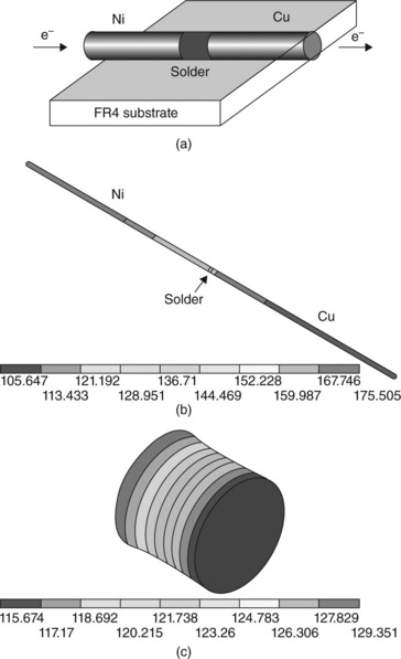
10.24 (a) Schematic diagram of a line-type test structure (Ni/Sn58Bi/Cu), (b) temperature distribution in the test structure, and (c) temperature distribution in the solder joint only (a thermal gradient of about 527 °C cm−1 existed across the solder joint).82
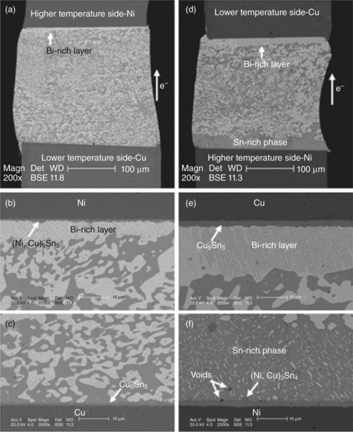
10.25 SEM images of Ni/Sn58Bi/Cu solder joints under a current density of 5 × 10³ A cm−2 after 384 h at 50 °C (a) case 1: EM counteracted by TM, (b) anode side in case 1, (c) cathode side in case 1, (d) case 2: EM enhanced by TM, (e) anode side in case 2, and (f) cathode side in case 2.82
10.6 Conclusions
10.6.1 Summary
In this review, we have discussed four types of physical failure mechanisms of solder interconnects for high current density applications. Interfacial void growth, the essential physical process occurring in EM, was introduced in 10.2. EM reliability parameters for Sn-based lead-free solder interconnects in recent publications were also collected for summary. The modification of Black’s model, which greatly affects the lifetime statistics and reliability evaluation for EM failure, is significant.
Joule heating in first-level solder interconnects is substantial. This was demonstrated in 10.3 through experimental and numerical investigations. Owing to interstitial diffusion enhanced by Joule heating, the consumption of the UBM layer is noticeable so that new structural design (e.g., Cu/Ni pillar) and microstructural improvement need to be developed to support high current densities and to minimize EM. In addition, the Al diffusion-induced damage in flip-chip interconnects has attracted some interest in current research. We have proposed a failure mechanism involving the combined effect of solder EM and Al diffusion, and thus offered an explanation for the time-dependent behavior of solder melting failure under current stressing.
We reviewed the stress-related degradation of solder interconnects under a current density in 10.4. Owing to the relief of compressive stresses, morphological evolution is apparent in the form of hillocks or whiskers near the anode. One important factor, the back stress generated, was investigated to understand the damage caused by EM. In addition, the mechanical deformation was identified through an interferometric technique. In addition, the deterioration of solder interconnects under current stressing was detected through a series of mechanical tests.
An attempt to explore the TM behavior of solder interconnects has been made recently, and this was discussed in 10.5. By employing a testing method of differentiating TM from EM, the TM behavior of Pb was understood in terms of morphological evolution, atomic transport and by numerical simulation. Pb shows a negative heat of transport. The TM of Sn has also been studied. On the basis of experimental findings it is speculated that Sn atoms exhibit a different TM characteristic opposite to that of Pb atoms. More recently, the TM of interstitial Cu has been reported, which states that the Cu also has a negative heat of transport. In addition, a specific line-type test structure has been utilized to investigate the combined effect of EM and TM of Bi. It was revealed that Bi has a similar TM behavior to that of Pb.
10.6.2 Future trends
The current carrying capability of Al/UBM/solder should be considered based on the limitation owing to EM in the design rules. Routing design of Al interconnects needs to be implemented to mitigate the current crowding and Joule heating. A pad structure that produces a uniform current distribution within the bump interconnect is recommended to avoid the dissolution of Al. In occurrences of EM problems with Al, a relative enlargement of the cross-section of the Al trace is also a factor that could be considered. For UBM, in 10.3.2, the solution of a thick Cu pillar with a Ni electroplated layer has been suggested, which can be expected to alleviate the effect of current crowding and of accompanying heat accumulation at the interface. Our research suggests that new solder technologies with improved current density capabilities and a higher operating temperature will be developed in the near future. Considering the Sn-grain rotation under current stressing, a further nano-doping into solder is anticipated to stabilize the microstructure for limiting the fast interstitial diffusion of noble or near-noble metals. In addition, taking into account different applications in industry, EM studies in Sn-based solders should be extended to other lead-free solders, such as InAu.
Although void formation at the UBM side has been confirmed as a major failure mechanism in solder interconnects for high current density applications, IMC growth at the interface cannot be ignored. The extensive IMC growth at the substrate side exerts a great influence on the mechanical reliability. The kinetics dominating interfacial reactions have not yet been established, and the laws of IMC growth (parabolic or linear) under current stressing are still under investigation. Therefore, the interfacial reactions under current stressing are important and challenging problems, particularly for the application of micro-bumps with Cu pillars in 3D packages, such as through silicon via (TSV) bonding, where the IMCs substantially form at the interface; hence, a major phase transformation is induced.90,91
Another issue of key importance is the TM of Sn. Although a small number of recent studies exist, the present understanding of the TM behavior of Sn is still limited. To differentiate TM from EM further, it is suggested that each end of the connecting wires (same materials) in a line-type test structure should be set at different temperatures.92 In this way, the effect of current stressing is completely removed and only the driving force owing to TM is available. As compared with flip-chip samples, the advantages of line-type samples are that the temperature gradient can be measured more easily.
So far, few studies on the combined effect of TM and mechanical stress have been reported.93 For the mechanical characteristics, high strain rate fracture failure is as important as low cycle fatigue failure, which has been of major concern in recent years. Shear tests and tensile tests should be performed to evaluate the mechanical behavior of solder joints after TM. If atoms migrate from the higher to the lower temperature side by the force caused by the thermal gradient, a reversed flux of vacancies moves to the higher temperature side. Consequently, the interface at the higher temperature side becomes mechanically degraded. Therefore, this interaction between TM and the applied stress is of considerable importance.
10.7 Acknowledgements
This chapter contains some material reprinted from Y.C. Chan and D. Yang, Progress in Materials Science, ‘Failure mechanisms of solder interconnects under current stressing in advanced electronic packages’, 55, 428–475 (2010), with permission from Elsevier. We would like to acknowledge the significant contributions from Dr M.O. Alam, Dr B.Y. Wu and Dr X. Gu at the EPA Centre, City University of Hong Kong. Special thanks are extended to Professor B. Ralph at Brunel University, UK, and Dr J. Shen at the EPA Centre, CityU, HK, for their valuable suggestions. We also wish to express our sincere gratitude to Professor K.N. Tu’s group at University of California at Los Angeles (Dr J.W. Nah, Dr F.Y. Ouyang), Professor C. Basaran’s group at State University of New York at Buffalo (Dr H. Ye), Prof. C. Chen’s group at National Chiao Tung University (Dr S.H. Chiu, Dr C.C. Wei, Dr H.Y. Hsiao), Professor A. Lee at Michigan State University, Professor M.H. Ren at National Sun Yat-sen University, Dr K.L. Lin’s group at National Cheng Kung University (Dr Y.H. Liu), Dr L.H. Xu at Intel, Chandler, AZ, for the permission in using their figures to develop discussions.
10.8 References
1. ITRs, International technology roadmap for semiconductorsAssembly and packaging section. San Jose: Semiconductor Industry Association, 2003.
2. Tu, K.N. Solder joint technology: materials, properties, and reliability, 1st. New York: Springer Science + Business Media LLC; 2007.
3. Assembly and packaging sectionInternational technology roadmap for semiconductors. San Jose: Semiconductor Industry Association, 2007.
4. Chen, C., Liang, S.W. Electromigration issues in lead-free solder joints. J Mater Sci: Mater Electron. 2007; 18:259–268.
5. Huntington, H.B., Grone, A.R. Current-induced marker motion in gold wires. J Phys Chem Solids. 1961; 20:76–87.
6. Brandenburg, S., Yeh, S. Proceedings of the Surface Mount International Conference and Exhibition. In: Electromigration studies of flip chip bump solder joints. San Jose, CA: SMI; 1998:337–344.
7. Assembly and packaging sectionInternational technology roadmap for semiconductors. San Jose: Semiconductor Industry Association, 2002.
8. Ye, H., Basaran, C., Hopkins, D.C. Mechanical degradation of microelectronics solder joints under current stressing. Int J Solids Struct. 2003; 40(26):7269–7284.
9. Campbell, D.R., Huntington, H.B. Thermomigration and electromigration in zirconium. Phys Rev. 1969; 179(3):601–612.
10. Yoon, M.S., Lee, S.B., Kim, O.H., Park, Y.B., Joo, Y.C. Relationship between edge drift and atomic migration during electromigration of eutectic SnPb lines. J Appl Phys. 2006; 100:033715.
11. Agarwal, R., Ou, S.Q., Tu, K.N. Electromigration and critical product in eutectic SnPb solder lines at 100 °C. J Appl Phys. 2006; 100:024909.
12. Liu, C.Y., Chen, C., Tu, K.N. Electromigration in Sn–Pb solder strips as a function of alloy composition. J Appl Phys. 2000; 88:5703–5709.
13. Ho, C.E., Lee, A., Subramanian, K.N., Liu, W. Early stage of material movements in eutectic SnPb solder joint undergoing current stressing at 150 °C. Appl Phys Lett. 2007; 91:021906.
14. Yang, D. Study on reliability of flip chip solder interconnects for high current density packaging. Hong Kong: City University of Hong Kong; 2008. [PhD thesis].
15. Gu, X., Chan, Y.C. Electromigration in line-type Cu/Sn-Bi/Cu solder joints. J Electron Mater. 2008; 37(11):1721–1726.
16. Lee, T.Y., Tu, K.N., Frear, D.R. Electromigration of eutectic SnPb and SnAg3.8Cu0.7 flip chip solder bumps and under-bump metallization. J Appl Phys. 2001; 90(9):4502–4508.
17. Wu, B.Y., Alam, M.O., Chan, Y.C., Zhong, H.W. Joule heating enhanced phase coarsening in the Sn37Pb and Sn3.5Ag0.5Cu solder joints during current stressing. J Electron Mater. 2008; 37(4):469–476.
18. Wu, B.Y., Zhong, H.W., Chan, Y.C., Alam, M.O. Degradation of Sn37Pb and Sn3.5Ag0.5Cu solder joints between Au/Ni (P)/Cu pads stressed with moderate current density. J Mater Sci: Mater Electron. 2006; 17(11):943–950.
19. Ye, H., Basaran, C., Hopkins, D.C. Pb phase coarsening in eutectic Pb/Sn flip chip solder joints under electric current stressing. Int J Solids Struct. 2004; 41:2743–2755.
20. Chen, C.M., Huang, C.C., Liao, C.N., Liou, K.M. Effects of copper doping on microstructural evolution in eutectic SnBi solder strips under annealing and current stressing. J Electron Mater. 2007; 36(7):760–765.
21. Liang, S.W., Chang, Y.W., Shao, T.L., Chen, C., Tu, K.N. Effect of three-dimensional current and temperature distributions on void formation and propagation in flip chip solder joints during electromigration. Appl Phys Lett. 2006; 89:022117.
22. Chiu, S.H., Chen, C. Investigation of void nucleation and propagation during electromigration of flip-chip solder joints using X-ray microscopy. Appl Phys Lett. 2006; 89:262106.
23. Yeh, E.C.C., Choi, W.J., Tu, K.N., Elenius, P., Balkan, H. Current-crowding-induced electromigration failure in flip chip solder joints. Appl Phys Lett. 2002; 80(4):580–582.
24. Zhang, L.Y., Ou, S.Q., Huang, J., Tu, K.N., Gee, S., Nguyen, L. Effect of current crowding on void propagation at the interface between intermetallic compound and solder in flip chip solder joints. Appl Phys Lett. 2006; 88:012106.
25. Hsu, Y.C., Chen, D.C., Liu, P.C., Chen, C. Measurement of electromigration parameters of lead-free SnAg3.5 solder using U-groove lines. J Mater Res. 2005; 20(10):2831–2837.
26. Chang, Y.W., Liang, S.W., Chen, C. Study of void formation due to electromigration in flip-chip solder joints using Kelvin bump probes. Appl Phys Lett. 2006; 89:032103.
27. Chang, Y.W., Chiang, T.H., Chen, C. Effect of void propagation on bump resistance due to electromigration in flip-chip solder joints using Kelvin structure. Appl Phys Lett. 2007; 91:132113.
28. Tsai, C.M., Lin, Y.L., Tsai, J.Y., Lai, Y.S., Kao, C.R. Local melting induced by electromigration in flip-chip solder joints. J Electron Mater. 2006; 35(5):1005–1009.
29. Chae, S.H., Zhang, X.F., Lu, K.H., Chao, H.L., Ho, P.S., Ding, M., Su, P., Uehling, T., Ramanathan, L.N. Electromigration statistics and damage evolution for Pb-free solder joints with Cu and Ni UBM in plastic flip-chip packages. J Mater Sci: Mater Electron. 2007; 18:247–258.
30. Ding, M., Wang, G.T., Chao, B., Ho, P.S. Effect of contact metallization on electromigration reliability of Pb-free solder joints. J Appl Phys. 2006; 99:094906.
31. Lee, J.H., Lee, Y.D., Park, Y.B., Yang, S.T., Suh, M.S., Chung, Q.H., Byun, K.Y. Proceedings of the 57th Electronic Components and Technology Conference. In: Joule heating effect on the electromigration lifetimes and failure mechanisms of Sn-3.5Ag solder bump. Reno, NV: IEEE; 2007:1436–1441.
32. Lai, Y.S., Lee, C.W. Electromigration reliability and morphologies of 62Sn–36Pb–2Ni and 62Sn–36Pb–2Cu flip-chip solder joints. IEEE Trans Components Packaging Technol. 2007; 30(3):526–531.
33. Choi, W.J., Yeh, E.C.C., Tu, K.N. Mean-time-to-failure study of flip chip solder joints on CuNi(V)Al thin film under bump metallization. J Appl Phys. 2003; 94:5665–5671.
34. Chiang, K.N., Lee, C.C., Lee, C.C., Chen, K.M. Current crowding-induced electromigration in SnAg3.0Cu0.5 microbumps. Appl Phys Lett. 2006; 88:072102.
35. Chiu, S.H., Shao, T.L., Chen, C., Yao, D.J., Hsu, C.Y. Infrared microscopy of hot spots induced by Joule heating in flip-chip SnAg solder joints under accelerated electromigration. Appl Phys Lett. 2006; 88:022110.
36. Wu, B.Y. Reliability studies of flip-chip and ball-grid-array solder joints under current stressing. Hong Kong: City University of Hong Kong; 2007. [PhD thesis].
37. Liang, S.W., Chang, Y.W., Chen, C. Effect of Al-trace dimension on Joule heating and current crowding in flip-chip solder joints under accelerated electromigration. Appl Phys Lett. 2006; 88:172108.
38. Alam, M.O., Wu, B.Y., Chan, Y.C., Tu, K.N. High electric current density-induced interfacial reactions in micro ball grid array (µBGA) solder joints. Acta Mater. 2006; 54(3):613–621.
39. Alam, M.O. Study of interfacial reactions in ball grid array (BGA) solder joints for advanced integrated circuit (IC) packaging. Hong Kong: City University of Hong Kong; 2004. [PhD thesis].
40. Hu, Y.C., Lin, Y.H., Kao, C.R., Tu, K.N. Electromigration failure in flip chip solder joints due to rapid dissolution of copper. J Mater Res. 2003; 18(11):2544–2548.
41. Lin, Y.H., Hu, Y.C., Tsai, C.M., Kao, C.R., Tu, K.N. In situ observation of the void formation and propagation mechanism in solder joints under current stressing. Acta Mater. 2005; 53(7):2029–2035.
42. Dyson, B.F. Diffusion of gold and silver in tin single crystals. J Appl Phys. 1966; 37:2375–2377.
43. Dyson, B.F., Anthony, T.R., Turnbull, D. Interstitial diffusion of copper in tin. J Appl Phys. 1967; 38:3408.
44. Yeh, D.C., Huntington, H.B. Extreme fast-diffusion system nickel in single-crystal tin. Phys Rev Lett. 1984; 53:1469–1472.
45. Hu, C.K., Huntington, H.B. Diffusion and electromigration of silver and nickel in lead–tin alloys. Phys Rev B. 1982; 26:2782–2789.
46. Hu, C.K., Huntington, H.B., Gruzalski, G.R. Atom motions of copper dissolved in lead–tin alloys. Phys Rev B. 1983; 28:579–585.
47. Hu, C.K., Huntington, H.B. Atom movements of gold in lead-tin solders. J Appl Phys. 1985; 58:2564–2569.
48. Jen, M.H.R., Liu, L.C., Lai, Y.S. Electromigration on void formation of Sn3Ag1.5Cu FCBGA solder joints. Microelectron Reliab. 2009; 49:734–745.
49. J.H. Zhao, V. Gupta and K.J. Zeng: Electromigration-resistant flip-chip solder joints, US patent; 2008/0251927 A1
50. Nah, J.W., Suh, J.O., Tu, K.N., Yoon, S.W., Rao, V.S., Kripesh, V., Hua, F. Electromigration in flip chip solder joints having a thick Cu column bump and a shallow solder interconnect. J Appl Phys. 2006; 100:123513.
51. Kwon, Y.M., Paik, K.W. Proceedings of the 57th Electronics Components and Technology Conference. In: Electromigration of Pb-free solder flip chip using electroless Ni-P/Au UBM. Nevada, US: IEEE; 2007:1472–1477.
52. Wu, A.T., Gusak, A.M., Tu, K.N., Kao, C.R. Electromigration-induced grain rotation in anisotropic conducting beta tin. Appl Phys Lett. 2005; 86:241902.
53. Wu, A.T., Hsieh, Y.C. Direct observation and kinetic analysis of grain rotation in anisotropic tin under electromigration. Appl Phys Lett. 2008; 92:121921.
54. Lu, M.H., Shih, D.Y., Lauro, P., Goldsmith, C., Henderson, D.W. Effect of Sn grain orientation on electromigration degradation mechanism in high Sn-based Pb-free solders. Appl Phys Lett. 2008; 92:211909.
55. Lu, M.H., Shih, D.Y., Kang, S.K., Goldsmith, C., Flaitz, P. Effect of Zn doping on SnAg solder microstructure and electromigration stability. J Appl Phys. 2009; 106:053509.
56. Liu, Y.H., Lin, K.L. Damages and microstructural variation of high-lead and eutectic SnPb composite flip chip solder bumps induced by electromigration. J Mater Res. 2005; 20(8):2184–2193.
57. Shao, T.L., Chen, Y.H., Chiu, S.H., Chen, C. Electromigration failure mechanisms for SnAg3.5 solder bumps on Ti/Cr-Cu/Cu and Ni(P)/Au metallization pads. J Appl Phys. 2004; 96(8):4518–4524.
58. Liang, S.W., Chiu, S.H., Chen, C. Effect of Al-trace degradation on Joule heating during electromigration in flip-chip solder joints. Appl Phys Lett. 2007; 90:082103.
59. Ouyang, F.Y., Tu, K.N., Kao, C.L., Lai, Y.S. Effect of electromigration in the anodic Al interconnect on melting of flip chip solder joints. Appl Phys Lett. 2007; 90:211914.
60. Rinne, G.A. Issues in accelerated electromigration of solder bumps. Microelectron Reliab. 2003; 43(12):1975–1980.
61. Yang, D., Chan, Y.C., Tu, K.N. The time-dependent melting failure in flip chip lead-free solder interconnects under current stressing. Appl Phys Lett. 2008; 93(4):027830.
62. Hu, C.K., Rodbell, K.P., Sullivan, T.D., Lee, K.Y., Bouldin, D.P. Electromigration and stress-induced voiding in fine Al and Al-alloy thin-film lines. IBM J Res Dev. 1995; 39(4):465–497.
63. Tu, K.N. Irreversible processes of spontaneous whisker growth in bimetallic Cu–Sn thin-film reactions. Phys Rev B. 1994; 49(3):2030–2034.
64. Lee, A., Liu, W., Ho, C.E., Subramanian, K.N. Synchrotron X-ray microscopy studies on electromigration of a two-phase material. J Appl Phys. 2007; 102:053507.
65. Lee, A., Liu, W., Subramanian, K.N. Electromigration induced microstructure and morphological changes in eutectic SnPb solder joints. J Mater Res. 2007; 22(11):3265–3272.
66. Ouyang, F.Y., Chen, K., Tu, K.N., Lai, Y.S. Effect of current crowding on whisker growth at the anode in flip chip solder joints. Appl Phys Lett. 2007; 91:231919.
67. Herring, C. Diffusional viscosity of a polycrystalline solid. J Appl Phys. 1950; 21:437–445.
68. Blech, I.A. Electromigration in thin aluminum films on titanium nitride. J Appl Phys. 1976; 47:1203–1208.
69. Wei, C.C., Chen, C. Critical length of electromigration for eutectic SnPb solder stripe. Appl Phys Lett. 2006; 88:182105.
70. Xu, L.H., Pang, H.L., Tu, K.N. Effect of electromigration-induced back stress gradient on nanoindentation marker movement in SnAgCu solder joints. Appl Phys Lett. 2006; 89:221909.
71. Ye, H., Basaran, C., Hopkins, D.C. Deformation of solder joint under current stressing and numerical simulation. I. Int J Solids Struct. 2004; 41:4939–4958.
72. Nah, J.W., Ren, F., Paik, K.W., Tu, K.N. Effect of electromigration on mechanical shearing behavior of flip chip solder joints. J Mater Res. 2006; 21(3):698–702.
73. Ye, H., Basaran, C., Hopkins, D.C. Thermomigration in Pb–Sn solder joints under Joule heating during electric current stressing. Appl Phys Lett. 2003; 82(8):1045–1047.
74. Huang, A.T., Gusak, A.M., Tu, K.N., Lai, Y.S. Thermomigration in SnPb composite flip chip solder joints. Appl Phys Lett. 2006; 88:141911.
75. Yang, D., Wu, B.Y., Chan, Y.C., Tu, K.N. Microstructural evolution and atomic transport by thermomigration in eutectic tin-lead flip chip solder joints. J Appl Phys. 2007; 102:012716.
76. Shewmon, P. Diffusion in solids, 2nd. Warrendale: TMS; 1989.
77. Tu, K.N. Recent advances on electromigration in very-large-scale-integration of interconnects. J Appl Phys. 2003; 94(9):5451–5473.
78. Gupta, D., Vieregge, K., Gust, W. Interface diffusion in eutectic Pb–Sn solder. Acta Mater. 1999; 47(1):5–12.
79. Yang, D., Chan, Y.C., Wu, B.Y., Pecht, M. Electromigration and thermomigration behavior of flip chip solder joints in high current density packages. J Mater Res. 2008; 23(9):2333–2339.
80. Hsiao, H.Y., Chen, C. Thermomigration in flip-chip SnPb solder joints under alternating current stressing. Appl Phys Lett. 2007; 90:152105.
81. Huang, A.T., Tu, K.N., Lai, Y.S. Effect of the combination of electromigration and thermomigration on phase migration and partial melting in flip chip composite SnPb solder joints. J Appl Phys. 2006; 100:033512.
82. Gu, X., Chan, Y.C. Thermomigration and electromigration in Sn58Bi solder joints. J Appl Phys. 2009; 105:093537.
83. Ouyang, F.Y., Tu, K.N., Lai, Y.S., Gusak, A.M. Effect of entropy production on microstructure change in eutectic SnPb flip chip solder joints by thermomigration. Appl Phys Lett. 2006; 89:221906.
84. Chuang, Y.C., Liu, C.Y. Thermomigration in eutectic SnPb alloy. Appl Phys Lett. 2006; 88:174105.
85. Hsiao, H.Y., Chen, C. Thermomigration in Pb-free SnAg solder joint under alternating current stressing. Appl Phys Lett. 2009; 94:092107.
86. Gu, X. Electromigration and thermomigration studies of lead-free solder joints. Hong Kong: City University of Hong Kong; 2009. [PhD thesis].
87. Li, S., Abdulhamid, M.F., Basaran, C. Damage mechanics of low temperature electromigration and thermomigration. IEEE Trans Adv Package. 2009; 32:478–485.
88. Abdulhamid, M.F., Basaran, C. Influence of thermomigration on lead-free solder joint mechanical properties. J Electron Packag. 2009; 131:011002.
89. Chen, H.Y., Chen, C., Tu, K.N. Failure induced by thermomigration of interstitial Cu in Pb-free flip chip solder joints. Appl Phys Lett. 2008; 93:122103.
90. Yu, D.Q., Chai, T.C., Thew, M.L., Ong, Y.Y., Rao, V.S., Wai, L.C., Lao, J.H. Proceedings of the 59th Electronic Components and Technology Conference. In: Electromigration study of 50 µm pitch micro solder bumps using four-point kelvin structure. San Diego, CA: IEEE; 2009:930–935.
91. Xu, L.H., Han, J.K., Liang, J., Tu, K.N., Lai, Y.S. Electromigration induced high fraction of compound formation in SnAgCu flip chip solder joints with copper column. Appl Phys Lett. 2008; 92:262104.
92. Ouyang, F.Y., Huang, A.T., Tu, K.N. Proceedings of the 56th Electronic Components and Technology Conference. In: Thermomigration in SnPb composite solder joints and wires. San Diego, CA: IEEE; 2006:1974–1978.
93. Yang, D., Chan, Y.C. Proceedings of the 13th International Workshop on Thermal Investigations of ICs and Systelectromigrations. In: The characteristics of electromigration and thermomigration in flip chip solder joints. Budapest, Hungary: IEEE; 2007:43–47.


