Modeling of electromigration phenomena
Abstract:
From early Black’s law to modern technology computer-aided design (TCAD) solutions, this chapter highlights the different strategies of electromigration modeling. Firstly, vacancy transport equations are discussed and applications to interconnect failure mode are described. Then, the simulation of void shape evolution during electromigration is presented and various numerical methods are compared and illustrated.
1.1 Introduction
Electromigration is a mass transport process operating in metal films stressed under electrical current. The atomic transport is a result of momentum transfer between conduction electrons and lattice atoms as a result of collisions in the ohmic conduction regime. Over time, temperature and current stress, macroscopic voids may develop and lead to an increase in line resistance or even a complete open circuit.
Electromigration presents a strong challenge to the development of advanced interconnects for integrated circuits (ICs). Not only must new materials and architectures be developed to realize high performance ICs, but also accurate models of electromigration degradation are needed to predict the lifetime of chips and establish safe design rules. Empirical one-dimensional models are now not sufficient to optimize the design of advanced technologies and the use of numerical software to model electromigration has become mandatory. The electromigration phenomenon is also challenging to model because it involves several driving forces and coupled equations as well as several diffusion paths. The diversity of the relevant physical phenomena, and the eventual different time/space scale involved, increases the complexity of mathematical models. However, with the development of efficient computational tools, numerical modeling with a multiphysics approach is now generalized: it is possible to investigate failure mechanisms in detail and also to understand the limitations of earlier empirical models. It is therefore a powerful tool to study the effect of several parameters such as line geometry, microstructure, and statistical distribution of grain size. In the 1960s, soon after the development of IC chips, the electromigration phenomenon was observed in aluminum conductor lines1,2 and electron wind force was identified to be the driving force responsible for mass transport. Such a formulation was relevant to describe most of the physical failure observations. In the late 1960s, J. R. Black investigated electromigration for an aluminum metallization system.3−5 He expressed the mean time to failure (MTF) of a metal line stressed by a current density j by:
where A is a constant which depends on the technology feature, w and t are, respectively, the width and thickness of the conductor, Ea is the activation energy, k is the Boltzman’s constant and T is the temperature. In practice, equation [1.1] is unable to reproduce all experimental observations. In particular, the value of the current density exponent is preferentially expressed by n which needs to be adjusted to fit experimental observations. The n exponent is related to the failure mechanisms involved. Under high current density (> 10 MA cm−2), typical for wafer level tests, the value of n is reported to be higher than 2, whereas for lower stress current densities, typical for package level tests, most of the n values reported, range from 1 to 2. In the first case, joule heating induces significant temperature gradients, therefore other driving forces need to be considered; this point is developed later.
Although Black’s equation is widely accepted by industry as a standard, a reliability engineer still faces the practical issue of extrapolating lifetime from accelerated tests to operating conditions since large variations in current density exponents are reported in the literature. Then, the accuracy of lifetime prediction with such apparent variations is questionable.6 Among all the possible sources of apparent variation of n, we will discuss the effect of temperature gradient, the Blech effect, as well as the competing effects of void nucleation and void growth. Lloyd proposed an analytical formalism to describe the competition of nucleation and growth processes, involving specific kinetic regimes, i.e. specific current density dependencies:
where A is a constant and B(T) a temperature function which is failure mode dependent.7 In the same way, the activation energy for nucleation and growth need to be distinguished. This expression is validated by measurement: an exponent n close to one means that lifetime is limited by void growth, as shown in Cu metallization, whereas an exponent close to two means a void nucleation limited lifetime,8,9 typical aluminum metallization behavior. Interestingly, Basaran et al.10 developed a model of damage evolution based on thermodynamics, statistical mechanics, and continuum damage mechanics, which agreed with Black’s law. In this model, the MTF is expressed by the inverse power of two of the current density. Recently, Montemayor-Aldrete et al.11 enhanced the previous approach; they develop a new theoretical scheme within nonequilibrium statistical physics that takes into account the aging process occurring in a dissipative system. An agreement between their model and measured resistance change was found to be a function of time and stress conditions. However a more accurate model is necessary to extrapolate lifetime from accelerated stress conditions to operating conditions.
In the following section, several one-dimensional comprehensive mass transport models are described; their limitations and strengths are highlighted.
1.2 Analytical methods
1.2.1 Mass transport equation
Metal atoms migrate via a vacancy exchange mechanism. Thus, the atomic flux is the opposite of vacancies flux, and, thus, under an applied electrical field E, the fluxes are expressed as follow:12
where C is the concentration, D the diffusivity, kT the thermal energy, Z* the effective charge number and e the elementary charge. The subscripts v and a denote respectively the vacancy and atomic species.
In copper-based interconnects of recent integrated circuits; the double damascene process is used, as presented in the Fig. 1.1. After etching trenches in the interlevel dielectric, a thin layer of TaNTa is sputter deposited with a thin copper seed layer. Then the trench is filled with Cu electroplating. The excess Cu is removed by chemical mechanical polishing (CMP). A thin SiN layer is deposited to isolate and encapsulate the copper line. In order to simplify this complex system where several diffusion paths are involved, a one-dimensional effective diffusivity approach is chosen.
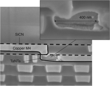
1.1 Cross-section of void in via 3 metal 3 interconnect. Refractory barrier layer is TaNTa. A thin silicon nitride layer is deposited to isolate and encapsulate the copper line. Technology node is 40 nm and current stress is 5 MA cm−2 at 350 °C.
Assuming a copper line of length L, width w and height h, with columnar grain size d, the effective diffusivity is expressed by the contribution of the different diffusion paths:
where δgb and δi are, respectively, the widths of grain boundary and interface. Dlattice, Dgb and Di are, respectively, diffusivity of lattice, grain boundary and interface. The diffusion characteristics of the interface Cu/SiN and Cu/TaNTa are different; this point will be developed in the next part. For clarity, Deff is now simply denoted as D.
The next vacancy flux along the line length in the x direction is composed of Fickian diffusion term and the electromigration driving force term:
The electric field E is replaced by the product of the resistivity ρ times the current density j. The mass transport can now be expressed by the following balance equation:
where R is a sink/source term which represents the generation and recombination of vacancies. Assuming a constant effective diffusivity, from equations [1.5] and [1.6] it follows that a generic one-dimensional transport equation may be expressed by:
Several solutions of equation [1.7] are now reviewed. The first solution provides for the case where Rv is null. This is the form of the equation that was investigated by Shatzkes and Lloyd13 and Clement and Lloyd.14 They investigated the vacancies evolution at the end of a semi-infinite line and in a finite line, respectively. For a semi-infinite line, boundary conditions for the variable Cv are given by Cv(−∞, t) = Cv0 and Jv(0, t) = 0 which means that the concentration at the boundary x = −∞ remains at its equilibrium value and the flux at location x = 0 is blocked. Cv(x, t) solution is given by a Laplace transformation:
where ![]() . Shatzkes and Lloyd suggested that a critical vacancy concentration Cvc was needed to nucleate a void, and thus failure soon followed the nucleation void. Following this statement, equation [1.8] is developed assuming β > > 0, the critical Cvc is reached at time to failure tf:
. Shatzkes and Lloyd suggested that a critical vacancy concentration Cvc was needed to nucleate a void, and thus failure soon followed the nucleation void. Following this statement, equation [1.8] is developed assuming β > > 0, the critical Cvc is reached at time to failure tf:
By using the Arrhenius temperature dependence of the vacancy diffusivity, the time to failure is expressed by:
which is similar in form to Black’s semi-empirical model of equation [1.1] except for the term T2. The predicted time to failure is inversely dependent on the square of current density.
Another analytic solution of equation [1.7] with a null sink/source term and a finite line of length L is now presented. The flux is blocked at both ends of line: Jv(0,t) = Jv(− L, t). The solution is now:
An illustration of the vacancy concentration at x = 0 is proposed in Fig. 1.2 showing the case of a semi-infinite and a finite line. In the calculation, the following set of parameters is chosen: ρ, J, T and Dv are, respectively, 1.6 × 10⁻⁸ Ωm, 2 MA cm−2, 200 °C and 6 × 10⁻¹⁴ m2 s−1.
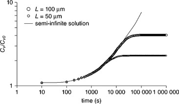
1.2 Accumulation of vacancy at cathode. The symbols correspond to the results of equation [1.11] for two line lengths. The line represents the semi-infinite solution of equation [1.8].
Vacancy concentration is calculated for two different line lengths, the saturation occurs later and at a higher concentration for the larger line than for the smaller one. The semi-infinite solution does not exhibit saturation behavior because the steady state is never reached. Interestingly, the profile of vacancy as a function of diffusion time is not symmetrical with regard to the middle of the line as shown in Fig. 1.3. Indeed the model of transport could be written either in vacancy concentration or atomic concentration because the two species play the same role. The lack of symmetry between accumulation and depletion, respectively, at cathode and anode makes this model inadequate. Concerning qualitative results, the lifetime expected with the formalism described in equations [1.9] and [1.10], at a typical stress condition of 200 °C and 2 MA cm−2 is smaller than that observed experimentally. Because the time to reach the steady state is too short, as observed by Rosenberg and Ohring,15 some improvement on this model is needed.
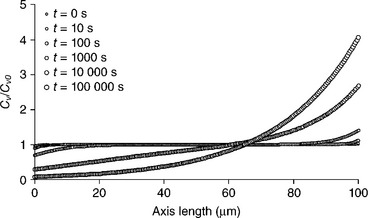
1.3 Distribution of relative vacancy concentration along the line length at different diffusion time.
A new term of source/sink, proposed by Kirchheim,16 is added in the continuity equation.
where Cve is the equilibrium concentration of vacancy with the grain and τ is the average lifetime of vacancy in the grain boundary. Annihilation of grain boundary vacancies occurs if their concentration is higher than equilibrium, and in the opposite case there is generation.
The typical magnitude order of τ is several milliseconds. Assuming that the equilibrium concentration Cve remains constant and close to Cv0, the numerical solution now becomes symmetrical but saturation is incredibly low and the steady state is reached more quickly. As a consequence, a more accurate expression of Cve must be found. Considering that the exchange of vacancies with the grain boundary can contribute to change not only the local equilibrium vacancy in the grain but also the local lattice concentration, a constitutive equation of Cve can be expressed. Two coupled equations need to be solved. Some illustrations of this model were developed by Clement,17 and the solution highlights a plateau before a saturation regime for Cv in function of time. Moreover when τ becomes small, Cv is close to Cve.
Another expression of Rv is now developed. In a metallic line embedded in dielectric, the relative atomic concentration of lattice sites C is related to its hydrostatic stress by:
where B is the effective modulus which depends on the stiffness and thickness of the different materials surrounding the line. The source/sink term can be expressed by:18
On the other hand, the vacancy concentration is in equilibrium with the mechanical stress:
Using the expression of Rv, the equation [1.7] becomes:
Korhonen et al.19 remarked that, in test conditions, the term (CvΩB)/(CkT) < < 1. Such an approximation, leads to the well known equation:
Considering Neumann conditions at both end of the line, Jv(0, t) = Jv(− L, t) = 0, an analytic solution is found:19,20
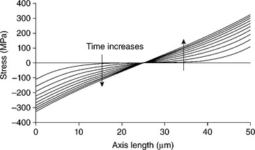
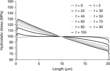
An illustration of equation [1.18] is proposed in Fig. 1.4. For different time steps, the profile of stress along the line is plotted. At the cathode, the accumulation of vacancies leads to tensile stress variation whereas at the anode, the depletion of vacancies leads to compressive stress variation. The stress calculated in equation [1.18] is not representative of the absolute value of the mechanical stress in the line because the mechanical equilibrium is not solved. Thus, it should be taken as the variation of the mechanical stress state from an initial condition.
The equation [1.17] written in stress can also be expressed in vacancy concentration Cv:
This equation is presented in the same form as equation [1.7] without a sink/source term, for which the term BDaΩ/kT is replacing Dv. The consequence is a time-scaling change, so that rather than a lifetime in hours obtained previously in equation [1.7] the lifetime is calculated in days in equation [1.19] (Fig. 1.5). As suggested by Clement,17 diffusion, controlling stress evolution, is a very slow process compared with the build-up of vacancies without considering the role of stress on the recombination/generation of vacancies.
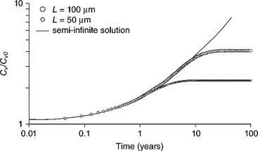
1.5 Accumulation of vacancies at the cathode. The symbols correspond to the results of equation [1.17] for two line length. The line represents the semi-infinite solution. The solution is identical to the one of Fig. 1.2 but the time is rescaled by several decades.
It worth noting that equations [1.17] and [1.19] enable various phenomena not developed here to be explored. The contribution of atomic sinks and reservoirs can be explained with simulation.21 Moreover, by integrating the atoms drifted into the line, the evolution of void volume as a function of time can be assessed; He et al.22 related electromigration lifetime to the saturation void volume. More recently, the effect of grain size was identified, by Dong et al., as playing a role in the maximal stress achieved at the steady state.23
1.2.2 Blech effect
Previous models highlight that when considering only the Fickian term of vacancy and the electromigration term, the time scale of transport was not comparable to the one observed in experiments. Assuming a void nucleation limited by critical vacancy concentration, the time to failure calculated with such simple models fails. When mechanical stress is introduced this shortcoming is resolved.
In 1976, Blech24 and Blech and Herring25 found that mass transport reached a steady state when the conductor length was smaller than a critical value (~ 30 μm) for a given stress condition, below this length, no failure occurs. He observed also that there was no mass transport below a threshold current density. Blech suggested that the presence of a ‘back flow’ of atoms opposite to the electron direction owing to the presence of back stress could explain the steady state regime. If we are considering the flux of a vacancy expressed with the electromigration term, the gradient of mechanical stress is:
This form is the same as in equation [1.19]. The gradient of mechanical stress, referred to as ‘back flow’, opposes the electromigration flux and when the two terms are equal, the net flux becomes null and the steady state is reached. This condition is the Blech condition given by:
Integrating along the line length we find a solution for the stress:
where σ0 is the stress at x = 0. This is a residual stress in the line owing to mismatch of thermal expansion between the line and the surrounding dielectric and process-induced stress.
Assuming a stress yield which corresponds to void nucleation σy the famous critical product for electromigration failure can be expressed by:
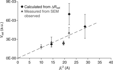
This is also called the Blech product. Typical values for this critical product range from 2500 (copper/low-k) to 6000 A cm−1 (copper/SiO2).26 This model perfectly accounts for experimental results where, under certain j × L stress conditions, electromigration failure does not occur within a reasonable observation time. This situation is currently referred to as ‘immortality’ versus electromigration. However, it is worth noting that, even if stress build-up is likely to generate back flow until total compensation for electromigration flux, a significant amount of metal is moving in the transitory phase. Therefore, depletion on the cathode side results in a resistance change that may or may not reach the failure criteria. The subsequent resistance change ΔR/R will naturally saturate with time to a certain value, (ΔR/R)sat, as described by Filippi et al.27 who demonstrated that, at saturation, the length of the depleted region that contributes to the resistance increase follows a j × L2 dependence.
Moreover, for any given depleted copper trench volume, there is a corresponding given strain to accommodate the excess copper volume increase. In the steady-state regime, the corresponding mechanical stress built-up is function of void volume and initial stress as:
Considering the steady state condition, where back flow totally compensates for electromigration, gives:
This model illustrates that void size, eventually producing an electrical failure, is a function of j × L2. In other words, under a given j × L2 threshold, void size is too small to induce an electrical failure. This model fits experimental observations from Lamontagne et al.28 (Fig. 1.6).
1.2.3 Consequences of the lifetime prediction method
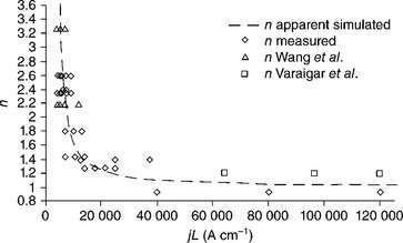
As reported in the previous section, the Blech effect is likely to counteract electromigration so that mass transport is reduced to a certain extent or even totally annihilated. Such phenomena may occur in accelerated electromigration tests as well as in the product in operation. Extrapolation of interconnect lifetime requires an accurate determination of electromigration parameters, which means that any Blech effect should be de-correlated from current density acceleration before projection in operating conditions. Not only can the Blech effect induce an artificial extent of time in a test, but also a misleading determination of the current density exponent. Thus n variation should be expected owing to the nucleation/growth regime, as reported by Lloyd,6 but the Blech effect also affects the apparent value of the current density exponent, as reported by Ney et al.26 in Fig. 1.7.
Ney reported variations in the published values of the current density exponent n that perfectly match the known Blech effect. Similarly, Doyen et al.29 reported continuous variations in the apparent value of the current density exponent, that are likely to affect lifetime projection. In Fig. 1.8, significant deviation from Black’ law with n = 1 is measured for small current density owing to the Blech effect and high current density owing to nucleation and or Joule heating.
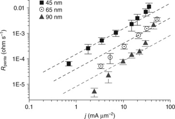
1.8 Evolution of drift velocity with current density, dotted line corresponds to n = 1, for various technology nodes.
After careful determination of electromigration parameters, it is also possible to predict the Blech effect at operations conditions. Ney et al.26 established a simple formalism, deriving from Black’s equation, to take into account the Blech effect in lifetime projection. Not only does the Blech effect make interconnects smaller than a critical length immortal with respect to electromigration, but other short line lifetimes are extended owing to mass flux saturation.
Together with the accurate determination of the j × L threshold, it is important to evaluate the number of interconnect lines that are longer than the above mentioned critical length, as these represent potential electromigration failure locations. In practice, it is quite complicated to run a complete analysis of chip layout owing to the large number of segments.
However, a stochastic model gives an estimation of the number of possible failures, and the scaling factor between interconnect failure rate and chip failure rate. The model proposed by Davis30 expresses the possible combination of logic gates in a chip to create a distribution of necessary lengths to build the aforementioned logic function (Fig. 1.9). This simple model scales the occurrence of potentially failing sites as 1/1000 for a critical length of 100 μm.
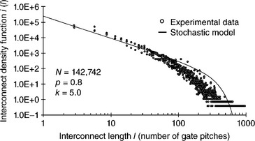
1.9 Distribution of interconnect line length. See reference 30, J.A. Davis, A stochastic wire-length distribution for gigascale integration, IEEE Trans. Electron Devices 45(3) (1998) 580–89. (© 1998 IEEE).
1.3 Numerical methods
Early analytical equations of mass transport described in previous section give insights about electromigration behavior. However only a rough estimate of time to failure equation is given and the immortality criteria (J × L)c can only be applied to simple cases, i.e. simple interconnect geometry. A one-dimensional analytical model is based on many simplifications, and, in particular, it does not take into account the four driving forces involved in the mass transport, nor the complex evolution of void shape during its growth.
Using a multiphysics approach, it is possible to take into account several driving forces to simulate electromigration. The finite element method (FEM) is an appropriate method to solve the case of physically coupled phenomena, such as conduction current, mechanical stress, temperature and diffusion.
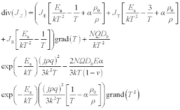
As remarked by Tan and Roy,31 there are two categories of FEM simulation. The first approach consists of a weak coupling calculation of flux divergence from one side and another degree of freedom (temperature, displacement, potential) from another side.32−34 Basically, assuming a constant atomic concentration N, the total mass flux JΣ divergence is expressed by:
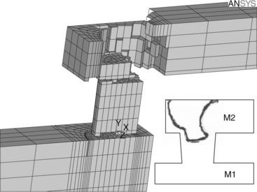
where JE, JT and JS are, respectively, the electromigration, thermomigration and stress migration mass flux. D0 is the self-diffusion coefficient, ρ the resistivity, α the thermal conductivity, Q the heat transport, Ω the atomic volume, E Young’s modulus, α the coefficient of thermal expansion and ν the Poisson coefficient. The temperature, stress and current fields are provided by FEM software and the divergence of JΣ is calculated by an external user routine. A positive mass flux divergence leads to void growth, whereas a negative mass flux divergence leads to hillock formation. If using ANSYS® software, the ‘death birth’ feature enables the user to delete elements of the system which have the highest mass flux divergence. Then a new static field is computed in the line that includes a void. Using this approach deleted elements of the FEM model correspond to the void shape as illustrated in Fig. 1.10. This strategy enables a quasistatic void growth simulation without accurate time to failure assessment because the mass transport equation is not solved.
In the second approach,35−37 all degrees of freedom are solved together. The first approach is numerically easier to handle because quasistatic void growth provides a rough approximation of critical location in the line but the kinetics of the problem are not well represented.
Electromigration, like most of the solid-state reactions or transformations, can be described as the succession of nucleation and growth process steps. The first step consists of vacancy diffusion, which leads to accumulation on the cathode side and depletion on the anode side. When the vacancy concentration (or the stress) reaches a critical value, a void nucleates. The characteristic time τd may not be measurable in practice, because it induces no effect on electrical properties of interconnects. There is no major change in the microstructure and the line resistance remains constant. The second step is the void growth. The resistance change is controlled by the void shape; in practice, measurable resistance change occurs when a growing void reaches the bottom of the metal line. Moreover, the diffusion barrier acts as shunt resistance, but as it is very resistive, a abrupt resistance step is usually recorded (Fig. 1.11).38 The characteristic time is τf, the time to failure, which is therefore a result of the diffusion rate and void shape.
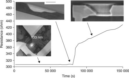
1.11 Typical evolution of resistance during electromigration testing of copper interconnect, through various steps of void nucleation and growth. See reference 38, X. Federspiel, D. Ney, L. Doyen, V. Girault, Dynamics of resistance evolution during electromigration stress, IEEE International Integrated Reliability Workshop (2006), 24–27. (© 2006 IEEE).
In the following section, vacancy transport mechanisms are reviewed. The nucleation phenomenon is studied thanks to continuum physics, without using ‘birth of void entities’ concepts in the copper material, i.e. after reviewing the governing equation and the associated physics, some illustrative results are presented.
1.3.1 Vacancy transport constitutive equation
Assumptions are similar to those from part 1.2.1. The microstructure of copper is not taken into account. As atomic diffusion is the result of a vacancy exchange mechanism, the effective vacancy diffusivity Dv is given by:
where Ca/Cv and Da/Dv are, respectively, the concentration of vacancies/ atoms and the diffusivity of vacancies/atoms. Typically, at 200 °C, the Cv/Ca ratio is roughly 10−7.
The electron wind force alone is insufficient to quantitatively describe the mass transport. Other contributions are included in the electrochemical potential and is taken as:
where μ0, μE, μT, μC and μS are, respectively, the electrochemical potentials related to the reference state, electromigration, thermomigration, concentration and stress migration. The driving force F derives from the electrochemical potential, F = − grad(μ), and the net vacancy flux Jv along the line is a function of the driving force:
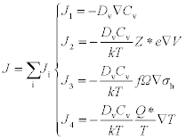
The total vacancy flux J is the sum of four contributions:
Adding the Fickian term J1, the flux depends on the gradient of the hydrostatic stress σh (J3), temperature T (J4) and potential V (J2). Assuming that a vacancy behaves like a substitutional foreign atom in the copper lattice, but with a smaller volume, the vacancy volume relaxation is given by the f ratio in J3. The transport heat Q* in J4, is the isothermal heat transmitted by moving the atom in the process of jumping a lattice site.
Moreover, the generic form of vacancy diffusivity Dv is assumed to be characterized by an exponential dependence on the hydrostatic stress39 and temperature:
where Dv0 is the prefactor and Ea is the activation energy of vacancy diffusion. The vacancy concentration is driven by a general diffusion equation, with G a source/sink term:
Usually, the source/sink term describes the production of vacancies when their concentration is larger than the equilibrium value whereas the opposite case describes the annihilation of vacancies:
where τv is the characteristic generation/annihilation time, Ev the activation energy of vacancy formation and Cv0 the equilibrium vacancy concentration in the absence of stress and at zero kelvin.
Assuming that grain boundaries play an important role in the generation and annihilation of vacancies, Ceric et al. suggested another equation set.40 The source/sink term G is now expressed as a function of the incoming and outcoming fluxes through the grain boundary, respectively, Jv,1 and Jv,2, and δ the grain boundary thickness.
where the incoming and outcoming fluxes are expressed by:
where ωT is the trapping rate of vacancies in the grain core, ωR the release rate, Cvim the trapped vacancy concentration and Cveq the equilibrium vacancy concentration in the grain boundary. Finally the conservative mass balance from equation [1.31] is solved by coupling the corresponding current Laplace equation, [1.35], the equilibrium mechanical equation, [1.36], and the Fourier thermal equation, [1.37], as follow:
where ρ and k, respectively, are the electrical and thermal conductivities. Equations [1.31], [1.35], [1.36] and [1.37], are solved simultaneously in the transient state. For numerical reasons, equation [1.31] is solved with normalized concentration N in order to simplify the initial condition:
At the initial time ti (before applying current), the initial hydrostatic stress field is σhi and the initial temperature is Ti.
1.3.2 Mechanical constitutive equation
The difference between the volume of an atom and the volume of a vacancy leads to a volumetric strain, similar to a thermal expansion-induced stress. In the general framework of small deformation formulation, the strain rate partition in an elementary volume is expressed as:
The total strain rate is the sum of the elastic strain rate, the thermal strain rate, the viscoplastic strain rate and the electromigration strain rate parts. After copper annealing, the cooling down to room temperature leads to a residual stress state owing to a coefficient of thermal expansion mismatch:
where α is the coefficient of thermal expansion and δij is Kronecker’s symbol.
Several theoretical models have been proposed to describe electromigration-induced stress evolution. Initially, Povirk41 and Rzepka et al.42 considered that mass accumulation or depletion leads to the following strain rate.
The Sarychev et al.43 approach considers the source term. The electromigration strain rate part has two origins: the first is the vacancy flux divergence and the second is the vacancy generation/annihilation. Equation [1.42] expresses the diagonal tensor; a detailed demonstration was given by Sarychev et al.43
It is assumed that when an atom moves under electromigration forces it leaves behind a vacancy. There is a local spherical symmetry strain field induced at that lattice site owing to the difference between the volume of an atom and the volume of a vacancy.
The last term in equation [1.42] is the viscoplastic part. Constitutive material behaviors of copper or aluminum have been investigated.44,45 In a simple expression of Coble creep controlled by electromigration-induced grain boundary diffusion suggested by Li and Dong,46 the creep rate dependence with current density is linear. More generally, viscoplasticity flow could be modeled by a power law of the von Mises stress invariant M(σ), with a threshold R0. With the convention < a > = max(a,0), the viscoplastic strain rate tensor is written as:
where s is the deviatoric part of the stress tensor. The threshold R0, n and the parameter K of the Norton law are temperature independent but K could have a Arrhenius dependence.
For electromigration of solder alloys, Tang and Basaran,47 Kashyap and Murty48 and Basaran et al.49 use the same form of viscoplastic flow with a kinematic hardening term because, in this case, fatigue loading and thermal cycling effects are significant. Extraction of material parameters for thin films as used in interconnects is quite challenging and a calibration of copper viscoplastic flow law is still not available. Thus, the viscoplastic part is not included in the following development. However, it has been highlighted that plasticity build-up, more precisely dislocation cores, play an important role as fast diffusion paths. The so-called ‘pipe diffusion’ would amplify diffusivity, and thus affect the MTF.50
Sarychev’s work inspired various studies51,52 and it enables stress evolution to be simulated in two-dimensional (2D) structures, where a homogeneous diffusion medium without any preferential diffusion path is considered. Sukharev et al.53 and Sukharev54 distinguished the different diffusion paths for the interface and the bulk. They assumed two different vacancy concentrations Cint and Cbulk, and thus two continuity equations are solved:
The interface means the grain boundaries, the interface Cu/SiN, the diffusion barrier Ci/TaNTa for which a higher diffusivity coefficient Dv is imposed than the bulk one. Plated atoms are exchanged between bulk and interface, so vacancy generation or annihilation is represented by atom plating or removal from the grain boundary. The source/sink has a standard form:
If we are considering that the plated atoms are immobile and are defined by a concentration Ca, the plated atom continuity equation for bulk and interfaces is given by:
Sukharev56 suggested that the diagonal term of electromigration-induced strain tensor is expressed by:
where Ca0 is the concentration of atoms in the plated copper layer without mechanical stress. Sukharev concludes that the evolution of atom concentration in the plated layer is mainly responsible for stress build-up. However, such an approach implies the resolution of several degrees of freedom, Cvint, Cvbulk and Caint. The definition of the interface domain with a representative thickness is a strong limitation to this modeling strategy. Meshing fine domain with a high aspect ratio thickness/surface is known to induce a very large number of elements in FEM problems, this approach seems to be limited to 2D problems.
1.3.3 Application to evolution of stress in metal lines
Model and boundary conditions
A 2D FEM model is used to simulate vacancy transport in a copper line embedded in oxide. The electromigration testing conditions are representative of a package level test: the sample is maintained at uniform temperature, stress current density being small enough so that Joule heating and the subsequent temperature gradient in the system is not significant. As depicted in Fig. 1.12, in the present simulation, boundary conditions and initial conditions are set as follows:
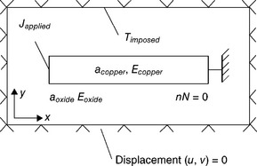
1.12 Schematic illustration of the boundary conditions for various degrees of freedom: temperature, current and displacement.
• A current density in copper is set to 1 MA cm−2. The temperature gradient is neglected and conductivity is assumed to be constant.
• Temperature is set to 340 °C in the external domain of the oxide.
• The system is assumed to be in a plane strain state. An initial hydrostatic stress state of 100 MPa (owing to a mismatch of thermal expansion coefficients between copper and oxide) is assumed at the considered temperature.
• Concerning vacancy diffusion, Neumann conditions at the copper/ oxide interface are set in order to ensure the conservation of the total number of vacancies N. Effective copper diffusivity is assumed to be constant in the whole structure. Equation [1.38] gives the field of initial concentration.
Results
Simulated evolution of stress and relative vacancy concentration are now presented for both 20 and 200 μm length copper lines. The results should be considered as qualitative. Moreover, the proposed model simulates stress evolution disregarding nucleation steps. However, the results of this simulation allow to evaluate the relevance of hypothesis of simpler models presented previously. First, despite the fact that the problem is formulated in two dimensions, the vertical total flux Jy is negligible compared with Jx as shown in equation [1.29]. As a consequence, the actual model could be reduced to a one-dimensional (1D) problem. Moreover, in such conditions, the four driving forces described in equation [1.29] do not act with the same weight:
Therefore, qualitatively, at the cathode, high vacancy accumulation occurs, whereas there is depletion at the anode. Moreover, the hydrostatic back stress becomes increasingly tensile at the location of vacancy accumulation and it is more compressive at the location of vacancy depletion. Because of the low stiffness of oxide, stress in copper is partially relaxed in the vicinity (< 1 μm) of the copper/oxide interface, therefore a stress gradient and concentration gradient develops from the center to the edge of the line. However, from the early beginning of diffusion, an equilibrium occurs at the cathode, so that this area, which is initially in depletion, starts to accumulate vacancies.
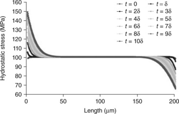
The evolution of stress in the 20 and 200 μm lines is shown, respectively, in Figs. 1.13 and 1.14, with the same time scale, i.e. δ = 1000 s. For short lines, the back stress flux soon compensates the electromigration flux, and the steady state is reached. The steady state is reached when only a small amount of metal is effectively diffused, so that no void big enough to induce electrical failure is formed; this situation is referred to as ‘immortality’ behavior according to the Blech approach. On the other hand, for long lines, the stress drastically rises and reaches a critical value, thus allowing void formation and growth. However, it is likely that the void nucleation would locally modify the boundary conditions of the problem. The void nucleation stress is estimated to be 40 MPa for copper55 and 500 MPa for aluminum.56
The evolution of the concentration N at the cathode is summarized in Fig. 1.15 for two line lengths (20 and 200 μm), and two current densities (1 and 3 MA cm−2). At this location, the stress is partially relaxed and so N is close to one. A small current density in a small segment leads to a very low value of vacancy saturation, as the steady state is reached. In a given segment, when increasing the current, the accumulation is enhanced and occurs earlier. Moreover, for a long segment, N may be increased by a factor 10, because the total vacancies Nt available for diffusion is much more important.
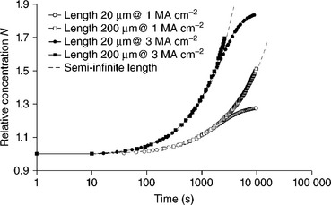
1.15 Evolution of the concentration N, at the cathode for two segment lengths and two current densities.
An in-depth analysis of Fig. 1.14 shows that the stress field is not perfectly symmetric. This can also be observed in concentration distribution, which is not precisely shown here. On the other hand, migration kinetics are slightly accelerated at the cathode and slowed down at the anode. This subtle difference results from stress diffusivity dependence, see equation [1.30]. This model is rather simplified: the diffusion paths, the texture-induced stress localization and the current concentration under via are not taken into account here and will be analyzed in a later section.
1.3.4 Application to real circuit layout case
In this section, we present a 2D simulation of a real circuit layout and analyze the consequences of the Blech effect on circuit lifetime and dc current design rules. Moreover, dc electromigration rules, as used in semiconductor industries, are commonly described as maximum current allowed in a metal line with vias at each end. The maximum current in operation is fixed disregarding the number of connections to this line as well as any variation of current along the line. As described in the previous section, the Blech effect is likely to slow down or totally stop the electromigration flux when the j × L product is under a certain threshold. This picture is simple to analyze in an elementary line under constant current but it is not directly applicable to complex interconnection.
As an example of a complex interconnection tree, we defined a simplified model of a power grid where the main line is feeding current to various blocks connected along the line through single vias (see Fig. 1.16). Several cases were simulated, making the number of vias along the line varying, as well as changing the current i.e., constant current density in feeding vias (line end) or constant current in vias connected to blocks (Japplied in Fig. 1.16). Simulation results for the vacancy concentration profile in the line for the stationary regime are plotted in Fig. 1.17. The hazard of electromigration failure is assessed according to the vacancy profile or stress profile. The nucleation and growth of a void is not taken into account, but the evolution of vacancy concentration is interpreted as the amount of potential void volume. Using this figure of merit, we compared a simple metal line with a power grid.

1.16 Illustration of simplified power grid layout, line M1 is supplied by two stacked vias (left). Vacancy transport is simulated in line M1 assuming that all contacts delivered the same current Japplied (right).
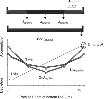
1.17 Comparison of vacancy profile in single metal line and power grid case, for constant feeding current and total length.
From Fig. 1.17, it appears that the maximum vacancy concentration is lower in the power grid than in the simple line case. In other terms, the effective length corresponding to the Blech effect is not the total line length, but rather depends on the local current density and flux divergence. As a consequence, the dc current rule could be relaxed by a certain factor after accurate simulation of the real layout.
1.3.5 Application to diffusion path and texture effects
Model and boundary conditions
The purpose of this three-dimensional (3D) model is to simulate electromigration in a metal line containing a significant number of copper grains whose crystalline orientation reflects the (111) texture, i.e. the copper grains are (111) oriented along the z-axis and randomly oriented in the plane x-y. Grain size is set to the order of line width to simulate the ‘bamboo’ case, and line length is set to 2 μm, which means that the line is ‘immortal’ with respect to the usual Blech criteria. The line is embedded in dielectric and connected to metal vias so that mechanical and electrical 3D effect can be simulated. Copper has a fcc structure and its elastic properties are defined thanks to three constants, like any cubic element: C11 = 168, C12 = 121 and C44 = 75 GPa.
At the temperature of the electromigration test, the thermal expansion between the oxide and the copper leads to a large inhomogeneity in the shear stress state owing to the anisotropic elasticity use. Indeed, strong grain disorientation leads to an important stress gradient, including a zone in compressive stress, whereas the average stress is tensile. The Von Mises stress state before applying current is shown in Fig. 1.18. Moreover, the gradient of stress and current density concentration are particularly high at the vicinity of the via/line interface. In this location, the current crowding creates an electromigration flux divergence, which is also a mechanical singularity at the interface copper line/via.
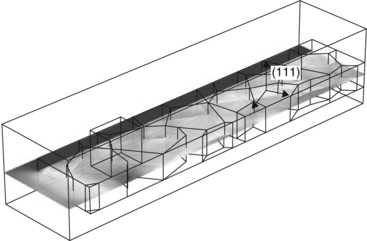
1.18 Map of von Mises component in cross-section of a copper line before the current stress. Grains are (111) textured.
The copper/capping interface has been reported as a fast diffusion path for electromigration.57 However, in this model, all the possible different diffusion paths are taken into account, i.e. the copper/capping interface, the copper/diffusion barrier interface, the grain boundary and bulk diffusion and are noted as 1, 2, 3 and 4 in the following. Equation [1.31] with Dv4 and the boundary conditions involve the diffusivity Dv1, Dv2 and Dv3. In practice, the diffusivity coefficient is quite difficult to measure, because it is highly dependent on the impurities concentration and process parameters. However, the activation energy is found to be 2.15 eV for bulk copper,39 1.2, 0.92 and 0.85 eV for the grain boundary57−59 and 1.06, 1 and 0.8 eV for interfaces.60 In our model, diffusivity prefactors are set as following:
The first diffusion paths are the copper/capping and copper/diffusion barrier interfaces. The ratio between all diffusion paths is consistent with reported nucleation of electromigration voids. Moreover, void nucleation is frequently reported to occur next to the via at the triple point between, the barrier/copper and the copper/capping interface, where a strong flux divergence is expected to occur.
Results
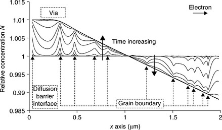
In the initial condition, the concentration N is quite constant inside the line; indeed the hydrostatic stress is quite homogeneous. Then, concentration quickly increases in paths 1, 2 and 3, and finally bulk grain concentration is affected.
Because of the field of vacancy concentration shown in Fig. 1.19, vacancy accumulation occurs at the cathode, through paths 1, 2 and 3, whereas grains under the via are close to equilibrium concentration N ~ 1. In addition, it is remarkable that the grain boundary under the via, which is perpendicular to the line and main transport direction, plays an important role in vertically carrying vacancies from the bottom of the interface towards the via.
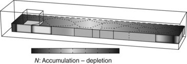
1.19 Field of vacancy concentration in the line in transient state, diffusion follows different paths: interface, grain boundary and lattice.
Although path 4 (bulk) plays a minor role in the transient regime, and is not a limiting factor for the overall electromigration dynamics, it eventually controls the concentration gradient inside grains. In Fig. 1.20, we plotted vacancy concentration across several grains, for different time steps. The concentration profile shows sharp oscillation through neighboring grains that converge to form a smooth profile in a steady state value. The concentration gradients are sharper in small grains than in large grains. The grain boundary and the interfaces act as sink/sources for vacancies to maintain concentration in the bulk at the equilibrium. In other words, G described in equation [1.32], should be rewritten for the different diffusion paths with a characteristic time following: τ1 < τ2 < τ3 < < τ4.
1.3.6 Morphological void evolution
The dynamics of electromigration-driven void growth in solid metals is a wide research field and a challenging theoretical problem.61 Capillary forces as well as electrostatic and electro-mechanical forces are involved in interface motion and morphology evolution. Various aspects of void morphology evolution are reviewed in the literature,62−66 the electron wind promotes the formation of slit-shape voids, whereas surface driven void growth leads preferentially to round shapes. Therefore, the final shape will result from the initial shape as well as surface diffusivity and surface free energy. The evolution of void shape involves different processes, as its migration along the line is affected by the microstructure, with subsequent growth and collapse or the agglomeration at a particular location. Although fundamental understanding of void dynamics remains difficult, we review two types of interface modeling approach. In the first approach, the interface in the solid is represented as the ideal perfect sharp boundaries for which the front (interface void/metal) is explicitly computed and updated. In the second approach, an implicit function represents a smooth interface.
Sharp interface approach
The void motion is controlled by an atomic diffusion process along the void/ metal interface. The diffusion of atoms lying on the crystal surface, known as adatoms, is faster than bulk diffusion. The chemical potential of an adatom in the interface is
where μ0 is the reference value of the potential, Ω is the atomic volume, γ is the interface energy, κ is the local curvature of the interface, Z*e is the effective charge and E is the electrical applied field. The atomic flux along the interface is caused by the gradient of the chemical potential:
where ∇s is the surface Laplacian, δs is the interface thickness, Ds is the interface diffusivity, and Es is the tangential electrical field to the interface. The normal velocity is then expressed by:
This last equation implies mass conversation and thus the conservation of the void size during important morphological void changes.62
Early analytical solutions provide asymptotical behavior. Assuming isotropic material properties and an infinite metal line, the analytical solution to this problem show that the motion velocity of a spherical inclusion is proportional to the applied electrical field and inversely proportional to the void size.67 For a circular void shape, the normal velocity is given by:
where d is the void diameter, and E0 is the applied electric field. The same development was established by Li and Chen for an elliptical void.68 More general formulations are developed including diffusion anisotropy and current crowding owing to confinement.69 However, numerical methods are preferred for modeling the void evolution. As mentioned before, sharp interface modeling implies that the function describing the interface void/ metal is explicit and special techniques are used for the front tracking.
Kraft and Arzt70 used a numerical scheme which combined the FEM and the finite difference method (FDM). The FEM provides the temperature, whereas electrical field near the void and FDM provides the front normal velocity. The remeshing and field transfer procedure is performed iteratively. The assumption of constant void size means that there is no species exchange between the void/metal interface and mass transport inside the line. Consequently, the simulation is independent of line length therefore unable to reproduce the Blech effect. Kraft uses another definition of normal velocity which does not imply volume conservation. A low growth rate leads to slit-like voids whereas for higher rates it leads to wedge-shaped voids.
This modeling approach was improved for introducing anisotropic diffusion.71 Indeed, simulation by the first principles method shows that the diffusion barrier energy of adatom on copper (001), (110) and (111) surface is, respectively, 0.68, 0.56 and 0.07 eV.72 More recently, the dynamic response of the void morphology driven by surface electromigration was investigated and the effect of the electrical field, surface diffusion anisotropy and void size was examined.73,74 The anisotropy of the surface adatom diffusivity is expressed by:
where Ds,min is the minimum surface diffusivity and θ is the angle between the local tangent to the void surface and the applied field direction. A, m and ϕ are parameters that, respectively, determine the magnitude of the surface diffusivity anisotropy, the degree of anisotropy and the misorientation of a symmetry direction of fast surface diffusion with respect to the electrical field direction. Following the magnitude of the different contributions (electrical field, surface diffusion anisotropy or void size), some transitions from steady state to stable oscillatory morphological evolution can exist.75 These transitions are the results of Hopf bifurcation at the corresponding critical point. The nature of the Hopf bifurcation is determined by the symmetry of the surface diffusion anisotropy and the bifurcation is supercritical and subcritical for fourfold (m = 2) and twofold (m = 1) symmetry, respectively. In addition, in symmetry cases, hysteresis phenomena and bistability was simulated. Illustration of different void morphological evolutions is presented in Fig. 1.21. The evolution of void surface area with particular model parameters has a oscillatory behavior and may be suddenly unstable.
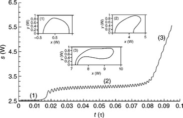
1.21 Evolution of void surface area per unit film thickness s from an initial configuration with semi-circular cross-section on the plane of the film. The insets to the figure show void morphologies representative of the three stages in the void morphological evolution, (1), (2) and (3), characterized by the absence of surface oscillations, oscillatory dynamics, and the necking instability.75
Another point is the mechanical stress effect on the evolution of void morphology.76 The normal velocity is modified to:
where w is the elastic energy density derives from a FEM solution. The consequence is that an initial circular void remains circular if the surface energy γ has an important weight. On the other hand, if the electromigration term or elastic density energy is the major contributor, the void may collapse into a slit or present severe instability. Application with 3D simulation was demonstrated by Zhang.77
The interaction between grain boundary diffusion and void motion was simulated by Bower and Shankar78 with a sharp interface approach. The model includes grain boundary sliding, grain boundary diffusion, grain boundary migration and surface diffusion. According to the gradient of chemical potential, atoms can detach from the grain, diffuse along the boundary and re-attach to another grain or surface. The flux of the atoms tangent to each interface is the same as in equation [1.50] but the gradient of the normal stress component to the boundary is added. Several phenomena were simulated; the void may remain connected to the grain boundary while both the void and grain boundary migrate together down the line; the void may migrate and detach from the grain boundary; the void may grow or shrink, while migrating with or without the grain boundary. For the sake of illustration, the case of a void released from a grain boundary79 is shown in Fig. 1.22. The surface evolves much faster than the grain boundary and consequently the void de-pins from the grain boundary. On the other hand if the surface and the grain boundary migrate at similar rates the void remains pinned at the grain boundary.
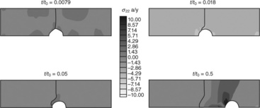
1.22 Void escaping from a grain boundary.79
Finally, the shape interface method is attractive for describing complex void shape dynamics. Its enables us to accurately investigate the consequence of a local property of the interface on the void surface evolution. However, the explicit function of the interface needs to be continuous whatever the evolution of the void (bistability, void collapse, etc.). Front tracking is generally difficult to handle, it may require re-meshing and field transfer procedures. While this method is efficient for 2D geometry, the generalization to 3D geometry is challenging.
Diffuse interface approach
In the diffuse interface approach a phase field is solved and the interface corresponds to the zero contours of the phase field. Thus, the void surface is implicitly represented by an order field parameter. The field parameter ϕ takes the value − 1 and + 1, respectively, in the solid and void phase. It has a smooth evolution inside the interfacial medium between the two phases. The evolution of the phase field is governed by the Cahn–Hilliard equation. Some illustrations have been proposed.79−81 It is noticeable that the adaptative mesh procedure is necessary during the simulation, fine element size is needed in the narrow interfacial domain and the element size is relaxed elsewhere for the computation of the mechanical and electrical fields. This strategy seems to be very resource consuming and not adequate for 3D geometry. The level set method is preferable. The idea of evolving an interface by representing it as a level set of a field function was introduced by Osher and Sethian.82 The interface ![]() is implicitly represented as the one half level of a continuum function ϕ. The interface is defined as follows:
is implicitly represented as the one half level of a continuum function ϕ. The interface is defined as follows:
where the ϕ function ranges from 1 to 0, that corresponds respectively to the metal and the void phases. With the normal velocity vn of the interface, ϕ evolution is given by a Hamilton-Jacobi equation:
Shape change or drift along the metal line of the void surface is caused by adatom diffusion. The interface velocity caused by electromigration flux is usually assumed to be proportional to the component of the electrical field tangent to the surface and the chemical potential gradient along the void surface. Assuming mass conservation, the normal component of velocity at any point of the surface is given by:
where γ is the surface energy, κ is the local curvature of the surface and s is the interface arc length. With this formulation of normal velocity, the shape of the initial void was investigated and it was demonstrated that the electric field strength drives the morphology of the void, and that at higher current density, slit-like shape voids may occur. Note that γ and Ds may be anisotropic, and the details are available in other studies.83
Another definition of vn is preferred. Indeed, the major drawback of equation [1.57] is that no exchange between adatom diffusion in the void surface and the vacancies in the metal line is considered. To circumvent this limitation, a coupling between the vacancy transport equation and the surface motion is performed. Hence, the vacancy flux Js at the void surface s is expressed as:
δ(ϕ) is the smooth δ-function of ϕ, ∇s is the surface gradient operator, the global vacancy diffusivity can be rewritten:
The diffusion equation is modified in order to consider the interface flux Js:
Finally, the normal velocity depends on the local vacancy concentration rate:
where K, a physics-based constant, is temperature independent and arbitrarily set in the model. At the void interface, if the vacancy concentration reaches a yield value N0, the normal velocity becomes negative. As a consequence, a concave or convex interface tends to respectively grow or shrink the void. The classical formulation of the interface velocity, as defined in equation [1.57], and the velocity based on vacancy concentration rate equation [1.61], may provide distinct void shape results.
In the next section, the model using equation [1.61] is applied to a practical case of electromigration in a copper line. However, for the sake of simplification, the drift of voids is not addressed. Therefore, assuming that vn = min(vn, 0), only the irreversible process of void growth is simulated.
Application to void growth
After discussing void dynamics, the aim of this application is to investigate the electrical signature during void growth. For the sake of simplification, a 2D model is built. The copper line length is 250 μm and grains are not explicitly represented. The fastest diffusion path is represented by the capping layer. The electrical conductivity of the 6 nm diffusion barrier is described; and the ratio between the resistivity of the diffusion barrier and copper is assumed to be 170. The package level test is performed at 300 °C, and the applied current density is 3 MA cm−2.
The evolution of the simulated void growth, Fig. 1.23, and the electrical resistance change, Fig. 1.24, are simultaneously discussed:
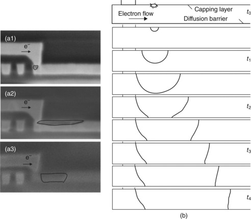
1.23 (a) Cross-section of void in copper for various samples at the same time of electromigration test; (b) sequence of simulated void growth at different times of electromigration test.
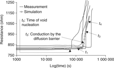
1.24 Evolution of the resistance during the electromigration test. The different lines represent a set of experimental measurements.
• After a first step of vacancy transport suggesting void location, a small void is artificially introduced in the capping layer at a distance of 80 nm in front of the via, as seen in Fig. 1.23b at time t0. No significant resistance change is observed during this period (Fig. 1.24).
• Then, at time t1, the front grows in both vertical and lateral directions. As a consequence, the electrically conducting section is reduced, and hence the resistance smoothly rises.
• Once the bottom front of the interface reaches the diffusion barrier, the global line resistance drastically rises as shown in time t2. Indeed, the electrical resistivity of the diffusion barrier is much higher than the copper one.
• Finally, the void grows at the side where vacancies are released by the capping layer. However, the other side of the front cannot move because vacancies do not have any diffusion path to reach this front. Time t3 and t4 correspond to a linear resistance rise; the slope of this regime enables a direct measurement of the drift velocity and can be used to determine the activation energy and the current density exponent.
Some observations of voids on different samples are presented in Fig. 1.23a: the case of an initial void located under the via (see Fig. 1.23a1) leads to an abrupt resistance rise and to a short-circuit in the conducting line, because the electrical path is not available anymore. Otherwise, the void is usually nucleated in the capping layer in front of the via and grows both vertically and along the capping layer interface (see Fig. 1.23a2 and Fig. 1.23a3).
However, the electrical signature of a measurement set is not as simple as the one found in the simulated case. Indeed, several mechanisms, such as void coalescence and void trapping, which are not represented by the model, play an important role. Moreover the dispersion in terms of failure times, attributed to texture effects and process variability is not addressed.
1.4 Conclusion
From the simplest phenomenological MTF expression to the more sophisticated multiphysics simulations, the different modeling techniques are reviewed. The analytic solutions provide the profile of the hydrostatic stress or vacancy concentration along the line, regarding different assumptions of the vacancy generation and annihilation term in the grain core or in the grain boundary. For a time to failure limited by nucleation or growth, this approach can only be applied on a simple system. However, the basic nucleation criteria, which have not been developed here, remain rather complex to experimentally characterize. With the help of CPU resource democratization, simulations based on multi-driving forces have emerged in the past few years. Different numerical schemes have been developed for simulating the evolution of void shape during electromigration. Correlation with the electrical resistance profile makes the simulation qualitatively correct with regard to the time scale and the final void size.
Simulation of electromigration is a field under development and it is noticeable that new promising approaches are emerging. Physics-based predictive Monte Carlo simulation is able to model void incubation, its coalescence and void growth,84 a physical MTF formulation being derived. Atomistic Monte Carlo simulation is suitable to deal with interatomic interaction under electromigration85 or atomic drift/diffusion in the grain boundary.86 Interestingly, the shape evolution of a void simulated by continuum theory matches the one given by kinetic Monte Carlo simulation in certain conditions.87 The peridynamic approach has been recently derived from the multiphysics simulation of electromigration. Contrary to the classical continuum mechanics and transport equation, this approach has the advantage that the response fields do not need to be differentiable, and it is well adapted to handle the boundary conditions at the void surface.88
With the increasing complexity of models, the number of unknown parameters is becoming important. There are many parameters of the models that are difficult to address experimentally, such as interface properties, effect of microstructure and texture. Consequently, simulation is difficult to calibrate and so models are still not able to predict time to failure. Moreover, the simulation of void growth for various line lengths, current densities or temperatures does not cover all the reported failure cases with a unique set of equations. However, the simulated stress distribution and the Blech effect successfully match experimental observations and are particularly useful for the optimization of circuit layout. In addition, it is possible to simulate various void shapes and the resulting electrical resistance to track critical failure modes. Finally, dispersion of measured parameters, such as MTF and post-mortem void size, is a strong limitation for model calibration but also an innovative field of investigation. Indeed, MTF spread is drastically reducing design margins and circuit robustness, therefore the simulation is suitable to explore the root cause of macroscopic dispersion.
1.5 References
1. Fiks, V.B. On the mechanism of the mobility of ions in metals. Sov. Phys. Solid State. 1959; 1:14.
2. Huntington, H.B., Grone, A.R. Current-induced marker motion in gold wires. J. Phys. Chem. Solids. 1961; 20:76–87.
3. Mass transport of aluminum by momentum exchange with conducting electrons. Proc 6th Ann. Reliab. Phys. Symp. 1967; 148–159.
4. Black, J.R. Electromigration – a brief survey and some recent results. IEEE Trans Electron Devices. 1969; 16(4):338–347.
5. Black, J.R. Electromigration failure modes in aluminum metallization for semiconductor devices. Proc. IEEE Letter. 1969; 57(9):1578–1594.
6. Lloyd, J. Black’s law revisited – nucleation and growth in electromigration failure. Microelectron. Reliab. 2007; 47:1468–1472.
7. Clement, J.J. C.V Thompson, Modeling electromigration-induced stress evolution in confined metal lines. J. Appl. Phys. 1995; 78:900.
8. Lloyd, J. Electromigration failure. J. Appl. Phys. 1991; 69(11):7601–7604.
9. Kirchheim, R., Kaeber, U. Atomistic and computer modeling of metallization failure of integrated circuits by electromigration. J. Appl. Phys. 1991; 70(1):172–181.
10. Basaran, C., Lin, M., Ye, H. A thermodynamic model for electrical current induced damage. Int. J. Solids Struc. 2003; 40(26):7315–7327.
11. Montemayor-Aldrete, J.A., Vázquez-Villanueva, C., Ugalde-Vélez, P., del Castillo-Mussot, M., Vázquez-Fonseca, G.J., Mendoza-Allende, A., Coyotécatl, H.A. Non-equilibrium statistical theory for electromigration damage. Phys. A, Stat Mech. Appl. 2008; 387(24):6115–6125.
12. d’Heurle, F.M. Electromigration and failure in electronics: an introduction. Proc. IEEE. 1971; 59:1409–1418.
13. Shatzkes, M., Lloyd, J. A model for conductor failure considering diffusion concurrently with electromigration resulting in a current exponent of 2. J. Appl. Phys. 1986; 59:3890–3893.
14. Clement, J.J., Lloyd, J.R. Numerical investigation of the electromigration boundary value problem. J. Appl. Phys. 1992; 71:1729–1733.
15. Rosenberg, R., Ohring, M. Void formation and growth during electromigration in thin films. J. Appl. Phys. 1971; 13:5671–5679.
16. Kichheim, R. Stress and electromigration in Al-lines of integrated circuits. Acta. Metall. Mater. 1992; 40:309–323.
17. Clement, J.J. Electromigration modeling for integrated circuit interconnect reliability analysis. Trans. Dev Mater. Reliab. 2001; 1(1):33–42.
18. Clement, J.J., Thompson, C.V. Modeling electromigration-induced stress evolution in confined metal lines. J. Appl. Phys. 1995; 78:900–904.
19. Korhonen, M.A., Borgesen, P., Tu, K.N., Li, C.-Y. Stress evolution due to electromigration in thin film. J. Appl. Phys. 1993; 73:3790–3799.
20. Carlow, H.S., Jaeger, J.C. Conduction of heat in solids. Oxford, UK: Clarendon; 1947.
21. Wei, F.L., Hau-Riege, C.S., Marathe, A.P., Thompson, C.V. Electromigration-induced extrusion failures in Cu/low-k interconnects. J. Appl. Phys. 2008; 103:023529.
22. He, J., Suo, Z., Marieb, T.N., Maiz, J.A. Electromigration lifetime and critical void volume. Appl. Phys. Lett. 2004; 85:4639–4643.
23. Dong, X., Zhu, P., Li, Z., Sun, J., Boyd, J.D. Electromigration-induced stress in a confined bamboo interconnect with randomly distributed grain sizes. Microelectron. Reliab. 2010; 50:391–397.
24. Blech, I.A. Electromigration in thin aluminum films on titanium nitride. J. Appl. Phys. 1976; 47(4):1203–1208.
25. Blech, I.A., Herring, C. Stress generation by electromigration. Appl. Phys. Lett. 1976; 29(3):131–133.
26. Doyen, L., Petitprez, E., Waltz, P., Federspiel, X., Arnaud, L., Wouters, Y. Extensive analysis of resistance evolution due to electromigration induced degradation. J. Appl. Phys. 2008; 104:123521.
27. Filippi, R.G. The effect of current density, stripe length, stripe width, and temperature on resistance saturation during electromigration testing. J. Appl. Phys. 2002; 91:5787–5789.
28. Lamontagne, P., Doyen, L., Petitprez, E., Ney, D., Arnaud, L., Waltz, P., Wouters, Y. Cu interconnect immortality criterion based on electromigration void growth saturation. IEEE International Integrated Reliability Workshop. 2009; 56–59.
29. Ney, D., Federspiel, X., Thomas, O., Gergaud, P. Stress induced electromigration backflow effect in copper interconnects. IEEE Trans. Device Mater. Reliab. 2006; 6:175–180.
30. Davis, J.A. A stochastic wire-length distribution for gigascale integration. IEEE Trans. Electron Devices. 1998; 45(3):580–589.
31. Tan, C.M., Roy, A. Electromigration in ULSI interconnects. Mater. Sci. Eng. R. 2007; 58:1–75.
32. Dalleau, D., Zaage, K.W. Three-dimensional voids simulation in chip metallization structures: a contribution to reliability evaluation. Microelectron. Reliab. 2001; 41:1625–1630.
33. Tan, C.M., Roy, A. Investigation of the effect of temperature and stress gradients on accelerated EM test for Cu narrow interconnects. Thin Solid Films. 2006; 504:288–293.
34. Roy, A., Kumar, R., Tan, C.M., Wong, T.K.S., Tung, C.H. Electromigration in damascene copper interconnects of line width down to 100 nm. Semicond. Sci. 1echnol. 2006; 21:1369–1372.
35. Weide-Zaage, K., Dalleau, D., Danto, Y., Fremont, H. Dynamic void formation in a DD copper structure with different metallization geometry. Microelectron. Reliab. 2007; 47:319–325.
36. Sukharev, V. Simulation of microstructure influence on EM-induced degradation in Cu interconnects. Proceedings of the international workshop on stress-induced phenomena in metallization, AIP. 2006; 817:244–253.
37. Rzepka, S., Meusel, E., Korhonen, M.A., Li, C.-Y. 3D finite element simulator for migration effects due to various driving forces in interconnect lines. Proceedings of the international workshop on stress-induced phenomena in metallization, AIP. 1999; 491:150–161.
38. Federspiel, X., Ney, D., Doyen, L., Girault, V. Dynamics of resistance evolution during electromigration stress. IEEE International Integrated Reliability Workshop. 2006; 24–27.
39. J. Philibert, Chapter IV Self diffusion, in Atom movements: diffusion and mass transport in solids, EDP Sciences, Paris, p. 87.
40. Ceric, H., Orio, R.L., Cervenka, J., Selberherr, S. A comprehensive TCAD approach for assessing electromigration reliability of modern interconnects. IEEE Trans. Mater. Device Reliab. 2009; 9(1):9–19.
41. Povirk, G.L. Numerical simulations of electromigration and stress-driven diffusion in polycrystalline interconnects. Mater. Res. Soc. Symp. Proc. 1997; 473:337–342.
42. Rzepka, S., Korhonen, M.A., Webe, E.R. C-Y Li, Three-dimensional finite element simulation of electro and stress migration effects in interconnect lines. Mater. Res. Soc. Symp. Proc. 1997; 473:329–335.
43. Sarychev, M.E., Zhitnikov, Y.V., Borucki, L. C-L Liu, T.M. Makhviladze, General model for mechanical stress evolution during electromigration. J. Appl. Phys. 1999; 86(6):3068–3075.
44. Cherault, N., Carlotti, G., Casanova, N., Gergaud, P., Goldberg, C., Thomas, O., Verdier, M. Mechanical characterization of low–k and barrier dielectric thin films. Microelectron Eng. 2005; 82:368.
45. Siska, F., Weygand, D., Forest, S., Gumbsch, P. Comparison of mechanical behaviour of thin film simulated by discrete dislocation dynamics and continuum crystal plasticity. Comput. Mater. Sci. 2009; 45:793–799.
46. Li, Z., Dong, Y. Electromigration induced Coble creep in polycrystalline materials. Appl. Phys. Lett. 2007; 91:191902.
47. Tang, H., Basaran, C. Influence of microstructure coarsening on thermomechanical fatigue behavior of Pb/Sn eutectic solder joints. Int. J. Damage Mech. 2001; 10(3):235–255.
48. Kashyap, B.P., Murty, G.S. Experimental constitutive relations for the high temperature deformation of a Pb–Sn eutectic alloy. Mater. Sci. Eng. 1981; 50(2):205–213.
49. Basaran, C., Tang, H., Nie, S. Experimental damage mechanics of microelectronics solder joints under fatigue loading. Mech. Mater. 2004; 36:1111–1121.
50. Budiman, A.S., Hau-Riege, C.S., Besser, P.R., Marathe, A., Joo, Y.-C., Tamura, N., Patel, J.R., Nix, W.D., Electromigration-induced plasticity: texture correlation and implications for reliability assessment, IEEE 45th Annual International Reliability Physics Symposium, Phoenix, 2007.
51. Makhviladze, T.M., Sarychev, M.E., Zhitnikov, Y.V., Borucki, L., Liu, C.-L. A new general model for mechanical stress evolution during electromigration. Thin Solid Films. 2000; 365:211–218.
52. Sarychev, M.E., Zhitnikov, Y.V., Borucki, L., Liu, C.L., Makhviladze, T.M. J. Appl. Phys. 1999; 86(6):3068–3075.
53. Sukharev, V., Zschech, E., Nix, W.D. A model for electromigration-induced degradation mechanisms in dual-inlaid copper interconnects: effect of microstructure. J. Appl. Phys. 2007; 102:053505.
54. Sukharev, V. Physically based simulation of electromigration-induced degradation mechanisms in dual-inlaid copper interconnects. IEEE Trans. Computer-Aided Design Integrated Circuits Designs. 2005; 24:1326–1335.
55. Hau-Riege, S.P. Probabilistic immortality of Cu damascene interconnects. J. Appl. Phys. 2002; 91(4):2014–2018.
56. Hau-Riege, S.P. PhD dissertation. MIT Cambridge: Department of Material Science and Engineering; 2000.
57. Burton, B., Greenwood, G.W. Metal Sci. J. 1970; 4:215.
58. Gupta, D. Diffusion in several materials relevant to Cu interconnection technology. Mater. Chem. Phys. 1995; 41(3):199–205.
59. Surholt, T., Mishin, Y.M., Herzig, C. Grain-boundary diffusion and segregation of gold in copper: Investigation in the type-B and type-C kinetic regimes. Phys. Rev. B. 1994; 50(6):3577–3587.
60. Arnaud, L., Berger, T., Reimbold, G. Evidence of grain-boundary versus interface diffusion in electromigration experiments in copper damascene interconnects. J. Appl. Phys. 2003; 93(1):192–204.
61. Kim, D., Lu, W. Creep flow, diffusion, and electromigration in small scale interconnects. Mech. Phys. Solids. 2006; 54:2554–2568.
62. Bhate, D.N., Kumar, A., Bower, A.F. Diffuse interface model for electromigration and stress voiding. J. Appl. Phys. 2000; 87(4):1712–1721.
63. Schimschak, M., Krug, J. Surface electromigration as a moving boundary value problem. Phys. Rev. Lett. 1997; 78:278–281.
64. Gungor, M.R., Maroudas, D. Theoretical analysis of electromigration-induced failure of metallic thin films due to transgranular void propagation. J. Appl. Phys. 1999; 85(4):2233–2246.
65. Gungor, M.R., Maroudas, D. Electromigration-induced failure of metallic thin films due to transgranular void propagation. Appl. Phys. Lett. 1998; 72(26):3452–3454.
66. Mahadevan, M., Bradley, R.M. Simulations and theory of electromigration-induced slit formation in unpassivated single-crystal metal lines. Phys. Rev. B. 1999; 59(16):11037–11046.
67. Ho, P.S. Motion of inclusion by a direct current and a temperature gradient. J. Appl. Phys. 1970; 41(1):64–68.
68. Li, Z., Chen, N. Electromigration-driven motion of an elliptical inclusion. Appl. Phys. Lett. 2008; 93:051908.
69. Cho, J., Gungor, M.R., Maroudas, D. Electromigration-driven motion of morphologically stable voids in metallic thin films: universal scaling of migration speed with void size. Appl. Phys. Lett. 2004; 85:2214–2216.
70. Kraft, O., Arzt, E. Electromigration mechanisms in conductor lines: void shape changes and slit-like failure. Acta Mater. 1997; 45(4):1599–1611.
71. Fridline, D.R., Bower, A.F. Influence of anisotropic surface diffusivity on electromigration induced void migration and evolution. J. Appl. Phys. 1999; 85(6):3168–3174.
72. Yu, C., Liu, J., Lu, H., Chen, J. Study of the effect of an adatom Sn on the Cu surface electromigration using a first principles method. Appl. Surf. Sci. 2007; 253:8652–8656.
73. Cho, J., Gungor, M.R., Maraudas, D. Hopf bifurcation, bistability, and onset of current-induced surface wave propagation on void surfaces in metallic thin films. Surf. Sci. 2008; 602:1227–1242.
74. Ogurtani, T.O., Celik, A., Oren, E.E. edge-hillocks on single crystal films having anisotropic drift-diffusion under the capillary and electromigration forces. Thin Solid Films. 2007; 515:2974–2983.
75. Cho, J., Gungor, M.R., Maraudas, D. Electromigration-induced wave propagation on surfaces of voids in metallic thin films: Hopf bifurcation for high grain symmetry. Surf. Sci. 2005; 575:L41–L50.
76. Xia, L., Bower, A.F., Suo, Z., Shih, C.F. A finite element analysis of the motion and evolution of voids due to strain and electromigration induced surface diffusion. J. Mech. Phys. Solids. 1997; 45(9):1473–1493.
77. Zhang, Y.W., Bower, A.F., Xia, L., Shih, C.F. Three dimensional finite element analysis of the evolution of voids and thin films by strain and electromigration induced surface diffusion. J. Mech. Phys. Solids. 1999; 47:173–199.
78. Bower, A.F., Shankar, S. A finite element model of electromigration induced void nucleation, growth and evolution in interconnects. Model. Simul. Mater. Sci. Eng. 2007; 15:923–940.
79. Bhate, D.N., Bower, A.F., Kumar, A. A phase field model for failure in interconnect lines due to coupled diffusion mechanisms. J. Mech. Phys. Solids. 2002; 50:2057–2083.
80. Ceric, H., Selberherr, S. An adaptive grid approach for the simulation of electromigration induced void migration. IEICE Trans. Electron. 2002; 421–446.
81. Bhate, D.N., Kumar, A., Bower, A.F. A diffuse interface model for electromigration and stress voiding. J. Appl. Phys. 2000; 87(4):1713–1721.
82. Osher, S., Sethian, J.A. Fronts propagating with curvature dependent speed: algorithms based on Hamilton-Jacobi formulations. J. Comput. Phys. 1988; 79:12–49.
83. Fridline, D.R., Bower, A.F. Influence of anisotropic surface diffusivity on electromigration induced void migration and evolution. J. Appl. Phys. 1999; 85(6):3168–3174.
84. Li, W., Tan, C.H., Raghavan, N. Predictive dynamic simulation for void nucleation during electromigration in ULSI interconnects. J. Appl. Phys. 2009; 105:014305.
85. Bruschi, P., Nannini, A., Piotto, M. Three-dimensional Monte Carlo simulations of electromigration in polycrystalline thin films. Comput. Mater. Sci. 2000; 17:299–304.
86. Smy, T.J., Winterton, S.S., Brett, M.J. A Monte Carlo computer simulation of electromigration. J. Appl. Phys. 1993; 73(6):2821–2825.
87. Rusanen, M., Kuhn, P., Krug, J. Kinetic Monte Carlo simulations of oscillatory shape evolution for electromigration-driven islands. Phys. Rev. B. 2006; 74:245423.
88. Gerstle, W., Silling, S., Read, D., Tewary, V., Lehoucq, R. Peridynamic simulation of electromigration. Comput. Mater. Continua. 2008; 2:75–92.


 ,
,


