
Printed thick-film capacitive sensors
Abstract:
Capacitive sensors and microsystems based on films printed on different substrates, including alumina, steel and silicon, are reviewed. Screen printing is the prevalent film deposition method considered, though other techniques based on direct writing are also referred to. Principles and configurations of capacitive sensors based on geometrical and permittivity variations are described, and examples are given of thick-film sensors for the measurement of physical and chemical quantities.
8.1 Introduction
Capacitive sensors can detect and measure a large variety of physical and chemical quantities such as strain, displacement and motion, acceleration, pressure, flow, temperature, humidity, concentration of gases and chemical species and many other variables, and can be used in a wide range of applications (Puers, 1993). Compared with competing alternatives such as optical, inductive, and piezoresistive sensors, capacitive sensors may offer a number of advantages, including high resolution, low power consumption, potential for reduced fabrication cost and moderate temperature influence on the output, while stability and reproducibility are mainly related to the materials and construction layout. Capacitive sensors are generally combined with electronic circuitry, or in specific cases integrated with microelectronics into a single silicon chip or package, forming active transducers. In addition, they also offer the opportunity to become part of inductive–capacitive (LC) resonant circuits that can be operated as passive sensors with wireless interrogation.
Nevertheless, for a long time these benefits have not been fully exploited or the technologies used have been inadequate to leverage them. One possible explanation of critical importance is that improperly designed capacitive sensing systems, comprising the sensing element(s) and signal-conditioning electronics, are affected by issues such as stray capacitances and sensitivity to interference, which can significantly impair performances. In practical systems, the capacitance to be sensed usually ranges from few picofarads, or less, to hundreds of picofarads in the case of air or higher-permittivity dielectrics, respectively. The sensor impedance is typically very high, reaching about 160 MΩ at 1 kHz for a 1-pF sensor. Hence, very high input impedance is needed in voltage amplifiers to avoid shunting the signal, or other configurations such as transimpedance input stages have to be used. In all cases, special caution in signal readout is required to minimize electromagnetic interference pick-up and noise. Capacitance variations as low as 1 fF may need to be detected in some cases, which requires very careful system layout to keep the stray capacitances as low as possible and adequate circuit techniques to reduce their effect when they are comparable with or larger than the sensor capacitance.
The current renewed interest in capacitive sensors may be ascribed to one or more of the following reasons:
• Availability at low cost of electronic techniques and circuits for high-performance interfacing to the sensing element(s), in some cases also enabling integration into micro-electro-mechanical systems made with micromachined silicon (Si-MEMS or simply MEMS) or with ceramic materials (C-MEMs), e.g. by low temperature co-fired ceramic (LTCC) technology.
• Interest in resonant capacitive–inductive circuits and thus potential use of sensors for both passive and active wireless applications, e.g. in medical applications for implanted devices, automotive, aerospace, radio-frequency identification (RFID) systems.
• Interest for applications in temperature ranges where other classes of sensors are more sensitive to thermal effects and ageing.
In this framework, materials and processes of thick-film technology (TFT) may contribute: low cost of infrastructure, processing and materials; good degree of miniaturization on different substrates; wide choice of conducting printable materials; and ability to maintain low manufacturing cost also in small production volumes.
Capacitive sensors based on screen-printed thick-films are reviewed in this chapter. Alternative processes for film deposition, other than conventional screen printing, are also briefly mentioned, such as direct-writing techniques. Device and system issues are considered in more detail, such as theory of operation, transduction characteristics, coupling to electronic circuitry for signal readout, and examples of applications. Extensive reference to literature is made throughout the chapter to provide sources of information and point to updated research results that belong to the state of the art in the field.
8.2 General concepts
The capacitance C between two electrodes (plates) separated by a dielectric medium expresses the amount of charge induced on each plate by a unit potential difference applied to the electrodes. Irrespective of the specific configuration of the considered system, capacitance generally increases by raising either the medium dielectric permittivity or the equivalent overlap area between the electrodes, whereas it decreases by augmenting their separation distance.
In the simplest case of two parallel plates of area A separated by a gap g, much smaller than the plate dimensions, filled with a dielectric medium, the capacitance C is given by:
where ε = ε0 εr, with ε0 = 8.85 × 10⁻¹² F/m being the dielectric permittivity of free space and εr the relative dielectric constant of the medium.
In the small increment limit, the fractional capacitance variation dC/C can be expressed by the relation:
which again shows that C increases by increasing ε or A, or decreasing g.
Capacitive sensors rely on the changes of capacitance arising from variations in the geometry (A and g) or the medium physical property (εr) affected by the quantity to be measured, i.e. the measurand.
Ideal capacitive sensors, having a purely reactive impedance Zc = 1/(2π f C), do not dissipate static power; therefore they are immune from self-heating and the associated thermal drift, and do not display thermal noise. The influence of temperature on capacitance can be minimized by a suitable choice of geometry to reduce the effect of thermal expansion and, when possible, by selecting a dielectric with a low temperature coefficient of permittivity. Long-term stability and aging, provided that unintentional mechanical deformations do not occur, are related mostly to material and fabrication features, such as electrode surface finishing, stability of the dielectric medium and protection of the capacitor against humidity and moisture.
Among the drawbacks of capacitive sensors is their propensity to interference pick-up and parasitic effects, mostly due to the large reactive impedance ZC, which typically amounts to 10–20 MΩ for C around 10 pF at 1 kHz. Therefore, the request arises for proper design of the sensor element with adequate use of shielding, and special caution in signal readout and amplification. Currently, properly designed electronic interface circuits can provide high values of signal-to-noise ratio, thereby making capacitive sensing a high-precision technique. A comprehensive treatment of electronic techniques and circuits for capacitive sensors is given in Baxter (1996).
8.3 Configurations and technologies
Capacitive sensors in general do not require bulk conductors, since capacitance derives from faced surfaces. High capacitance values call for large surface area/ thickness ratios. Therefore, film technologies are in principle especially suited and attractive to manufacture capacitive sensors (Puers, 1993).
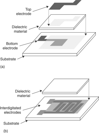
The faced plate geometry of Fig. 8.1(a) provides the largest capacitance at parity of electrode spacing and area, since it maximizes surface overlap. It also offers electromagnetic shielding due to the ‘closed’ configuration. The alternative option is an ‘open’ configuration based on coplanar electrodes interacting by means of fringing fields, as shown in Fig. 8.1(b). Also, the basic coplanar electrode pair can be replicated in the interdigitated (IDT) structure of Fig. 8.1(c), which results in the interdigitated capacitor (IDC).
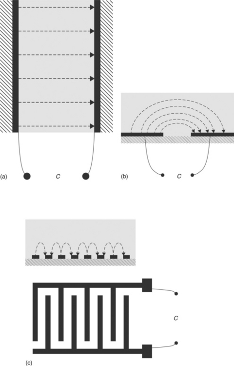
8.1 Configurations of capacitive sensors: (a) faced electrodes in a planar plate capacitor; (b) coplanar electrodes; (c) interdigitated electrodes.
In the following, the attention is focused on sensors implemented in TFT, i.e. applying screen printing or closely related processes stemmed therefrom (Prudenziati, 1994; White and Turner, 1997).
The configuration of Fig. 8.1(a) can be implemented in multilayer structures on a single side of the substrate with conductive films separated by dielectric layers in a stacked arrangement. When air, or another fluid, is the dielectric medium, the supporting solid surface for the top electrode is missing: therefore an additional substrate becomes necessary to host the top electrode, such as in diaphragm pressure sensors. This can be typically obtained by assembling plane substrates in combination with spacing layers or frames to create suspended configurations or laterally supported arrangements.
This result can be directly accomplished in LTCC technology, where ceramic green tapes are shaped, provided with necessary screen-printed films, stacked, laminated and co-fired at 800–900 °C (Golonka, 2006). Moreover, LTCC combined with standard TFT and silicon micromachining have introduced a hybrid or heterogeneous integration (Gongora-Rubio et al., 2001). In the field of sensor implementation, a particularly appreciable variety of three-dimensional (3D) microstructures is achievable with LTCC technology by means of vias and cavities created in the multilayer stack. Mechanical punching or laser scribing are typically used to form vias, cavities and cutouts in the individual green sheets before lamination and co-firing (Peterson et al., 2005).
When the thicknesses of commercially available green tapes of LTCC are a limitation for the design of feature sizes, including cavity airgap distance and diaphragm thickness of capacitive sensors, a viable option is to accomplish accurately designed structures by means of sacrificial layers. For instance, a layer of carbon-based paste can be printed to act as stable mechanical support for a subsequently printed electrode. During the next firing process, the carbon-based layer is burnt out, thereby releasing the active layer from the substrate and leaving it partially self-supported (Lucat et al., 2008). Other ‘fugitive phases’ and sacrificial volume materials (SVM) which create temporary inserts can be deposited and thermally removed to create freely-supported beams, plates and bridges (Gongora-Rubio et al., 2001; Peterson et al., 2005). Otherwise a screen-printed metal film is co-fired with the desired structure and chemically etched away, in the post-firing process, with a strong acid solution (Sippola and Ahn, 2006) or, similarly, a strontium-carbonate layer is applied which can be removed with a weak acid solution (Lucat et al., 2008).
Coplanar and IDT electrodes represented in Fig. 8.1(b,c) provide the most straightforward means to create capacitive sensors on a single side of the substrate. Substrates may be the most traditional rigid or flexible materials, ceramics or polymers (Prudenziati, 1994), but also increasing interest is addressed to new unconventional materials, such as paper, plastics and textiles. Representative examples are IDT capacitors and other patterned components screen-printed on fabrics, whose feasibility was recently demonstrated for applications in functional clothes with embedded sensors (Kim et al., 2010) and in instrumented textiles for healthcare applications (Kang et al., 2006).
8.4 Capacitive sensing based on geometrical variations
With reference to the sufficiently general case described by Eqs. [8.1] and [8.2], the geometrical parameters influencing capacitance are the armature gap g and overlap area A. Therefore, any physico–chemical quantity, e.g. pressure, force or acceleration, acting on capacitor plates to vary g or A is potentially measured with a capacitive sensor. Three cases will be illustrated in the following, where, respectively, g, A or both vary under the measurand action.
8.4.1 Sensing relying on changes of distance
Let us suppose that a parallel plate capacitor, as shown in the inset of Fig. 8.2, has initial gap g0 and capacitance C0. When one plate is rigidly moved and the gap is changed to g, the capacitance as a function of the gap C(g) can be conveniently expressed as the normalized capacitance C(g)/C(g0) = C(g)/C0 = c(x), where x = g/g0. It follows that c(x) = 1/x and the normalized sensitivity can be defined as k(x) = dc/dx resulting in k(x) = − 1/x2. Furthermore, the normalized nonlinearity, i.e. the departure from a constant-sensitivity value, defined as dk(x)/dx, will be dk(x)/dx = 2/x3.
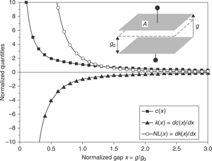
8.2 Normalized capacitance c, sensitivity k and nonlinearity NL as a function of the normalized gap size x = g/g0 for a parallel plate capacitor as shown in the inset.
The plots of these quantities, given in Fig. 8.2, make evident the advantage of a narrow gap in obtaining high sensitivity, but at the expense of a large nonlinearity. On the contrary, wide gaps improve linearity but reduce sensitivity and also result in a decrease of capacitance, which can be therefore swamped by parasitic effects in practical cases. Moreover, if the initial spacing g0 is set too small, a reduced span for the plate displacement remains possible before the plates touch each other, thus limiting the measurement range. The choice of g0 will necessarily be a trade off among the different requirements.
If the gap g itself is the measurand, i.e. the sensor is applied to measure distance or displacement, then a linear output can be attained by an electronic readout, which provides an output signal directly proportional to the sensor impedance |ZC|. Since |ZC| = 1/ω C, the output signal will be proportional to g at a given angular frequency ω. Alternatively, the capacitor can be inserted into a relaxation oscillator circuit whose frequency, proportional to the sensor capacitance, is taken as the output signal. A further limitation to linearity comes from the fringing effect caused by the electric field lines diverting from being parallel at the edge of the sensor electrodes due to their finite dimension. To counteract this effect, properly driven guard electrodes can be adopted to steer the electric field as parallel as possible between the sensor electrodes (Baxter, 1996).
With bending plates, such as diaphragms in pressure sensors, the spacing g, or equivalently the plate deflection z, is a function of position on the plate. For example, the deflection z of a disc diaphragm (inset of Fig. 8.3) having thickness t and radius R, rigidly clamped at the edge, for z < < t, is given by (Taroni, 1994):
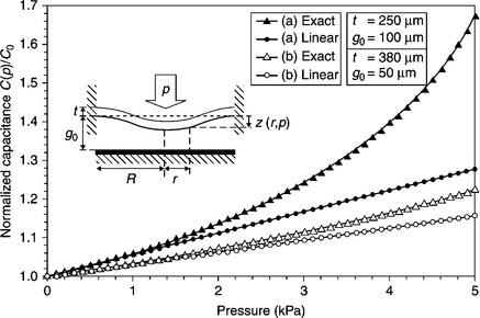
8.3 Normalized capacitance versus applied pressure for a deformable diaphragm sensor as shown in the inset; data calculated for E = 330 GPa (alumina), R = 7.5 mm and different values of diaphragm thickness t and gap g0. Exact and linearized plots refer to Eqs. (8.4) and (8.6), respectively.
where p is the uniform pressure applied to the disc, r is the radial distance from the center, ν and E are the Poisson’s ratio and Young’s modulus of the diaphragm material, respectively.
Therefore, the transduction function of a capacitive pressure sensor formed by a pair of electrodes placed respectively on a bending circular diaphragm and a faced rigid plane is:
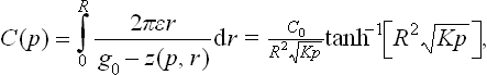
where ε = ε0εr is the permittivity of the dielectric medium, with ε ≈ ε0 in case of air, and:
For small deflections so that z/g0 < < 1, Eq. [8.4] can be approximated as in Taroni (1994):
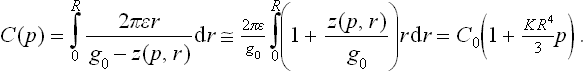
With a diaphragm homogeneous in thickness and composition, the maximum deflection zmax occurs at the centre (r = 0) and is constrained to be zmax(0) ≤ g0. Accordingly, the allowed full-scale pressure pmax, in deflection mode, is:
provided that it would not cause the flexural strength limit of the material σlim to be exceeded, in which case the full scale is bounded by the limit pressure plim ≅ 4t2σlim/(3R2).
Equations [8.4] to [8.6] show that the transduction characteristic C(p) becomes notably nonlinear at increasing pressures, but a proper design, with careful choice of g0, t and R of the diaphragm and of its elastic properties, together with operating the sensor in the lower part of the pressure range, can mitigate this effect. The plots of C(p)/C0 versus p are shown in Fig. 8.3 for a sensor with an alumina circular diaphragm as the results of computations for two different values of thickness t and gap g0. The exact and linearized expressions of Eqs. [8.4] and [8.6], respectively, are compared in the plots, showing that the 250 μm thick diaphragm provides higher sensitivity but larger nonlinearity. A marked improvement in linearity at parity of pressure is obtained for the 380 μm thick diaphragm, but in this case the gap g0 has been reduced from 100 μm to 50 μm in order to counteract, at least partially, the decrease in sensitivity caused by the thicker diaphragm.
An improvement in linearity with respect to uniform-thickness diaphragms could be achieved with bossed diaphragms, e.g. a disk thicker in the central portion to increase its rigidity there, or diaphragms provided with corrugations around the edge to increase the compliance there, which flatten the deflection profile and enable larger displacements. Both expedients, however, require tri-dimensional shaping, which is easier in silicon micromachining than in TFT.
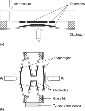
In practical implementations of capacitive pressure sensors, often an additional electrode (3) is placed around the edge of the sensing electrode (2) of C(p), resulting in the three-electrode configuration shown in Fig. 8.4. The additional electrode (3) and the electrode (1) on the faced plate form a reference capacitor Cref which is essentially unaffected by the applied pressure because of the negligible diaphragm deflection in the edge region. Both C(p) and Cref are equally sensitive to perturbing factors such as thermal effects and environmental changes. Therefore, the three-electrode configuration can be applied to compensate for interfering factors if the ratio C(p)/Cref is measured. Similar compensation effects are accomplished in differential capacitive pressure sensors.
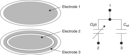
8.4 Three-electrode configuration for capacitive pressure sensor: the capacitance C(p) between electrodes 1 and 2 is sensitive to pressure, the capacitance Cref between electrodes 1 and 3 is virtually unaffected by pressure and can be used as a reference for compensation of permittivity variations and thermal effects.
8.4.2 Sensing relying on changes of area
Sensors in which the measurand changes the overlapping area A between electrodes benefit from the linear dependence of capacitance C versus A, provided that stray capacitances due to fringing effects are negligible.
This can be obtained if faced electrodes are made to displace relative to each other in the direction parallel to their surface while keeping the separation gap constant, resulting in a capacitance variation proportional to displacement. This characteristic has been applied for instance in the design of a capacitive torque sensor based on changes in area of two faced serrated teeth (Turner, 1989).
The variable-area principle can also be exploited in bending diaphragm capacitive pressure sensors. By applying a pressure p higher than the pressure pmax at which the diaphragm touches the bottom plate, capacitive pressure sensors can be operated in contact mode. The pressure causes increasingly larger regions of the diaphragm to touch (contact) the lower plate; therefore, provided that the electrode surfaces are electrically insulated, the capacitance is nearly proportional to the contact area, which in turn exhibits good linearity with respect to the applied pressure. This holds true over a wide range of pressures. However, this linearity comes at the expense of decreased sensitivity with respect to the deflection mode (Eaton and Smith, 1997).
8.4.3 Sensing relying on deformation
Both the distance and overlap area of electrodes can vary in a capacitive sensor when the measurand acts on the sensor volume in such a way to cause deformation. An example is shown in Fig. 8.5, where a planar capacitor formed by a dielectric film sandwiched between two conductor layers deforms under the effect of a longitudinal strain S = dl/l applied normal to the lateral surface. This structure works as a capacitive strain gauge, where strain induces a variation of capacitance through changes in dimensions due to stretching.
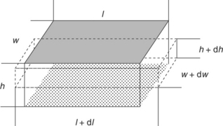
8.5 Capacitive strain gauge with strain applied along the length l normal to the top and bottom electrode faces causing longitudinal stretching and transverse contraction.
Assuming that the conductor films have negligible thickness, the fractional capacitance variation is:
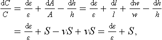
where ν is the Poisson’s ratio of the dielectric medium. The gauge factor GF, defined as GF = (dC/C)/S, is then:
The unity term comes from geometrical factors, while the second term accounts for the strain dependency of the dielectric permittivity and it is sometimes referred to as the ‘piezocapacitive’ effect in analogy with the corresponding effect in piezoresistors. A different configuration based on IDT electrodes can be used. The operating principle is similar but, in this case, closed form expressions for the capacitance variation and gauge factor are more complex to derive.
8.5 Capacitive sensing based on permittivity variations
Capacitive sensing of physical and chemical quantities, such as temperature, gas concentration, relative humidity as well as biosensors, frequently rely on changes in the dielectric permittivity of fluids or solid media. Also mechanical effects such as a pressure applied over the surface area of planar capacitors can produce capacitance variations related to permittivity changes (Arshak, K. et al., 2005).
The majority of capacitive sensors in chemical and bio-chemical applications have the open electrode configuration of Fig. 8.1(c) with coplanar IDT electrodes covered by the dielectric medium made by a bio-chemically-sensitive film facing the environment for maximum interaction. Optimization of the system requires the choice of the best dielectric film for sensing the target species together with the optimal choice of electrode configuration.
A rather general analysis of planar IDT capacitive sensors can be made with reference to the simplified three-medium model illustrated in Fig. 8.6; the model comprises the sensed medium (1), the substrate (2) and the inter-electrode space (3), each medium i with its dielectric permittivity εi, while the electrodes are assumed to be perfect conductors (Endres and Drost, 1991).
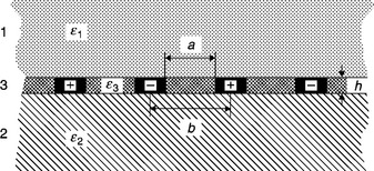
8.6 Three-medium model for an IDT capacitor after Endres and Drost (1991).
Neglecting edge effects, the sensor capacitance C can be computed from the capacitance per unit length CUC of a two-dimensional cell formed by an electrode pair, yielding:
where N and L are the number and length of the finger electrodes, respectively.
The capacitance of the unit cell CUC is given by the approximated expression:
where a, b and h are the finger spacing width, distance (pitch) and thickness, respectively. K[x] is the complete elliptic integral of the first kind (Bronshtein et al., 2007), given by:
and C1 and C2 are the contributions of the upper medium and substrate permittivities, and C3 that of the inter-electrode film. If the medium 3 is a single overlaying film that entirely buries the IDT electrodes, as it often happens with TFT sensors, then ε3 = ε1 in Eq. [8.11].
An expression slightly different from Eq. [8.11], yet substantially equivalent, was presented for capacitive humidity sensors in Smetana and Wiedermann (1987). A review of IDT sensors and transducers is given in Mamishev et al., (2004).
8.6 Examples of devices and their applications
Several studies have been carried out on design and implementation methods of thick-film capacitive pressure sensors. With respect to the more usual piezoresistive devices, capacitive sensors call for less extensive processing, are less susceptible to misalignment errors and are potentially more stable at high temperature. On the other hand, a much closer control of inter-electrode distance is mandatory in design and manufacture of capacitive devices for reproducible behaviour.
The cross-section of the differential capacitance pressure sensor described in Dargie and Hughes (1994) is shown in Fig. 8.7.
8.7 Cross-section of a thick-film capacitive differential pressure sensor after Dargie and Hughes (1994).
It represents a successful application of traditional TFT methods and materials. The circular alumina diaphragm (250 μm thickness and 15 mm diameter) with electrodes on its upper and lower surfaces is sandwiched between two outer fixed plates forming top (T) and bottom (B) electrodes. The electrodes on the three plates together give rise to two capacitances CT and CB that, under applied pressure, vary in an opposite way in a push–pull operation. The outer electrodes are driven with anti-phase voltage signals so that the voltage between the inner electrodes and ground depends on the normalized capacitance difference (CT – CB)/(CT + CB). This ensures good common-mode rejection of unwanted signals due to changes in temperature and dielectric constant, while it also improves linearity due to partial compensation between the nonlinearities of CT and CB. The measured sensitivity was 0.63 mV kPa− 1 with a nonlinearity lower than 3% FS (full scale) over the pressure range 0 ÷ 207 kPa (0 ÷ 30 psi).
The co-design of a peculiar electrode shape and a tailored frequency–output electronic interface were described in Crescini et al. (1997) for a capacitive pressure sensor that exhibits a linearity error lower than 2% FS over an extended pressure range (0 ÷ 600 kPa), with a sensitivity of 12 Hz kPa− 1 and the output virtually independent of the power supply. As shown in Fig. 8.8(a), the sensor applies screen-printed electrodes on circular alumina plates, one of which is a fixed substrate, while the other is a 500 μm thick diaphragm that deflects under applied pressure p. While the substrate electrode is circular, the diaphragm electrode has a specific spiral shaping that is surrounded by a guard electrode. As shown Fig. 8.8(b), the sensor is connected to an electronic circuit based on a relaxation oscillator which interfaces to the sensor capacitance C, drives the guard electrode and outputs a square-wave signal whose frequency f is proportional to 1/C(p). The combination of the electrode shaping and the capacitance to frequency conversion optimizes linearity of the overall pressure-to-frequency transduction function.
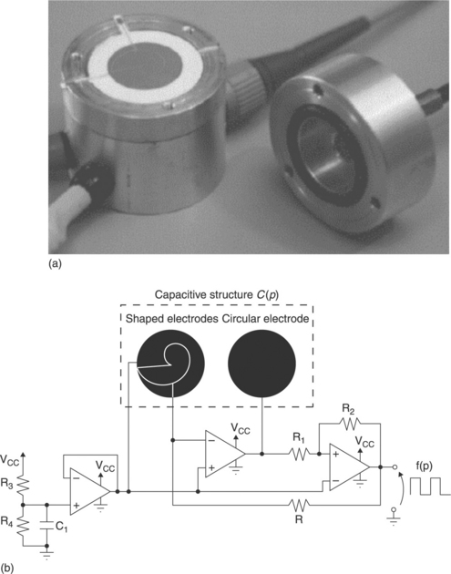
8.8 Capacitive pressure sensor with improved linearity after Crescini et al. (1997): (a) view of the sensor with shaped electrode; (b) signal conditioning electronic circuit for conversion from capacitance to frequency output.
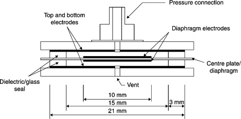
Capacitive pressure sensors in standard thick-film technology are manufactured, among others, by Endress + Hauser (www.endress.com) and Kavlico (www.kavlico.com). Endress + Hauser offers a gauge sensor that takes advantage of the three-electrode configuration illustrated in Fig. 8.4, as well as a differential pressure sensor, as shown in Fig. 8.9(a, b), respectively. Kavliko manufactures the capsule shown in Fig. 8.10, available either as a gauge or absolute pressure sensor, with the hybrid signal-conditioning electronics fitted behind the diaphragm.
8.9 Schematic view of ceramic capacitive pressure sensors manufactured by Endress + Hauser: (a) gauge pressure sensor, model Cerabar PMC71 adapted from Endress + Hauser A; (b) differential pressure sensor, models Deltabar PMD70 and FMD76, adapted from Endress + Hauser B.

8.10 Ceramic capacitive pressure sensor manufactured by Kavlico, model PS312 adapted from Kavlico: (a) view of the arrangement where the hybrid electronic circuit is fitted behind the sensing diaphragm 33 mm in diameter; (b) picture of the sensor capsule.
A capacitive pressure microsensor was recently described in Sippola and Ahn (2006). This device applies thick-film electrodes separated by a thin airgap created by a sacrificial layer process, resulting in a hybrid micro-fabrication technique. The structure and fabrication steps of the sensor are shown in Fig. 8.11: a bottom gold electrode is printed on 96% alumina into which vias have been previously drilled by laser to create access to Au-based thick-film paste and permit chemical etchant penetration. The electrode is protected by a dielectric film over which the sacrificial layer made by a gold film is screen-printed. A top protection dielectric and electrode replicate the bottom structure. A backside-sealing layer completes the fabrication. Sacrificial layer thicknesses of 12 and 22 μm were used to create two different cavity airgap distances, resulting in the capacitance at zero gauge pressure of about 8 and 6 pF, respectively. The sensor was intended for high temperature and a harsh environment, and showed hermeticity up to 500 °C. In the characterization up to 300 °C in a pressure range of 0 to 345 kPa, the average sensitivity for the sensor with a 12 μm airgap was 1.3 fF kPa− 1. The temperature coefficient of capacitance (TCC) was 97 ppm °C− 1 over the temperature range of 25 to 300 °C.

8.11 Ceramic capacitive pressure sensor after Sippola and Ahn (2006); the fabrication steps for achieving the cavity are: (a) laser drilling of vias; (b) screen-printing of bottom electrode; (c) screen-printing of bottom dielectric layer; (d) screen-printing of sacrificial layer; (e) screen-printing of top dielectric diaphragm and top electrode; (f) etching of sacrificial layer and screen-printing of backside sealing dielectric.
Capacitive pressure sensors using thick-film and LTCC technologies have been reported in Belavič et al. (2008), Fonseca et al. (2002), Meijerink et al. (2005), Plumlee et al. (2002), Radosavljević et al. (2009) and Tamas et al. (2010).
Particularly relevant is the design described in Fonseca et al. (2002), which implemented concepts developed by English and Allen (1999) for a capacitive pressure sensor with wireless readout for high-temperature applications. The sensor consists in a sealed cavity; its top side supports a passive LC resonator comprised of a movable diaphragm capacitor and a fixed inductor, as shown in Fig. 8.12, thereby causing the sensor resonant frequency of around 18 MHz to be dependent on pressure. The sensor signal is read by an external loop antenna. The passive nature of the sensor removes the need for on-board electronics, power supply, or contacts to withstand high operating temperature up to 400 °C. In a pressure range from 0 to around 700 kPa the average sensitivity was 1.41 Hz kPa− 1.
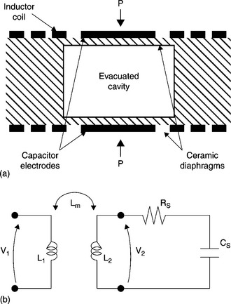
8.12 Capacitive absolute pressure sensor with contactless readout for high-temperature applications after Fonseca et al. (2002): (a) schematic view of the sensor structure with sensing capacitor and integrated inductor coil on ceramics; (b) equivalent circuit of the resulting LC resonator and external loop antenna for readout.
A thick-film capacitive sensor as a part of a resonant circuit, excited by means of induction coupling across an air-gap, had been already successfully implemented by Turner (1989) for a contactless shaft torque sensor for automotive applications (Turner and Austin, 2000). The realization comprised two unusual technological features: the use of printing process on curved surfaces and application of dielectric and conductive inks curable at low temperature on steel. Either the change in the resonance frequency of the circuit or the change in reflected impedance measured at the exciting coil could be taken as the response signal for the torque measurement.
Capacitive strain sensors based on TFT have been studied (Arshak, K. et al., 2005; Arshak et al., 2000) in both sandwich and planar configurations that are illustrated in Figs. 8.13(a) and 8.13(b), respectively. In the former case, two types of dielectric were used: lead zirconate titanate (PZT) and polyvinylidene fluoride (PVDF). PZT offers higher permittivity than PVDF. Sensors, tested in the range 0–350 με over the frequency range 1–100 kHz, have shown that PZT-based capacitors provide higher gauge factor of 6 as compared to 3.5 for PVDF-based capacitors, but higher TCC of around 4000 ppm °C− 1 instead of 2500 ppm °C− 1 for PVDF at 25 °C. Both strain sensors showed low values of dissipation factor but the gauge factor of the PZT-based sensor was frequency-dependent.
8.13 Configurations of capacitive strain sensors: (a) planar sandwich structure; (b) interdigitated structure.
The comparison between planar sandwich and IDC configurations for strain sensors was reported in Arshak, K. et al., (2005) on samples prepared with a blend of TiO2 powder in a polymeric binder. The screen-printed capacitors were cured at 120 °C. Ag-based conducting electrodes and a glass substrate were the other parts of the sensors. They were tested under strains up to beyond 300 με. Gauge factors of 5 and 30 were recorded for interdigitated and sandwich capacitors, respectively. The higher sensitivity of the sandwich-type device was ascribed to the larger contribution of the geometrical factor. However, the sandwich sensor suffered from hysteresis and repeatability errors (7 and 18% FS, respectively) of about an order of magnitude higher than those of the IDT-type sensor. The formulated dielectric paste resulted in a TCC of about 1000 ppm/°C at room temperature for both the sandwich and IDT sensors, with a marked increase with increasing temperature.
Interdigitated capacitive strain gauges that can be integrated directly onto engineering components fabricated using direct-write thermal spray (DWTS) and intended for operation in harsh environments over an extended temperature range have been described by Li et al. (2007). Sensor elements were fabricated on polyethylene, etherester amide (EEA), graphite composite, fibreglass reinforced epoxy (FR4) composite, and alumina substrates. Gauge factors ranging from 0.9 to 20 have been measured, and the gauge factor was found to depend strongly on the underlying substrate material.
A proper selection of the dielectric material and the sensor design enabled the construction of a miniature frequency-output thick-film temperature sensor proposed in Leppävuori et al. (1983). The selected dielectric is a SrTi03-BaTi03 solid solution, whose composition determines the transition to paraelectric behaviour at Tc = − 47 °C; therefore its permittivity is a linear decreasing function of temperature at T > Tc, according to the Curie–Weiss law. The sensor is a planar sandwich capacitor whose capacitance varied from about 1000 to 100 pF in the range from − 30 to + 80 °C, with a sensitivity of 1.3% °C− 1 at 25 °C, while the spread across the batch was as low as 0.02% °C− 1. When the sensor was coupled to a complementary metal-oxide-semiconductor (CMOS) oscillator, an output frequency was obtained linearly increasing with temperature from − 25 to 85 °C, with a sensitivity of 20 Hz °C− 1 and a linearity error of 0.4 °C.
Capacitive IDT thick-film sensors for the measurement of humidity have been known for a long time. They were proposed for instance in Smetana and Wiedermann, (1987), where the permeation and adsorption of water in various dielectric thick-film compositions were studied, and even earlier in Lucas et al. (1976) for the measurement of moisture content in soil.
An interesting structure of thick-film capacitive relative humidity (RH) sensors is a hybrid between the sandwich and IDT configurations described in Qu and Meyer (1997). The idea is to compensate for the rather slow response of the highly sensitive sandwich humidity sensors with the much faster response of IDT sensors, which, however, are typically less sensitive. Fig. 8.14 shows the hybrid structure designed to implement this approach. A 40 μm porous MnWO4 ceramic layer is sandwiched between two 10 μm polarity-reversed, IDT Pt films. A negative temperature cuefficient (NTC) thick-film sensor to compensate for thermal effects and a Pt refresh heater on the back-side of the alumina substrate complete the device. Variations of capacitance and resistance over three orders of magnitude were observed in the range from 25 to 95% RH with a response time of 10 s.
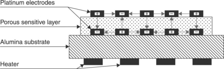
8.14 Structure of thick-film capacitive humidity sensor after Qu and Meyer (1997); the design is a hybrid between the sandwich and IDT configurations.
Innovative solutions under study include ink-jet-printed capacitive humidity sensor tags for passive RFID systems (Virtanen et al., 2011) and screen-printed films using multiwall carbon nanotube and SiO2 powders (Chen et al., 2009).
Raindrops can be sensed by capacitive methods implemented in TFT. A capacitive rain sensor based on silver-based polymeric paste screen-printed on sodocalcic glass and cured at 120 °C was presented in Bord et al. (2006). There is no sensitive dielectric layer in the capacitor, therefore potential problems of reliability and stability due to dielectric poisoning and ageing are circumvented. The sensor is made of three protected coplanar electrodes that define a differential configuration with a sensitive element with capacitance C1 affected by water, and a reference element with capacitance C2. In dry conditions, C1 = C2, whereas an imbalance between C1 and C2 reveals the presence of water on the sensor; the sensor time response is negligible, making real-time monitoring achievable.
A commercially available ceramic capacitive rain sensor produced by Telecontrolli (www.telecontrolli.com) is shown in Fig. 8.15. The sensor has IDT electrodes on one side of the alumina substrate, while a refresh resistive heater and a temperature sensor are placed on the opposite side.
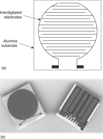
8.15 Ceramic capacitive rain sensor available from Telecontrolli adapted from Telecontrolli: (a) schematic view of the interdigitated sensor structure on alumina substrate; (b) picture of the sensor seen from top and bottom faces.
As an extension of capacitive sensing, discrimination among the various possible contributions (physi-sorption, chemi-sorption, condensation in pores, etc.) of dielectric media to the response of RH sensors can benefit from impedance spectroscopy, through the study of the complex impedance spectra collected in various environmental conditions. Examples of such studies have been reported for a sensor consisting in TiO2-based ink spin-coated on top of IDT electrodes on alumina (Faia et al., 2004) and a 20 nm grain-size ZrO2-based ink screen-printed on gold IDT electrodes deposited on a silicon substrate (Wang et al., 2009). Similar impedance-spectroscopy investigations are well known in the field of chemical gas sensors (Malagù et al., 2005) and bio-sensors (Lucarelli et al., 2005). Each of these application fields is a wide and diverse sector by itself (Galán-Vidal et al., 1995) and will not be covered here.
A further wide field of hybridization of technologies on one side and capacitive sensors on the other side is represented by μTAS (micro total analysis systems) and LabOnChip systems for biochemical applications, one specific sector being that of microfluidics. Special emphasis is posed in developing efficient and cost-effective methods and technologies to provide microfluidic systems with embedded actuating and sensing capabilities. An important role in this scenario is played by TFT and LTCC (Golonka, 2006; Peterson et al., 2005), due to their flexibility and typical feature sizes compatible with the required dimensions of microfluidic systems.
One example of these opportunities is the device described in Demori et al. (2011), which combines PDMS (polydimethylsiloxane) soft photolithography and screen-printing techniques. The device goal is to discriminate and characterize fluids in a microchannel on the basis of their dielectric permittivity. Fig. 8.16 shows the device structure formed by the microchannel with three pairs of electrodes screen-printed alongside from an Ag polymeric ink (DuPont 5000) and buried into the PDMS on a glass substrate. The microchannel is thus placed in the fringe field of the electrodes. The inner electrode pair work as a sensing capacitor while the two outer pairs act as guarding sections. The sensing capacitance is around 80 fF with a variation of few per cent between air and water in the microchannel. A tailored electronic interface system has been developed that drives the sensing and guard capacitors with a sinusoidal voltage signal and reads the sensor current with a synchronous detection technique to obtain bandwidth narrowing and improve the signal-to-noise ratio. A capacitance resolution of 0.06 fF is obtained over a bandwidth of 10 Hz. The sensor is able to distinguish clearly between continuous water flow and air–water segmented flow in the microchannel. In terms of capacitance, the air-filled and water-filled conditions differ by about 10 fF. The ability to reliably discriminate between various fluids with different permittivities has been demonstrated, as shown in Fig. 8.17.
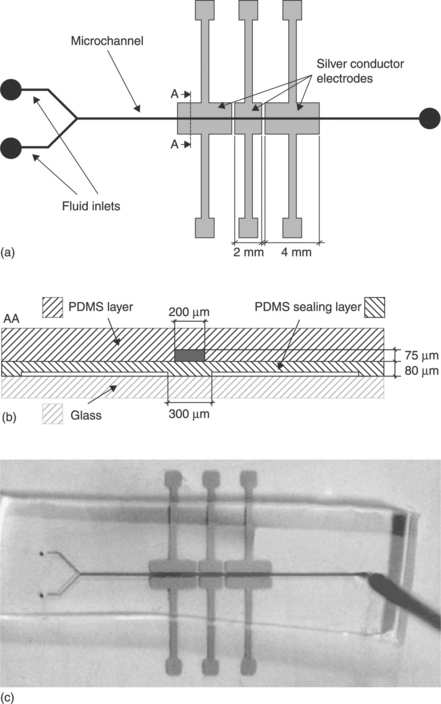
8.16 Screen-printed capacitive sensor embedded into a microfludic device after Demori et al. (2011): (a) top view with microchannel and electrodes; (b) cross-section; (c) device picture where a liquid is visible in the microchannel.
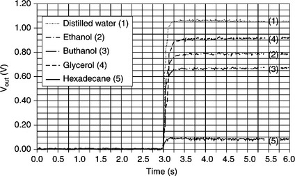
8.17 Measured output signal versus time of the capacitive sensor system of Fig. 8.16 due to step injections of fluids with different dielectric permittivity. The signal traces are superimposed in time for better comparison.
8.7 Conclusion and future trends
Capacitive sensors relying on geometrical variations can in general be considered mature devices, though continuing developments will most likely take place in new designs. For measuring mechanical quantities, capacitive sensors, together with piezoresistive sensors, are expected to remain among the prevalent technologies in the near future (AMA, 2010). Capacitive thick-film sensors will in many cases evolve towards miniaturization through a convergence of different technologies like LTCC and microfabrication, such as in the devices described in Belavič et al. (2008), Meijerink et al. (2005) and Sippola and Ahn (2006).
Ceramic-based capacitive sensors will further develop their ability to operate in hostile environments, such as over extended temperature ranges. Improvements can be expected in coupling capacitive sensors with tailored electronic circuits, which are increasingly capable of ensuring high accuracy with small capacitance values and variations. This, combined with suitable signal processing techniques as allowed by new-generation processors, will result in increased performance and functionality, yet reduced power consumption.
Capacitive sensors relying on permittivity changes will most likely experience significant expansion. Especially for chemical sensing, they are expected to take advantage of material developments and processing technologies.
Capacitive sensors on plastic and flexible substrates are attracting increasing attention to reduce cost and develop, for instance, smart labels or multi-sensor devices for environmental monitoring such as in Oprea et al. (2009) and Courbat et al. (2009). Printed-film technologies, though not necessarily screen-printing, have the potential to play a significant role in this rapidly-evolving scenario.
Also based on the variable-permittivity principle are capacitive touch sensors. They represent a field where significant expansions are expected. Capacitive touch sensors are gradually replacing mechanical switches and buttons in a wealth of applications due to their superior aesthetics, flexibility and reliability. Capacitive sensors also enable sliders, trackpads and, thereof, advanced human–machine-interface components and functions. Additionally, capacitive sensors are used for proximity sensing where no contact is required between the sensor and the target, without line-of-sight constraints. This in turn opens other possibilities, such as fluid level measurement. Important markets exist, such as the consumer and automotive sectors, and dedicated integrated circuits are increasingly available from semiconductor manufacturers, which is contributing to the penetration of the capacitive technology (Arora and Verma, 2010). Here, there is room for research and development on printed-film capacitive sensors, which can offer flexibility in design, materials and configurations, and low cost even at medium production volumes.
8.8 Sources of further information
• IEEE Instrumentation and Measurement Society (IMS) Society dedicated to research concerning the theory, methodology and practice of measurement, and in the design, development and evaluation of instrumentation and associated measurement systems (http://www.ieee-ims.org).
• IEEE Sensors Council Council dedicated to research on the theory, design, fabrication, manufacturing and application of devices for sensing and transducing physical, chemical, and biological phenomena, with emphasis on the electronics, physics and reliability aspects of sensors and integrated sensor-actuators (http://www.ieee-sensors.org).
• International Microelectronics and Packaging Society (IMAPS) Society dedicated to the advancement and growth of microelectronics and electronics packaging technologies through professional education (http://www.imaps.org/default.asp).
8.9 References
AMA Sensor Trends 2014: Trends in Future-Oriented Sensor Technologies. Association for Sensor Technology, Berlin, Germany, 2010. Available from. http://www.ama-sensorik.de
Arora, P., Verma, M., Emerging trends in automotive capacitive touch-sensing. Electronic Products. 2010 November 2010. Available from. http://www2.electronicproducts.com
Arshak, A., Arshak, K., Morris, D., Korostynska, O., Jafer, E. Investigation of TiO2 thick-film capacitors for use as strain gauge sensors. Sensors and Actuators A. 2005; 122:242–249.
Arshak, K.J., McDonagh, D., Durcan, M.A. Development of new capacitive strain sensors based on thick-film polymer and cermet technologies. Sensors and Actuators A. 2000; 79:102–114.
Arshak, K., Jafer, E., Fox, A. Design of a new thick-film capacitive pressure and circuitry interface. Composites Science and Technology. 2005; 65:757–764.
Baxter, L. Capacitive Sensors: Design and Applications. New York: Wiley-IEEE Press; 1996.
Belavič, D., Zarnik, M.S., Macek, S., Jerlah, M., Hrovat, M., et al, Capacitive pressure sensors realized with LTCC technology. International Spring Seminar on Electronics Technology, 2008. ISSE’08, Budapest, May 7–11. 2008:269–272.
Bord, I., Tardy, P., Menil, F. Influence of the electrodes configuration on a differential capacitive rain sensor performances. Sensors and Actuators B. 2006; 114:640–645.
Bronshtein, I.N., Semendyayev, K.A., Musiol, G., Muehlig, H. Handbook of Mathematics. Berlin Heidelberg: Springer-Verlag; 2007.
Chen, W.P., Zhao, Z.G., Liu, X.W., Zhang, Z.X., Suo, C.G. A capacitive humidity sensor based on multi-wall carbon nanotubes (MWCNTs). Sensors. 2009; 9:7431–7444.
Courbat, J., Briand, D., Oprea, A., Bârsan, N., Weimar, U., et al. Multi sensor platform on plastic foil for environmental monitoring. Procedia Chemistry. 2009; 1:597–600.
Crescini, D., Ferrari, V., Marioli, D., Taroni, A. A thick-film capacitive pressure sensor with improved linearity due to electrode shaping and frequency conversion. Measurement Science and Technology. 1997; 8:71–77.
Dargie, P.G., Hughes, S.T. A thick-film capacitive pressure transducer. Measurement Science and Technology. 1994; 5:1216–1220.
Demori, M., Ferrari, V., Poesio, P., Strazza, D. A microfluidic capacitance sensor for fluid discrimination and characterization. Sensors and Actuators A. 2011; 172:212–219.
Eaton, W.P., Smith, J.H. Micromachined pressure sensors: review and recent developments. Smart Materials and Structures. 1997; 6:530–539.
Endres, H.E., Drost, S. Optimization of the geometry of gas-sensitive interdigital capacitors. Sensors and Actuators B. 1991; 4:95–98.
Endress + Hauser A, Technical Information Cerabar S PMC71, PMP71, PMP75, TI383PEN_0510.pdf. Available from: http://www.endress.com
Endress + Hauser B, Technical Information Deltabar S PMD70/75, FMD76/77/78, TI382PEN_0510.pdf. Available from: http://www.endress.com
English, J.M., Allen, M.G., Wireless micromachined ceramic pressure sensors. Proceedings of the 12th IEEE Microelectromechanical Systems Conference, Orlando, Florida, USA, 17–21 January. 1999. [pp. 511–516.].
Faia, P.M., Furtado, C.S., Ferreira, A.R. Humidity sensing properties of a thick-film titania prepared by a slow spinning process. Sensors and Actuators B. 2004; 101:183–190.
Fonseca, M.A., English, J.M., vonArx, M., Allen, M.G. Wireless micromachined ceramic pressure sensor for high-temperature applications. Journal of Micro-electromechanical Systems. 2002; 11:337–343.
Galán-Vidal, C.A., Muñoz, J., Domínguez, C., Alegret, S. Chemical sensors, biosensors and thick-film technology. Trends in Analytical Chemistry. 1995; 14:225–231.
Golonka, L.J. Technology and applications of low temperature cofired ceramic (LTCC) based sensors and microsystems. Bulletin of the Polish Academy of Sciences: Technical Sciences. 2006; 54:224–231.
Gongora-Rubio, M.R., Espinoza-Vallejos, P., Sola-Laguna, L., Santiago-Avilés, J.J. Overview of low temperature co-fired ceramics tape technology for meso-system technology (MsST). Sensors and Actuators A. 2001; 89:222–241.
Kang, T.H., Merritt, C., Karaguzel, B., Wilson, J., Franzon, P., et al, Sensors on textile substrates for home-based healthcare monitoring. Proceedings of the 1st Distributed Diagnosis and Home Healthcare (D2H2) Conference, Arlington, Virginia, USA, 2–4 April. 2006.
Kavlico, OEM Pressure Modules: Ceramic Capacitive – Gage and Absolute Pressures, OEM_Sensor_Modules.pdf. Available from: http://www.kavlico.com
Kim, Y., Kim, H., Yoo, H.J. Electrical characterization of screen-printed circuits on the Fabric. IEEE Transaction on Advanced Packaging. 2010; 33:196–205.
Leppävuori, S., Niemela, P., Piila, T., Uusimäki, A. Miniature frequency-output temperature transmitter based on a ceramic capacitive sensor. Sensors and Actuators. 1983; 4:573–580.
Li, J., Longtin, J.P., Tankiewicz, S., Gouldstone, A., Sampath, S. Interdigital capacitive strain gauges fabricated by direct-write thermal spray and ultrafast laser micromachining. Sensors and Actuators A. 2007; 133:1–8.
Lucarelli, F., Marrazza, G., Mascini, M. Enzyme-based impedimetric detection of PCR products using oligonucleotide-modified screen-printed gold electrodes. Biosensors and Bioelectronics. 2005; 20:2001–2009.
Lucas, M.S.P., Stephens, L.E., Dawess, W.H., Casey, M.R. Thick-film sensors for agricultural applications. Journal of Agricultural Engineering Research. 1976; 21:1–8.
Lucat, C., Ginet, P., Castille, C., Debéda, H., Ménil, F. Microsystems elements based on free-standing thick-films made with a new sacrificial layer process. Microelectronics Reliability. 2008; 48:872–875.
Malagù, C., Carotta, M.C., Gherardi, S., Guidi, V., Vendemmiati, B., et al. AC measurements and modeling of WO3 thick-film gas sensors. Sensors and Actuators B. 2005; 108:70–74.
Mamishev, A.V., Sundara-Rajan, K., Yang, F., Du, Y., Zahn, M. Interdigital Sensors and Transducers. Proceedings of the IEEE. 2004; 92:808–845.
Meijerink, M.G.H., Nieuwkoop, E., Veninga, E.P., Meuwissen, M.H.H., Tijdink, M.W.W.J. Capacitive pressure sensor in post-processing on LTCC substrates. Sensors and Actuators A. 2005; 123–124:234–239.
Oprea, A., Courbat, J., Bârsan, N., Briand, D., de Rooij, N.F., et al. Temperature, humidity and gas sensors integrated on plastic foil for low power applications. Sensors and Actuators B. 2009; 140:227–232.
Peterson, K.A., Patel, K.D., Ho, C.K., Rohde, S.B., Nordquist, C.D., et al. Novel microsystem applications with new techniques in low-temperature co-fired ceramics. International Journal of Applied Ceramic Technology. 2005; 2:345–363.
Plumlee, D.G., Morales, Y., Cheek, B., Paris, A.J., Ackler, H.A., et al, Pressure sensors built in low temperature co-fired ceramic materials. Proceedings of IMAPS Advanced Technology Workshop on Packaging of MEMS and Related Micro Integrated Nano Systems, Denver, Colorado, USA, September 6–8. 2002.
Prudenziati, M. Thick-Film Sensors. Amsterdam: Elsevier; 1994.
Puers, R. Capacitive sensors: when and how to use them. Sensors and Actuators A. 1993; 37–38:93–105.
Qu, W., Meyer, J.U. A novel thick-film ceramic humidity sensor. Sensors and Actuators B. 1997; 40:I75–I82.
Radosavljević, G.J., Živanov, L.D., Smetana, W., MarićA, M., Unger, M., et al. A wireless embedded resonant pressure sensor fabricated in the standard LTCC technology. IEEE Sensors Journal. 2009; 9(12):1956–1962.
Sippola, C.B., Ahn, C.H. A thick-film screen-printed ceramic capacitive pressure microsensor for high temperature applications. Journal of Micromechanics and Microengineering. 2006; 16:1086–1091.
Smetana, W., Wiedermann, W. Using integrated capacitive humidity sensors in thick-film technology. Sensors and Actuators. 1987; 11:329–337.
Tamas, C., Marghescu, C., Ionescu, C., Vasile, A., Implementing a capacitive pressure sensor realized on LTCC. Proceedings of SPIE. 2010:7821.
Taroni, A. Capacitive sensors. In: Prudenziati M., ed. Thick-Film Sensors. Amsterdam: Elsevier; 1994:245–258.
Telecontrolli, Rain Sensor, RAIN_SENSOR.pdf. Available from: http://www.telecontrolli.com
Turner, J.D. The development of a thick-film non-contact shaft torque sensor for automotive applications. Journal of Physics E: Scientific Instruments. 1989; 22:82–88.
Turner, J.D., Austin, L. Sensors for automotive telematics. Measurement Science and Technology. 2000; 11:58–79.
Virtanen, J., Ukkonen, L., Björninen, T., Elsherbeni, A.Z., Sydänheimo, L. Inkjet-printed humidity sensor for passive UHF RFID systems. IEEE Transactions On Instrumentation and Measurement. 2011; 60(8):2768–2777.
Wang, J., Su, M.Y., Qi, J.Q., Chang, L.Q. Sensitivity and complex impedance of nanometer zirconia thick-film humidity sensors. Sensors and Actuators B. 2009; 139:418–424.
White, N.M., Turner, J.D. Thick-film sensors: past, present and future. Measurement Science and Technology. 1997; 8:1–20.