
Laser-printed micro- and meso-scale power generating devices
Abstract:
This chapter describes how laser direct-write (LDW) processes can be applied to the rapid prototyping of micro- and meso-scale power sources. The chapter reviews the use of laser-induced forward transfer (LIFT) to deposit patterns of complex suspensions comprising the functional materials required for printing ultracapacitors, primary and secondary batteries and dye-sensitized solar cells (DSSC). The chapter describes the preparation of embedded microbatteries via LDW and concludes with a discussion on the present and future status of these laser-based digital microfabrication techniques.
18.1 Introduction
The trend for developing increasingly smaller and more autonomous microelectronic systems has not yet been matched by power sources with correspondingly reduced volumes. These microelectronic systems and devices have created a need for unique types of micro-power sources capable of delivering high energy densities within usually limited form factors. Furthermore, to be effective, the micro-power sources must be comprised of different components such as energy-harvesting elements for power generation, microbatteries for energy storage and electrochemical capacitors for activities requiring high power surges. Depending on the application and performance requirements, various combinations of these components might be required.
This need has gone unfulfilled due to the difficulties of depositing and processing at low temperatures complex materials for power generation and of building the required structures within limited form factors using traditional thin-film deposition techniques. Furthermore, standard lithography techniques involving multiple steps such as material deposition, lithographic masking and etching processes are not well suited for the fabrication of non-planar structures common in most power sources. As an alternative, non-lithographic processes known as direct-write techniques allow the printing of patterns of complex material systems onto virtually any type of surface to generate the required structures in digital fashion. The use of printing techniques such as laser direct-write (LDW) offer unique opportunities towards the development and customization of various types of micro-power sources such as electrochemical ultra-capacitors and die-sensitized solar cells, as well as primary and secondary embedded batteries. In this chapter, the use of laser-based direct-write techniques for printing intricate patterns of thick-film structures for the development of micro- and meso-power generating devices will be reviewed and the results obtained to date briefly described.
The application of laser printing or LDW techniques has grown steadily since the first reports of patterned copper deposition by laser forward transfer made by Bohandy and coworkers 25 years ago (Bohandy et al., 1986). These general techniques employ a pulsed laser to locally transfer material from a source film onto a substrate in close proximity to or in contact with the film. The source is typically a coated laser-transparent substrate, referred to as the target, donor substrate, or ribbon. Laser pulses propagate through the transparent ribbon until they are absorbed by the film. Above an incident laser energy threshold, material is ejected from the film and transferred toward the acceptor or receiving substrate. Such laser-induced forward transfer techniques, known as LIFT, belong to a class of laser-based direct-write processes capable of generating a high-resolution pattern without the need for lithogaphic processes afterwards. Other examples of LDW techniques include pyrolitic or photolytic decomposition of gas- or liquid-phase precursors, also known as laser chemical vapor deposition (CVD) or laser-assisted deposition (Herman, 1989; Osgood and Deutsch, 1985). However, these non-forward transfer techniques will not be discussed in this chapter because they are not suitable for printing the types of materials required for the fabrication of power sources.
Translation of the ribbon and receiving substrate, and/or scanning and modulating the laser beam enable complex pattern formation. Commercially available, computer-controlled translation stages or galvonometric scanning mirrors enable high-resolution patterns from the individually written 3D pixels or voxels resulting from the laser forward transfer process. Figure 18.1 shows a schematic illustrating the basic elements required for the LDW apparatus. Since the source of energy for the transfers, i.e. the laser, is decoupled from the material to be printed, very high writing speeds, in excess of meters per second, can be achieved. In practice, the printing speeds are limited by the firing rate of the laser and/or how fast the ribbon and the receiving substrate can be translated, although roll-to-roll processes are certainly compatible with LDW.

One may consider the LDW technique to be analogous to ink-jet deposition of functional materials without the constraints of a nozzle, and with the added benefits of laser processing, such as material modifications and micromachining. This added versatility in comparison to other printing methods enables LDW to find opportunities in fields ranging from metals to biological and soft condensed matter, and have been applied successfully to the printing of materials for power generation applications.
This chapter will provide a brief overview of the laser forward transfer and LDW literature, with a particular emphasis towards its application for the fabrication of micropower storage systems such as ultracapacitors and microbatteries, and energy -harvesting systems such as dye-sensitized solar cells (DSSC). The chapter concludes with a discussion of the role that the LDW technique may play in the future of microelectronic manufacturing and provides a glimpse of what the future of printed power sources might look like.
18.2 Background to laser-induced forward transfer (LIFT)
The laser forward transfer process was first used in depositing copper metal patterns inside a vacuum chamber (Bohandy et al., 1986). Excimer laser pulses (= 193 nm, 15 ns) were focused with a cylindrical lens to a 25 mm long by 50 μm wide line on a source substrate containing a thin copper film. The Cu was transferred to Si and fused silica substrates, where further examination revealed resistivities ranging between 3 to 50 times the value for bulk copper with adhesion behavior that passed the ‘tape test’. Bohandy’s group coined the term laser-induced forward transfer (LIFT) to denote the process and developed a model to describe how it worked. According to this model: (1) the laser pulse heats the interface of the film at the source substrate; (2) a resulting melt front propagates through the film until it reaches the free surface; (3) at about this time, the material at the interface is superheated beyond its boiling point until, (4) the resulting vapor-induced pressure at the interface propels the molten film forward towards the acceptor substrate (Adrian et al., 1987). The same group then demonstrated that this process can be carried out in air, i.e. under atmospheric conditions, without the need for a vacuum (Bohandy et al., 1988).
The LIFT technique is simple and can be used with a wide variety of film materials, mainly metals such as Cu and Ag (Bohandy et al., 1988), Al (Schultze and Wagner, 1991), W (Tóth et al., 1993; Kántor et al., 1994) and Cr (Zergioti et al., 1998a). Reports of LIFT for other materials such as Al2O3 (Greer and Parker, 1988), In2O3 (Zergioti, 1998a), and even high-temperature superconductors (Fogarassy et al., 1989) are worth mentioning, although the quality of the transferred ceramics was not as good as those deposited by traditional film growth techniques. The thickness of the transferred film on the acceptor substrate can be adjusted by repetitive transfers from the ribbon. In a similar way, multilayer structures can be deposited. In general, to achieve uniform transfers with good morphology and spatial resolution on the acceptor substrate, the following conditions must be satisfied: (1) the material to be transferred from the ribbon should strongly absorb the laser wavelength in use; (2) the ribbon should be in close proximity (< 100 μm) to the acceptor substrate; and (3) the laser energy densities, or fluences, should barely exceed the threshold fluence for removal of the film from the ribbon. This last parameter is very important in order to control the quality of the films, since too high fluences result in excessive explosive vaporization of the film, affecting the morphology and resolution of the transfers, while too low fluences result in incomplete transfers. In fact, it is the ability to precisely control the intensity and nature of the interaction of the laser pulse at the interface between the transparent ribbon substrate and its coating that endows LIFT with its unique properties, as the next sections will show.
18.2.1 Evolution of LIFT
Despite its successful application to the deposition of thin metal layers, the actual uses of the original LIFT technique are limited due to several shortcomings. In traditional LIFT, metal films must be deposited on the ribbon by conventional vapor deposition techniques that require vacuum processes not generally compatible with most of the materials required in the fabrication of power sources, i.e. electrolytes, separators and complex oxide electrodes. Furthermore, the melting and solidification of the transferred material during LIFT leads to the formation of interfaces between adjacent voxels, which can have deleterious effects in the electrical transport properties of the patterned structure being fabricated. In fact, the melting of the transferred material becomes a serious issue when LIFT is performed under atmospheric conditions, because most metals are easily oxidized when melted in air. Moreover, the rapid quenching of the metal voxels can result in high intrinsic stresses between the transferred metal and the substrate, ultimately leading to poor adhesion and delamination of the transferred layers. Finally, LIFT is not suited for the transfer of ceramics and other inorganic phases given the irreversible phase changes and decomposition that tend to be exhibited by these materials upon melting and solidification.
The above limitations explain why traditional LIFT is not suitable for the laser transfer of complex, sensitive materials such as those found in electronic and power generation devices. In fact, this realization is underscored by the decline in the number of publications reporting on LIFT of metals and other inorganic materials that followed in the late 1990s. Despite these shortcomings, the capability for laser transferring materials in patterned form is extremely important for many commercial, aerospace and military applications.
The first variation of the LIFT process to attempt to overcome these limitations employed multilayered films (Tolbert et al., 1993a). The multilayers are formed by depositing a thin laser-absorbing layer (usually a metal) on the transparent support, followed by a layer of the material to be transferred. During transfer, the laser pulse interacts with the absorbing layer, referred to as the dynamic release layer or DRL, causing it to vaporize in a similar manner as in LIFT. This confined layer forces the material in the second layer to be removed from the film and transferred to the acceptor substrate. The advantage of this approach is that it allows the transfer of materials for which the previously described LIFT process is not effective. For instance, this can include materials with weak absorption of the laser radiation, or materials that can be damaged by their interaction with the laser pulse. This variation on the LIFT process was originally intended for high speed laser color printing applications, and was called laser ablation transfer (Tolbert et al., 1993a). More recently this approach has been used for the LDW of extremely laser sensitive materials such as DNA biomolecules (Fernández-Pradas et al., 2004; Serra et al., 2004).
The work by Tolbert using the dynamic release layer approach to LIFT showed for the first time that the pulse duration has an effect on the transfer process. Their experiments indicated that picosecond laser pulses are more efficient in ablating the multilayered films than nanosecond pulses, with transfer laser fluence thresholds an order of magnitude smaller (Tolbert et al., 1993b). Since then, various reports on the use of femtosecond lasers for laser forward transfer have validated Tolbert’s results. Most of the applications of femtosecond LIFT have been related to the laser transfer of metals (Bähnisch et al., 2000; Papakonstantinou et al., 1999; Zergioti et al., 1998b). However, femtosecond LIFT has also been applied to the transfer of biological materials (Karaiskou et al., 2003; Zergioti et al., 2005).
A second variation on the LIFT process employs an organic precursor compound (palladium acetate) rather than a pure metal for transfer (Esrom et al., 1995). This is significant as it demonstrates that the laser forward transfer process can take advantage of the photoinduced decomposition of a precursor at the ribbon/coating interface to propel the remainder of the film forward and create a metal pattern. By irradiating the transferred mixture with additional laser pulses, a very thin (< 100 nm) but grainy Pd coating is produced, on which a thicker metal layer can be obtained by electroless plating. In their paper, the authors consider the laser transfer and subsequent electroless metal plating as a two-step process enabling the selective deposition of metal patterns. However, their key contribution shows that the LIFT process can be used to deposit a precursor of the desired material, which once transferred can be further decomposed or processed into its final form.
A third variation of the LIFT process involves the transfer of various materials in powder form mixed with organic binders. The advantage of this approach resides in the fact that the transfer of thicker films from the ribbon can be achieved at lower laser fluences than with LIFT of homogenous films. Furthermore, the mixture is transferred in its solid phase, thus avoiding the melting and re-condensation steps that take place in traditional LIFT. This modified LIFT approach has been used for the LDW of diamond nanopowders (Pimenov et al., 1995), ferroelectric (BaTiO3 and SrTiO3) and ferrite (Y3Fe5O12) micron-sized powders (Piqué et al., 1999a, 1999b), and carbon composite polymers for gas sensing elements (Piqué et al., 2000a). A limitation of this approach is that the adhesion of the transferred layers can be poor and the organic binder remains after the transfer, thus high-temperature calcination steps are necessary to achieve dense layers.
Finally, instead of using a solid binder, the use of complex fluid mixtures leading to the direct transfer of rheological systems has also been demonstrated (Auyeung et al., 2000; Piqué et al., 2000b). The realization that pastes, inks, suspensions and sol-gel solutions can be laser transferred without physical or chemical modification represents a totally new form of LIFT and has led to a number of new applications with a wider range of materials and formulations.
18.3 Laser transfer of complex rheological systems
The use of LDW for the deposition of high-quality electronic and power generating materials requires the formation of structures comprising of multiple voxels, adjacent or on top of each other, that readily merge to form a single, continuous pattern. Electrical interconnects provide a perfect example of this requirement as heterogeneous interfaces between voxels can degrade the overall conductivity. By enabling the transferred material to remain fluid, adjacent voxels on the receiving substrate will merge into one continuous segment. Figure 18.2 shows a simple schematic illustrating the basic steps on the LDW of such rheological systems.
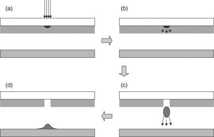
18.2 Schematic representation of the steps involved in the forward transfer of rheological systems during the LDW process. (a) The laser pulse is absorbed in the ink layer adjacent to the transparent glass plate. (b)The absorbed energy causes solvent vaporization to occur and (c) propel a droplet away from the film. (d)Finally, the droplet splashes down on the substrate.
In reality, the process represents an important difference from prior LIFT technology as functional materials are deposited without direct vaporization, which under ambient conditions degrades their physical or chemical properties such as electrical conductivity, dielectric properties or electrochemical activity. As shown schematically in Fig. 18.2, for absorbing materials, a small region of the ink interacts with a low fluence (< 100 mJ/cm2) laser pulse, causing a small amount of the ink to evaporate. As the resulting vapor expands, it generates shear forces that result in the ejection of a droplet from the film, which is unaffected by the incident laser. The droplet is then propelled in jet-like fashion towards the receiving substrate, where it is deposited with its original rheological properties intact. The claim that most if not all of the transferred fluid does not interact with the laser pulse has been substantiated by the results obtained with transfers of extremely laser-sensitive systems, such as buffer solutions containing biomaterials, proteins and living cells (Wu et al., 2001), or electrochemically sensitive materials discussed below (Arnold et al., 2004a).
The capability offered by the LDW technique to conformally transfer viscous fluids, pastes or inks has been used with great success for the fabrication of metal interconnects, vias and antenna structures (Piqué et al., 2003; 2005). In fact, the LDW process has been used to deposit metallic screen-printable inks over complex 3-D surfaces, i.e. conformal coatings, which has always been extremely difficult if not impossible using traditional lithographic processes. For example, LDW of thick-film polymer or ceramic pastes has been used to fabricate passive electronic components such as resistors (Modi et al., 2001) and interdigitated capacitors (Young et al., 2001). The use of LDW to fabricate simple electronic circuits comprising several passive components and their interconnects has been demonstrated, as in the case of a simple chemoselective gas sensor circuit (Piqué et al., 2002) and RF filter test structures (Zhang et al., 2003).
18.4 Laser-printed micro-power sources
Recent advances in integration and processing techniques have enabled microelectronic and microelectromechanical devices to shrink in size dramatically. While these devices have been used as components in larger sensor, actuator and control systems, the lack of commensurately sized power sources has limited their ability to function autonomously. One solution to this challenge is to integrate the micropower sources directly into or adjacent to the microdevice, thus forming a self-sufficient system. The resulting savings in volume and weight would allow the development of truly miniaturized autonomous systems, such as those needed for distributed wireless sensor networks. In these types of applications, the necessary-size scale is on the order of microns to millimeters. Such a vision might become a reality with the use of techniques such as laser printing, laser micromachining and laser processing.
For the purposes of this chapter, we will consider energy-related electrochemical systems, such as ultracapacitors, batteries, or electrochemical solar cells, to be composed of three main internal components: the negative electrode or anode, the positive electrode or cathode, and the electrolyte/separator. Each of these materials typically has a large degree of structural complexity and comprises a wide range of materials, such as nanocomposites, solid-state polymers, liquids and mesoporous mixtures of electrochemically active materials. Micro- and meso-scale power sources employ similar types of materials, but the unique challenge is to maintain their electrochemical activity and structural integrity in a confined space subject to the limitations, such as temperature and pressure, imposed by the microdevices, their substrates and their packaging.
To meet the power demands of a given microdevice, combinations of different types of power source are needed (Koeneman et al., 1997). For instance, an application may require constant low power, supplied by a lithium or alkaline microbattery, or an occasional short burst of energy, supplied by an ultracapacitor, combined with long intervals in ‘stand-by’ mode, during which recharging takes place by harvesting energy from the environment supplied by a solar cell. The laser-printing techniques described in this chapter are ideally suited to prototype, optimize and fabricate these electrochemical components. Advanced laser techniques can also embed the electrochemical components directly within a substrate, further reducing the packaged size of an entire microdevice, while allowing their geometry to be adapted to fit virtually any form factor.
In constructing electrochemical cells for energy storage and power generation, it is instructive to consider the desired operating geometries. The two main approaches include placing the anode and cathode adjacent to each other in the same plane (planar), or layering the anode and cathode on top of one another (stacked). There are particular advantages and disadvantages to each of these different geometries. In the case of stacked geometries, one can obtain higher area densities and lower resistances owing to the relatively thin separator layer, but this layer must be structurally stable to support the anode, cathode and associated current collectors. This feature rules out highly conductive gel and wet electrolytes. From a fabrication standpoint, planar geometries are easier to process since they can accommodate softer and rougher materials, but they have higher internal resistances due to the greater distance between the electrodes, and therefore tend to have lower performance at high currents. From a power density standpoint, stacked structures are more efficient but harder to fabricate using printing processes. With LDW, both planar and stacked structures have been demonstrated (Arnold et al., 2007). Using LDW, the printing speeds by which these structures can be deposited depends on the type of material being deposited and the desired feature resolution. For micro-power sources, the typical voxel size that can be printed by LDW with each laser pulse is about 100 micrometers square and about 5 micrometers thick. For a typical translation stage traveling at 1 m/s, a 10 kHz laser pulse rate would be sufficient to print 10 000 of such voxels in one second, covering an area of 1 cm2 each second with a layer 5 micrometers thick. So it is feasible to laser print the cathode, separator and anode layers required for a simple stacked 1 cm2 meso-scale battery in a few seconds.
18.4.1 Laser-printed ultracapacitors
Ultracapacitors based on a combination of sulfuric acid and hydrous ruthenium oxide have been successfully fabricated by laser-printing techniques (Arnold, 2004a). These electrochemical systems are conceptually the easiest to understand, as they form a planar structure that is symmetric, namely, the anode and cathode are made from the same materials. Furthermore, hydrous ruthenium oxide exhibits one of the largest specific capacitances of any material (Zheng et al., 1995), which will be exploited in these small-scale systems. Ultracapacitors, also known as supercapacitors or pseudocapacitors, are a class of electrochemical capacitor that exhibits large specific capacity (Conway, 1999). These systems display electronic properties similar to both batteries and capacitors. Like a capacitor, an ultracapacitor has the ability to discharge its energy very rapidly, leading to a high power density. However, like a battery, it has the ability to store a large amount of energy in the charge state of the active materials. In the most basic manner, we can think of an ultracapacitor as a battery with a high discharge rate. These devices are typically used for load leveling and applications where a short burst of power is needed.
The fundamental mechanisms for charge storage in these devices come from two possible sources. The first effect is similar to a typical capacitor in which the electrostatic double-layer at the interface between the electrode and electrolyte stores charge. A high surface area leads to large amounts of charge stored in the system. These effects are common in carbon-based ultracapacitor systems. The second effect stores charge through a Faradaic transfer at the surface of the electrode material. This is similar to the oxidation/reduction reactions that occur in a regular battery, but once again, the high surface area enables a large amount of charge storage and rapid charge transfer through this mechanism. These effects become relevant in metal oxide ultracapacitor systems. In either case, the discharge properties of the device resemble that of a capacitor. Namely, at constant current, the voltage across the device will decrease linearly with time.
Hydrous ruthenium oxide is an ideal electrode material for a micro-ultracapacitor due to its high specific capacitance (capacitance per unit mass). The rapid insertion and release of protons and electrons through the material enables a large pseudocapacitance effect, which, in combination with a high specific surface area, leads to the large amounts of charge stored in the material (Sarangapani et al., 1996; Trasatti and Kurzweil, 1994). This effect is enhanced by the presence of structural water in the lattice that provides nanostructured percolation pathways for proton conduction into the bulk of the material (Dmowski et al., 2002).
In the context of a small-scale ultracapacitor system, the main challenge is to produce electrodes that preserve the desirable electrochemical properties of the active material while maintaining the structure necessary for high surface area, subject to the process temperature/pressure limitations. These stringent requirements have made the growth of hydrous ruthenium oxide films incompatible with standard vacuum techniques such as physical or chemical vapor deposition for thin-film growth. Other thin-film techniques such as sol-gel techniques (Fang et al., 2001) or electrostatic spray deposition (Kim and Kim, 2001) are compatible with the material constraints, but require multiple processing steps, including additional lithography to produce the two-dimensional structures required for making microultracapacitors. Laser printing provides a solution to these challenges.
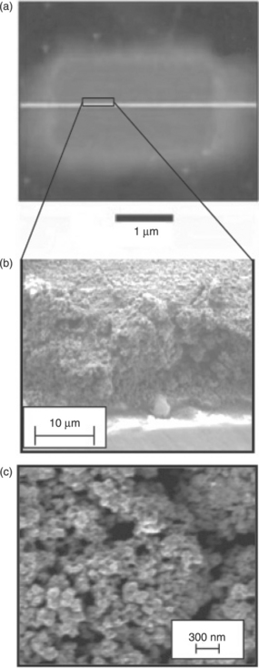
The laser printing of ultracapacitors starts with the preparation of an ink composed of an active material and a suitable transfer liquid. The ability to premix the electrode material with electrolyte gives LDW a distinct advantage over other direct-write methods such as ink-jet or MicroPen as it enables better control over impurities in the electrodes and has been shown to significantly improve the discharge behavior of these cells (Arnold et al., 2002). In general, any substrate and electrode geometry is possible, provided two electronically isolated current collectors are formed. The printed material is porous, exhibiting a random network of connected grains. This structure is ideally suited for the penetration of liquid or gel electrolyte, which enables a large surface area in contact with the electrolyte for charge transfer. This in turn leads to better utilization of the electrode material and improved transport throughout the electrode. LDW is unique in comparison to other deposition techniques in its ability to create these electrochemically desirable structures on the mesoscale. An encapsulating layer of Nafion® is placed on top of the structure and a droplet of sulfuric acid is added to assure a fully saturated membrane. Characterization of the laser-printed ultracapacitors has shown that these cells can be discharged at currents above 50 mA and can be connected in series and parallel combinations to yield the proper voltage values (Arnold et al., 2003). The overall size and mass of these systems is small at < 100 μg, while the power output is above 1 mW. Dual laser techniques, used to remove the electrolyte locally and then micromachine gaps to isolate the electrodes (Arnold et al., 2004c) have also been demonstrated. These dual laser techniques enable a level of process optimization toward the ultimate goal of high-throughput fabrication. Figure 18.3 shows a micrograph of such a planar ultracapacitor laser-printed on a glass substrate and SEM images illustrating the mesoporous structure of the laser-printed hydrous ruthenium oxide electrode.
18.4.2 Laser-printed microbatteries
With batteries, the stored chemical energy is converted to electrical energy through oxidation and reduction reactions at the electrodes. Electrons generated by oxidation of the anode material generate work in the electrical circuit before recombining to reduce the cathode material. The separator/electrolyte enables the flow of ions between the anode and cathode to complete the circuit. The large number of chemical possibilities are discussed and reviewed in readily available reference books (Linden and Reddy, 2001; Vincent and Scrosati, 1997).
In the case of small-scale microbatteries, the main challenge is to create mesoscale patterns of these active materials while maintaining the necessary physical and chemical properties of a functioning cell. There has been significant effort to develop small microbatteries for various primary and secondary chemistries. Examples include secondary solid-state lithium-ion cells in a stacked configuration (Arnold et al., 2004a; Bates et al., 1995, 2000) and primary alkaline microbatteries in a planar configuration where the anode and cathode are located adjacent to each other on the substrate (Arnold et al., 2004c; Humble et al., 2001; LaFollette et al., 2001).
18.4.3 Primary alkaline batteries made by laser printing
Alkaline batteries are one of the most ubiquitous battery chemistries in use today. Their low cost, relative environmental safety and high discharge rates make them readily available for consumer applications. In comparison to other alkaline chemistries, the zinc/silver oxide (Zn-Ag2O) system has found extensive use in applications that require maintaining a constant voltage throughout the battery discharge. Primary Zn-Ag2O alkaline microbatteries have been demonstrated using LDW techniques by laser-printing zinc and monovalent silver oxide (Ag2O) powders in both planar and stacked geometries on a variety of substrates (Arnold et al., 2004a, 2004b; Piqué et al., 2004b). The typical weight of all laser-printed material is 250 μg, while the thickness of the anode and cathode layers is about 10–20 μm. In order to activate the planar cells, a drop of 25 wt% KOH solution is placed on the electrodes. Figure 18.4 shows micrographs from sample alkaline microbatteries made by laser printing.
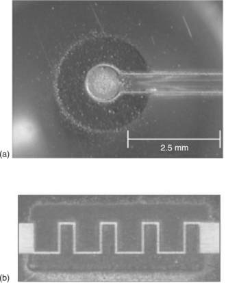
18.4 Optical micrographs of two laser-printed planar alkaline microbatteries′ configurations: (a) ring-shaped with a zinc center electrode and an outer silver oxide electrode; (b) interdigitated arrangement with silver oxide top and zinc bottom electrodes.
Electrochemical evaluation of the cell voltage and discharge behavior of the alkaline microbatteries demonstrated similar behavior to that of larger cells. The open-circuit potential for both planar and stacked microbatteries was 1.55 V, while their discharge at constant currents showed the characteristic flat response of the Zn-Ag2O alkaline system. High capacity cells are obtained in this manner. For instance, planar cells have been fabricated with capacities greater than 450 mAhr/cm2. An important challenge remains in how to package these cells for commercial use. Since a liquid consisting of a highly corrosive alkaline solution is used as the electrolyte of the Zn-Ag2O microbatteries, sealing these tiny structures is not easily achieved without compromising their size and wasting significant mass and footprint on the packaging. A better alternative would be to fabricate ‘dry’ microbatteries, where issues such as leakage and contamination of the electrolyte are not as critical, or employ embedding strategies as discussed later in the chapter. For example, ionic liquids can be used to create new types of solid state cells that mimic standard alkaline cells, without the need for highly acidic or basic electrolytes. At the US Naval Research Laboratory, ionic liquids are being studied both as the electrolyte/separator in primary solid state batteries, and as a reactive species in the cell’s electrochemical makeup (Sutto et al., 2011).
18.4.4 Secondary batteries made by laser printing
Lithium microbatteries offer significantly higher energy densities than other rechargeable battery systems owing to the small size of Li and its high reduction potential. Secondary lithium ion intercalation microbatteries have been fabricated by laser printing LiCoO2 powders for the cathode and graphite powders for the anode in stacked geometries.
Two types of separators have been used to make the lithium cells. In one case, porous polymer membranes were laser cut and placed between the cathode and anode layers (Wartena et al., 2004), while on the other an ionically conductive polymer nanocomposite membrane was laser-printed on top of the cathode layer (Sutto et al., 2006). The LiCoO2 cathodes and carbon anodes were deposited by LDW onto aluminum and copper foils, respectively. Characterization of the charge/discharge cycling performance (C/18 rate) of a packaged Li-ion microbattery demonstrated the expected behavior for the LiCoO2/Li system. Typical laser-printed microbatteries had a charge/discharge efficiency of ~ 98% and a capacity per unit area of 205 μAhr/cm2, which compares favorably to the value of 163 μAhr/cm2 achieved for sputter-deposited Li microbatteries reported by Bates and colleagues (Bates et al., 2000).
LDW techniques can also be used to print thick-film electrodes for microbatteries with a significantly higher discharge capacity, power and energy densities than those made by sputter-deposited thin-film techniques. This increased performance is attributed to the porous structure of the laser-printed electrodes, which allows improved ionic and electronic transport through the thick-film electrodes (~ 100 μm) without a significant increase in internal resistance (Kim et al., 2007). Figure 18.5 shows the cross-section of a Li-ion microbattery made by LDW as well as SEM images of the cathode and anode laser-printed electrodes. When compared to other types of microbatteries, such as thin-film microbatteries, the laser-printed thick-film microbatteries deliver significantly higher discharge capacities (~ 2586 μAh/cm2) at a current density of 100 μA/cm2 than those reported for sputter-deposited thin-film microbatteries (~ 160 μAh/cm2) (Kim et al., 2007).
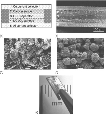
18.5 (a) Cross-sectional schematic diagram (not to scale) of a typical Li- on microbattery. (b) Cross-sectional SEM micrograph of a packaged thick-film Li-ion microbattery. (c) SEM image of a laser-printed LiCoO2 cathode. (d) SEM image of a laser-printed carbon anode. (e) Optical micrograph of a packaged Li microbattery made by LDW.
18.4.5 Laser-printed dye-sensitized photovoltaics
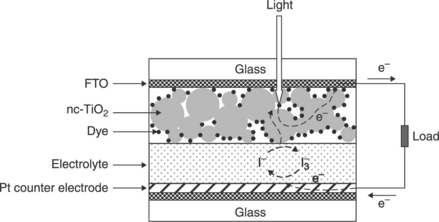
DSSC are a photosensitive electrochemical cell with a more complicated electrode configuration in comparison to the ultracapacitors and microbatteries previously discussed. The anode in this case comprises light-absorbing dye molecules attached to the surface of nanocrystalline-TiO2 (nc-TiO2) particles. The electrons generated by oxidation of the dye molecules are injected into the conduction band of the wide band-gap TiO2 and transported to the external circuit through a transparent conducting oxide layer. On the cathode side, a metal catalyst enables the direct reduction of the electrolyte itself (I−/I3−), which subsequently reduces the oxidized dye molecules to their initial state. The schematic structure of a DSSC is shown in Fig. 18.6.
Over the last decade, DSSCs based on nc-TiO2 films have been extensively studied as possible alternatives to silicon-based solar cells due to their high power conversion efficiencies (~ 10%) and expected low materials and manufacturing costs (Barbe et al., 1997; Nakada et al., 2002; Nazeeruddin et al., 1993; O’Regan and Grätzel, 1991). Mesoporous nc-TiO2 layers with high surface area are essential for achieving high efficiency in the DSSC system because a large amount of dye can be adsorbed on the surface of the nc-TiO2 particles resulting in an increased solar light absorption and an increased reacting interface per unit area.
The general structure of a LDW DSSC is similar to the stacked geometry described in the previous sections on microbatteries. However, in this case, we use traditional vapor deposition to create the transparent conducting oxide layers and Pt cathode. The inks used are made from water-based colloidal suspensions of nc-TiO2 powders mixed with organic additives. Mesoporous, nc-TiO2 films are deposited onto fluorine-doped tin oxide (FTO)-coated glass substrates by laser printing of these inks (Kim et al., 2004, 2005). The transferred films are dried in air and sintered in the oven at 450 °C for 30 minutes. Once the films are sintered, the electrode is soaked in the dye solution in order to coat the TiO2 surface. Finally, the completed cells are assembled and sealed using a Surlyn gasket to separate the anode and cathode layers and provide a reservoir for the I−/I3− electrolyte. As with the laser-printed microbatteries, the transferred materials maintain a homogeneously distributed network of particles with a high degree of porosity, consistent with a high surface area structure.
Laser-printed dye-sensitized solar cells (DSSCs) made with an optimum thickness of 15 μm exhibited a Jsc of 10.1 mA/cm2, Voc of 0.64 V, a fill factor (ff) of 0.65 and a light power conversion efficiency (η) of ~ 4.3 %. The conversion efficiency is comparable to those reported earlier for analogous cells fabricated with commercial TiO2 powders (P25) using traditional techniques such as screen printing or stenciling (Hinsch et al., 2001; Nakada et al., 2002; Okuya et al., 2002). Using laser-sintering techniques, it is possible to remove the 450 °C oven curing step from the overall process (Kim et al., 2005). The power conversion efficiency of the devices based on the laser-sintered nc-TiO2 electrodes is a factor of two greater than non-sintered films, but still less than what can be obtained from high-temperature processes. Nevertheless, use of such laser processing techniques allows the transfer of the TiO2 colloidal suspensions and in situ sinter of the mesoporous nc-TiO2 electrodes using the same UV laser, thus simplifying the processing steps required for fabricating DSSCs at low-temperatures and making them compatible with low-temperature substrates such as flexible polymers. Further optimization of the laser sintering conditions such as power intensity, laser beam spot size and translation speed leave ample room for refinement.
18.5 Laser-printed embedded micro-power sources
One of the important issues for microbatteries and other small-scale electrochemical systems is the development of an appropriate packaging scheme that protects the device from environmental degradation and preserves its small size. In order to address this issue, one can utilize more advanced surface restructuring and processing than is possible with laser printing techniques.
In many cases where microbatteries are required, one desires to place the cell directly on the substrate of the microdevice to be powered. In these cases, one can take advantage of the existing substrate as a packaging material by placing the battery within the substrate rather than on top of the substrate. For instance, in the case of fiberglass or polyimide circuit boards, one can laser-micromachine pockets of desired dimensions and deposit each of the electrode layers inside, as shown in Fig. 18.7. The problem is then reduced to sealing the top of the battery with a metallic current collector to produce a fully embedded solution. With further refinements, one can create a separator layer from the substrate itself by laser micromachining both top and bottom to leave a thin layer of polymer or fiberglass before refilling it from both sides. In the case of solid-state Li-ion microbatteries, it is also possible to LDW all the layers inside a well within the substrate, as shown in Fig. 18.7(b). The ability to completely transfer and assemble electrochemically and thermally stable micropower sources into bulk materials can be extended to more advanced applications in which the power source is directly incorporated and sealed within the substrates used by the microdevice (Arnold et al., 2004d).

18.7 (a) Schematic showing an embedded Li-ion microbattery in cross-section view. (b) Optical micrograph of a laser-printed solid-state Li-ion microbattery embedded in a polyimide substrate.
Progress towards printing fully embedded micropower sources requires the implementation of alternative material systems for the electrodes and separator layers. For example, Li-ion batteries use a liquid electrolyte, which causes drawbacks in areas of packaging, cost, safety and size when trying to develop a micro-battery. In order to overcome these limitations, it is important to replace the liquid electrolyte with a solid-state polymer electrolyte. This would allow for easier packaging with less material. Also, these polymer electrolytes can be made much thinner than the currently used permeable membranes. Using a solid-state polymer as an electrolyte also eliminates safety concerns, since the volatility of the liquid electrolyte is no longer an issue. Ionically conductive solid-state electrolyte membranes have been incorporated into fully functional prototype embedded Li-ion microbatteries by LDW techniques (Ollinger et al., 2006).
18.6 Challenges and opportunities
The use of laser printing, laser micromachining and laser sintering techniques for the transfer, removal and processing of electronic and power-generating materials has been reviewed in the previous sections. Numerous examples of the types of components fabricated using these techniques are described, and it is clear that these processes, referred to as LDW, are well suited to transferring or printing inks or fluids containing suspensions or mixtures of the required power-generating materials. The cured inks form conformal patterns that are continuous and well-adhered to the substrate and are used to generate patterns of mesoporous structures with extremely high effective surface areas required in the fabrication of micropower devices such as ultracapacitors, microbatteries and DSSCs. Each of these is an indispensable element in the fabrication of autonomous, self-powered microelectronic systems such as wireless sensor networks. However, in order to reach the full potential of the LDW processes, it is desired that these elements be integrated into fully functional circuits.
Work toward this goal is progressing rapidly. Laser forward transfer and LDW techniques are poised to play an important role in the development of the next generation of electronic systems as work toward the goal of complete device integration steadily progresses. For example, future microelectronic designs will require integration of many different and increasingly smaller components. To achieve this, it is necessary to accurately place small-scale energy storage systems and individual electrical components such as semiconductor bare die and submillimeter discrete passive components on surfaces that may not be compatible with traditional ‘pick-and-place’ equipment. The placement of each of these components onto virtually any type of surface is enabled by the use of laser transfer methods.
An alternative approach to device integration and miniaturization can be accomplished by incorporating electronic components, energy storage, and their interconnects within the volume of a substrate. Rather than limiting their placement to its surface, it will be possible to integrate electronic circuits within any type of form factor. The development of such ‘embedded’ electronics is being explored using LDW techniques. Embedded surface-mount devices (SMDs), semiconductor bare die integrated circuits (ICs), interconnects and power source elements, offer the ability to achieve levels of miniaturization beyond the capabilities of current manufacturing techniques. Given an arbitrary circuit design, significant reductions in volume and overall weight can be achieved by using embedded components. Furthermore, embedded circuits exhibit higher device density and improved electrical performance, resulting in enhanced functionality within a given form factor. In the past few years, various demonstrations of the use of LDW techniques for the fabrication of embedded electronic circuits have been published (Piqué et al., 2004a, 2005; Wang et al., 2010).
18.7 Conclusion and future trends
Laser printing processes and other LDW techniques are enabling technologies for the fabrication of various types of micro- and mesoscale power-generating devices such as ultracapacitors, DSSCs and microbatteries, both primary and rechargeable, as the prior sections have shown. Notably, the laser printing process is not chemistry-specific, allowing different types of materials to be deposited using the same tool by simply changing the source ribbon. More advanced techniques, such as deposition of a liquid phase polymer nanocomposite that dries into a solid, ionically conductive micron-thick solid separator, or the removal of material from a surface via laser micromachining for embedded structures, make possible other types of microelectrochemical cells that can be incorporated into a wide variety of microdevices.
LDW techniques encompass many laser-based processes, which allow the subtraction (i.e. laser micromachining), addition (i.e. laser transfer) and modification (i.e. laser annealing) of many types of materials. As this chapter has shown, LDW can be used for the generation of mesoscale patterns of electronic and power-generating materials directly on a substrate without requiring lithographic processing. These patterns can be assembled to form simple structures such as metal lines for establishing the connections between devices in functional circuits, or more complex ones such as the multilayers required for a stacked Li-ion microbattery. The energy storage devices fabricated through these techniques exhibit outstanding performance characteristics. In each case, the ability to transfer complex suspensions from a ribbon to an acceptor substrate under ambient conditions and without changing their physical or chemical properties is one of the unique attributes of the LDW process. Another key attribute of LDW processes is that they can be used for rapid prototyping applications, allowing the design, fabrication and testing of a given structure to be carried out quickly.
The recent application of LDW techniques for the transfer of preformed devices such as semiconductor bare dies, and for embedding microbatteries and simple electronic circuits, opens the door for the development of a unique laser-based microelectronics fabrication tool. Such a tool would be capable of fabricating and embedding electronic circuits with the required power storage and power-harvesting components within the same substrate. The resulting fully integrated systems could easily be reconfigured to fit within a desired form factor, thus allowing the placement of electronic systems in places that seem inconceivable today. Such a system, although not yet available, would play a very important role in the development of next generation sensor networks and autonomous systems. Given LDW’s ability to print not only the power sources but also the associated electronics, the rapid manufacture of fully functional application specific sensor nodes would be as easy as it is today to print a 3D model.
18.8 Acknowledgements
The author would like to thank all the members of the LDW group at the Naval Research Laboratory. Special thanks to Heungsoo Kim, Craig Arnold, Mike Ollinger, Ray Auyeung and Tom Sutto. This work was sponsored by the US Office of Naval Research.
18.9 References
Adrian, F.J., Bohandy, J., Kim, B.F., Jette, A.N., Thompson, P. A study of the mechanism of metal deposition by the laser-induced forward transfer process. Journal of Vacuum Science and Technology. 1987; B5:1490–1494.
Arnold, C.B., Wartena, R.C., Pratap, B., Swider-Lyons, K.E., Piqué, A., Laser direct writing of hydrous ruthenium dioxide micro-pseudocapacitors Vol. 689Chrisey D.B., Danforth S.C., eds. Electroactive polymers and rapid prototyping. Materials Research Society: Pittsburgh, PA, 2002:275–280.
Arnold, C.B., Wartena, R.C., Swider-Lyons, K.E., Piqué, A. Direct-write planar micro-ultracapacitors by laser engineering. Journal of Electrochemical Society. 2003; 150:A571–A575.
Arnold, C.B., Kim, H., Sutto, T.E., Piqué, A. Direct write laser processing for miniature electrochemical systems. Laser Focus World. 2004; 40:9–12.
Arnold, C.B., Kim, H., Piqué, A. Laser transferred primary alkaline microbatteries. Applied Physics A. 2004; 79:417–420.
Arnold, C.B., Piqué, A. Self-filling wet electrochemical cells by laser processing, 2004. [US patent application 20040256359].
Arnold, C.B., Piqué, A., Auyeung, R.C.Y., Nurnberger, M. Laser-based technique for producing and embedding electrochemical cells and electronic components directly into circuit board materials, 2004. [US patent application 2005000613].
Arnold, C.B., Serra, P., Piqué, A. Laser direct-write techniques for printing of complex materials. MRS Bulletin. 2007; 32:23–31.
Auyeung, R.C.Y., Wu, H.D., Modi, R., Piqué, A., Fitz-Gerald, J.M., et al. Matrix-assisted laser transfer of electronic materials for direct-write applications. Proceedings of SPIE. 2000; 4088:393–396.
Bähnisch, R., Gross, W., Menschig, A. Single-shot, high repetition rate metallic pattern transfer. Microelectronic Engineering. 2000; 50:541–546.
Barbe, C.J., Arendse, F., Comte, P., Jirousek, M., Lenzmann, F., et al. Nanocrystalline titanium oxide electrodes for photovoltaic applications. Journal of American Ceramic Society. 1997; 80:3157–3171.
Bates, J.D., Dudney, N.J., Lubben, D.C., Gruzalski, G.R., Kwak, B.S., et al. Thin-film rechargeable lithium batteries. Journal of Power Sources. 1995; 54:58–62.
Bates, J.B., Dudney, N.J., Neudecker, B., Ueda, A., Evans, C.D. Thin-film lithium and lithium–ion batteries. Solid State Ionics. 2000; 135:33–45.
Bohandy, J., Kim, B.F., Adrian, F.J. Metal deposition from a supported metal film using an excimer laser. Journal of Applied Physics. 1986; 60:1538–1539.
Bohandy, J., Kim, B.F., Adrian, F.J., Jette, A.N. Metal deposition at 532 nm using a laser transfer technique. Journal of Applied Physics. 1988; 63:1158–1162.
Conway, B.E. Electrochemical supercapacitors, scientific fundamentals and technological applications. New York: Kluwer Academic; 1999.
Dmowski, W., Egami, T., Swider-Lyons, K.E., Love, C.T., Rolison, D.R. Local atomic structure and conduction mechanism of nanocrystalline hydrous RuO2 from x-ray scattering. Journal of Physical Chemistry B. 2002; 106:12 677–12 683.
Esrom, H., Zhang, J.-Y., Kogelschatz, U., Pedraza, A.J. New approach of a laser-induced forward transfer for deposition of patterned thin metal films. Applied Surface Science. 1995; 86:202–207.
Fang, Q.L., Evans, D.A., Roberson, S.L., Zheng, J.P. Ruthenium oxide film electrodes prepared at low temperatures for electrochemical capacitors. Journal of Electrochemical Society. 2001; 148:A833–A837.
Fernández-Pradas, J.M., Colina, M., Serra, P., Dominguez, J., Morenza, J.L. Laser-induced forward transfer of biomolecules. Thin Solid Films. 2004; 453–454:27–30.
Fogarassy, E., Fuchs, C., Kerherve, F., Hauchecorne, G., Perriere, J. Laser-induced forward transfer of high-TcYBaCuO and BiSrCaCuO superconducting thin films. Journal of Applied Physics. 1989; 66:457–459.
Greer, J.A., Parker, T.E. Laser-induced forward transfer of metal oxides to trim the frequency of surface acoustic wave resonator devices. Proceedings of SPIE. 1988; 998:113–125.
Herman, I.P. Laser-assisted deposition of thin films from gas-phase and surface-adsorbed molecules. Chemical Reviews. 1989; 89:1323–1357.
Hinsch, A., Kroon, J.M., Kern, R., Uhlendorf, I., Holzbock, J., et al. Long-term stability of dye-sensitized solar cells. Journal of Progress in Photovoltaics: Research and Applications. 2001; 9:425–438.
Humble, P.H., Harb, J.N., LaFollettte, R. Microscopic nickel–zinc batteries for use in autonomous microsystems. Journal of Electrochemical Society. 2001; 18:A1357–A1361.
Kántor, Z., Tóth, Z., Szorenyi, T., Tóth, A.L. Deposition of micrometer-sized tungsten patterns by laser transfer technique. Applied Physics Letters. 1994; 64:3506–3508.
Karaiskou, A., Zergioti, I., Fotakis, C., Kapsetaki, M., Kafetzopoulos, D. Microfabrication of biomaterials by the sub-ps laser-induced forward transfer process. Applied Surface Science. 2003; 208–209:245–249.
Kim, H., Kushto, G.P., Arnold, C.B., Kafafi, Z.H., Piqué, A. Laser processing of nanocrystalline TiO2 films for dye-sensitized solar cells. Applied Physical Letters. 2004; 85:464–466.
Kim, H., Auyeung, R.C.Y., Ollinger, M., Kushto, G.P., Kafafi, Z.H., Piqué, A. Laser-sintered mesoporous TiO2 electrodes for dye-sensitized solar cells. Applied Physics A. 2005; 83(1):73–76.
Kim, H., Auyeung, R.C.Y., Piqué, A. Laser-printed electrodes for solid-state rechargeable Li-ion microbatteries. Journal of Power Sources. 2007; 165:413–419.
Kim, I.H., Kim, K.B. Ruthenium oxide thin film electrodes for supercapacitors. Electrochem. Solid-State Letters. 2001; 5:A62–A64.
Koeneman, P.B., Busch-Vishniac, I.J., Wood, K.L. Feasibility of micro power supplies for MEMS. Journal of Microelectromechical Systems. 1997; 6:355–362.
LaFollettte, R., Harb, J.N., Humble, P., Sixteenth Annual Battery Conference: Applications and Advances. R.S.L. Das, H. Frank. IEEE, Piscatawy, NJ, 2001.:349–354.
Linden, D., Reddy, T.B., Handbook of batteries, 3rd edn. McGraw-Hill, New York, 2001.
Modi, R., Wu, H.D., Auyeung, R.C.Y., Gilmore, C.M., Chrisey, D.B. Direct writing of polymer thick-film resistors using a novel laser transfer technique. Journal of Material Research. 2001; 16:3214–3222.
Nakada, S., Matsuda, M., Kambe, S., Saito, Y., Kitamura, T., et al. Dependence of TiO2 nanoparticle preparation methods and annealing temperature on the efficiency of dye-sensitized solar cells. Journal of Physical Chemistry B. 2002; 106:10 004–10 010.
Nazeeruddin, M.K., Kay, A., Rodicio, I., Humphry-Baker, R., Muller, E., et al. Conversion of light to electricity by cis-X2Bis(2,2′-bipyridyl-4,4′-dicarboxylate) ruthenium(II) charge-transfer sensitizers (X = Cl−, Br−, I−, CN− and SCN−) on nanocrystalline TiO2 electrodes. Journal of American Chemical Society. 1993; 115:6382–6390.
Okuya, M., Nakade, K., Kaneko, S. Porous TiO2 thin films synthesized by a spray pyrolysis deposition (SPD) technique and their application to dye-sensitized solar cells. Solar Energy Materials and Solar Cells. 2002; 70:425–435.
Ollinger, M., Kim, H., Sutto, T., Piqué, A. Laser printing of nanocomposite solid-state membranes for Li micro-batteries. Applied Surface Science. 2006; 252:8812–8816.
O’Regan, B., Grätzel, M. A low-cost, high-efficiency solar cell based on dye-sensitized colloidal TiO2 films. Nature. 1991; 353:737–740.
Osgood, R.M., Deutsch, T.F. Laser-induced chemistry for microelectronics. Science. 1985; 227:709–714.
Papakonstantinou, P., Vainos, N.A., Fotakis, C. Microfabrication by UV femtosecond laser ablation of Pt, Cr and indium oxide thin films. Applied Surface Science. 1999; 151:159–170.
Pimenov, S.M., Shafeev, G.A., Smolin, A.A., Konov, V.I., Vodolaga, B.K. Laser-induced forward transfer of ultra-fine diamond particles for selective deposition of diamond films. Applied Surface Science. 1995; 86:208–212.
Piqué, A., Chrisey, D.B., Auyeung, R.C.Y., Lakeou, S., Chung, R., et al. Laser direct writing of circuit elements and sensors. Proceedings of SPIE. 1999; 3618:330–339.
Piqué, A., Chrisey, D.B., Auyeung, R.C.Y., Fitz-Gerald, J., Wu, H.D., et al. A novel laser transfer process for direct writing of electronic and sensor materials. Applied Physics A. 1999; A69:279–284.
Piqué, A., Chrisey, A.D.B., Fitz-Gerald, J.M., McGill, R.A., Auyeung, R.C.Y., et al. Direct writing of electronic and sensor materials using a laser transfer technique. Journal of Material Research. 2000; 15:1872–1875.
Piqué, A., Fitz-Gerald, J., Chrisey, D.B., Auyeung, R.C.Y., Wu, H.D., et al. Direct writing of electronic materials using a new laser assisted transfer/annealing technique. Proceedings of SPIE. 2000; 3922:105–112.
Piqué, A., Weir, D.W., Wu, P.K., Pratap, B., Arnold, C.B., et al. Direct-write of sensor devices by a laser forward transfer technique. Proceedings of SPIE. 2002; 4637:361–368.
Piqué, A., Arnold, C.B., Pratap, B., Auyeung, R.C.Y., Kim, H., et al. Laser direct-write of metal patterns for interconnects and antennas. Proceedings of SPIE. 2003; 4977:602–608.
Piqué, A., Mathews, S.A., Auyeung, R.C., Ollinger, M., Kim, H., et al. Application of laser direct-write techniques for embedding electronic and micropower components. Proceedings of SPIE. 2004; 5662:564–569.
Piqué, A., Arnold, C.B., Kim, H., Ollinger, M., Sutto, T.E. Rapid prototyping of micro-power sources by laser direct-write. Applied Physics A. 2004; 79:783–786.
Piqué, A., Pratap, B., Mathews, S.A., Karns, B.J., Auyeung, R.C., et al. Laser direct-write of embedded electronic components and circuits. Proceedings of SPIE. 2005; 5713:223–230.
Sarangapani, S., Tilak, B., Chen, C. Materials for electrochemical capacitors. Journal of Electrochemical Society. 1996; 143:3791–3799.
Schultze, V., Wagner, M. Laser-induced forward transfer of aluminum. Applied Surface Science. 1991; 52:303–309.
Serra, P., Colina, M., Fernández-Pradas, J.M., Sevilla, L., Morenza, J.L. Preparation of functional DNA microarrays through laser-induced forward transfer. Applied Physics Letters. 2004; 85:1639–1641.
Sutto, T.E., Ollinger, M., Kim, H., Arnold, C.B., Piqué, A. Laser transferable polymer-ionic liquid separator/electrolytes for solid-state rechargeable lithium ion microbatteries. Electrochemical Solid-State Letters. 2006; 9:A69–A71.
Sutto, T.E., Duncan, T.T., Wong, T.C., McGrady, K. Ionic liquid batteries: chemistry to replace alkaline/acid energy storage devices. Electrochem Acta. 2011; 56:3375–3379.
Tolbert, W.A., Lee, I.-Y.S., Doxtader, M.M., Ellis, E.W., Dlott, D.D. High-speed color imaging by laser ablation transfer with a dynamic release layer: fundamental mechanisms. Journal of Imaging Science Technology. 1993; 37:411–421.
Tolbert, W.A., I-Yin Sandy Lee, Wen, Xiaoning, Dlott, D.D., Doxtader, M.M., et al. Laser ablation transfer imaging using picosecond optical pulses: ultra-high speed, lower threshold and high resolution. Journal of Imaging Science Technology. 1993; 37:485–489.
Tóth, Z., Szorenyi, T., Tóth, A.L. Ar+ laser-induced forward transfer (LIFT): a novel method for micrometer-size surface patterning. Applied Surface Science. 1993; 69:317–320.
Trasatti, S., Kurzweil, P. Electrochemical supercapacitors as versatile energy stores. Platinum Metals Review. 1994; 38:46–56.
Vincent, C.A., Scrosati, B., Modern batteries, 2nd edn. Arnold, London, 1997.
Wang, J., Auyeung, R.C.Y., Kim, H., Charipar, N.A., Piqué, A. Three-dimensional printing of interconnects by laser direct-write of silver nanopastes. Advanced Materials. 2010; 22:4462–4466.
Wartena, R.C., Curtright, A.E., Arnold, C.B., Piqué, A., Swider-Lyons, K.E. Li-ion microbatteries generated by laser direct write. Journal of Power Sources. 2004; 126:193–202.
Wu, P.K., Ringeisen, B.R., Callahan, J., Brooks, M., Bubb, D.M., et al. The deposition, structure, pattern deposition and activity of biomaterial thin-films by matrix-assisted pulsed-laser evaporation (MAPLE) and MAPLE direct write. Thin Solid Films. 2001; 389–399:607–614.
Young, D., Wu, H.D., Auyeung, R.C.Y., Modi, R., Fitz-Gerald, J., et al. Dielectric properties of oxide structures by a laser-based direct-writing method. Journal of Materials Research. 2001; 16:1720–1725.
Zergioti, I., Mailis, S., Vainos, N.A., Papakonstantinou, P., Kalpouzos, C., et al. Microdeposition of metal and oxide structures using ultrashort laser pulses. Applied Physics A. 1998; 66:579–582.
Zergioti, I., Malilis, S., Vainos, N.A., Fotakis, C., Chen, S., et al. Microdeposition of metals by femtosecond excimer laser. Applied Surface Science. 1998; 127–129:601–605.
Zergioti, I., Karaiskou, A., Papazoglou, D. G., Fotakis, C., Kapsetaki, M. et al. Femtosecond laser microprinting of biomaterials, Applied Physics Letters, 86: 163902-1–163902-3.
Zhang, C., Liu, D., Mathews, S.A., Graves, J., Schaefer, T.M., et al. Laser direct-write and its application in low temperature co-fired ceramic (LTCC) technology. Microelectronic Engineering. 2003; 70:41–49.
Zheng, J.P., Cygan, P.J., Jow, T.R. Hydrous ruthenium oxide as an electrode material for electrochemical capacitors. Journal of Electrochemical Society. 1995; 142:2699–2703.