
Printed semiconducting gas sensors
Dedication: In memory of Professor Giuliano Martinelli – a wonderful person and an eminent scientist.
Abstract
Most common metal-oxide semiconductors featuring chemo-resistive effect, such as SnO2, TiO2, WO3 and ZnO, have been examined as functional materials for gas sensors via thick-film technology. Analysis of the mainly accepted electrical transport models through polycrystalline semiconductors has been carried out and compared to experimental evidence. A theoretical conduction model able to determine the characteristic length below which a material can be properly considered as nanostructured has been considered under thermionic and field-assisted electron emissions. The main methods of material synthesis have been extensively described with special attention to wet chemical routes for powder preparation. The typical parameters for screen-printable pastes obtained from the powders have been considered for deposition of the sensing layers. Electrical, structural and morphological characterizations have been explored in order to highlight the main features of the materials as pure compounds or in a mixture with other oxides. Finally, some concrete implementations carried out at our laboratory have been shown for the possible usage in environmental or industrial frameworks.
11.1 Introduction
Semiconductor gas sensors using metal oxides are a popular choice for detecting a wide range of gases. There is a variety of structures, materials and working principles used for semiconductor gas sensors. This chapter will review the most important types of semiconductor gas sensor and it will look at the printing technology for fabricating these sensors. In solid-state metal oxides, the difference in electro-negativity of a metal atom from oxygen changes the polarity of the electron distribution of bond orbitals, thus modulating the physical properties of the solid, including conductivity. In fact, metal oxides are an immensely wide class of materials whose electrical properties span over the full range of conductivity, from insulators to superconductors with semiconductors and metals in between. The high electro-negativity of oxygen renders this atom as negatively polarized, although there is a class of oxides where the metal-to-oxygen bond is weak enough to allow a reversible chemical redox reaction at the surface with a gaseous species. This condition is met for the metals with amphoteric behaviour, i.e. for which the difference in electro-negativity with oxygen is moderately low.
From the solid-state standpoint, this last occurrence forms a series of energy levels within the energy band-gap at the surface, which are filled up by electrons up to the Fermi level, depleting the volume of the solid neighbouring the surface of electrons. This process builds up a Schottky junction at the surface, which determines charge transport within the semiconductors (see section 11.2). Unlike Λ-probes, for which their elevated working temperature (about 1000 °C) forces diffusion of oxygen deep into the bulk of the material, within 200–600 °C, the interaction of gases with the sensing material occurs mainly at the surface. Thus, polycrystalline materials are recommended to magnify the extension of the surface exposed for reaction. It means that electrical conduction is governed by grain-to-grain percolation, which is in turn established by the height of the inter-grain barrier. Redox reaction of the anions and more rarely of the cations in the metal oxide with a gas causes charge exchange with the solid, leading to lowering or increasing of the energy barrier. In summary, current conduction in a metal oxide is established by the concentration of a gas in the surrounding atmosphere and this is normally referred to as a chemo-resistive effect, i.e. the transduction mechanism of solid-state semiconducting gas sensors (Madou and Morrison, 1989).
The first evidence of the dependence of electrical conductance on the concentration of gases in the environment dates back more than 50 years to a seminal work by Brattain and Bardeen (1953). However, the first generation of commercial devices was introduced in the 1960s by Taguchi, who established Figaro Engineering, Inc. The company’s target was the commercialization of small sensing units in the monitoring of explosive gases for Japanese urban agglomerates, which were characterized by wooden houses and widespread gas furnaces. The base material for the devices was SnO2 deposited via thick-film technology. Regarding the far-sightedness of this choice, we simply claim that Figaro Inc. is nowadays the largest manufacturer of gas sensors, SnO2 is commonly acknowledged as the ‘king material’ for gas-sensing and thick-film deposition is still the most widely used technique for the commercial production of sensors.
Since the pioneering scientific and commercial experiences, a big effort has been made to develop higher-performance sensing units over the years, fostered by the need for modern societies to monitor gaseous pollutants, malodours, volatile flammable substances, dangerous leaks and more. In this regard, chemo-resistive sensors grabbed the attention of researchers and investors in preference to other techniques because these sensors can be fabricated cheaply, are very compact and consume little power. In spite of these positive features, there are still drawbacks as highlighted in the following. In some senses, the so-called ‘3S-rule’, i.e. sensitivity, selectivity, stability, is a mandatory direction toward which research must be addressed.
Regarding sensitivity, a large contribution was made by the significant development that nanotechnology underwent in the 1990s, and it significantly impacted the field of gas sensing. The possibility of scaling down the grain size in the film proportionally enlarged the specific surface involved in gas sensing. In a seminal work, Yamazoe (1991) experimentally showed that a huge improvement in gas response was correlated to a decrease in grain size. Since then, nanophased semiconducting metal oxides have been pre-eminent candidates for gas sensing using the chemo-resistive effect. The level of sensitivity that is currently reached is quite satisfactory and makes any search for still higher sensitivity unnecessary at the present time.
The question of selectivity has not undergone the same boost as that of sensitivity. Chemical reaction at the surface of a given material normally proceeds for a variety of gaseous molecules, i.e. the sensor suffers a lack of selectivity. Indeed, operating with a gas admixture composed of different molecules that a semiconductor may interact with is certainly not unusual; ultimately, sensing in a humid environment is quite normal for working in on-field conditions, and water is unfortunately not an inert molecule for reaction. A first remedy is the use of catalysts in the form of nanoclusters (typically noble metals) spread over the surface of each grain. Except for some specific cases, heterogeneous catalysis ensures only partial solution of the problem, because the molecular species of interest very often lead to similar reactions. In the 1990s and early 2000s, a big effort was dedicated to the study of new materials (such as TiO2, In2O3, WO3, Fe2O3, ZnO, LaFeO3 and others) to investigate their sensing properties. In order to widen the choice of available materials, responding in a diverse way to a given analyte, strong doping, ternary oxides with two metals, in the form of either a mechanical mixture or a solid solution, were intensively investigated. The hope was that an array of films with partly overlapping sensing characteristics would aid the determination of single-species concentrations. Unfortunately the problem is not trivial because sensors respond non-linearly vs. a gas concentration, sometimes with strong cross-sensitivity between chemical species. Software architectures proved helpful in the problem of response deconvolution, in particular the approach relying on neural networks, and more generally in all the techniques of artificial olfactive systems that were adapted to gas sensing. To date, great progress has been made and, under some conditions, the problem of partial selectivity can be coped with, although in most general cases, it is still a problem for chemo-resistive gas sensing.
The last ‘S’ has been probably the toughest problem to solve. As previously mentioned, the rise in sensitivity called forward the use of nanophased materials, which are often in a metastable condition because of the large amount of energy deposited at the surface. This circumstance, combined with the need for keeping a sensor at operational temperature for reversible reaction with gases, often leads to grain coalescence, shrinkage of the specific surface, phase transition, phase segregations and other effects that spoil the response within a time shorter than the duration for which the sensor is designed. Several remedies have been proposed that lead to performance improvement, such as the dispersion of coalescence inhibitors and phase stabilizers for the nanograins, operation at room temperature via assistance from luminous excitation (to play the role that temperature normally does) and development of novel topologies in the nanomaterials. Regarding the latter, special attention must be paid to the advent of stable single-crystal quasi-one-dimensional semiconductors, normally referred to in the literature as quasi nanotubes, nanorods and nanoribbons, which are promising approaches whose real potential is still to be established (Comini et al., 2002).
The techniques for film preparation can be grouped into two categories depending either on the method used for material preparation, i.e. whether physical or chemical, or on the fashion used for film deposition, that is, thick-film or thin-film technology.
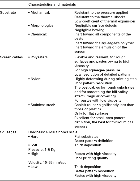
Thick-film deposition normally relies on screen-printing, which is one of the oldest forms of graphic art reproduction known to mankind. A typical thick-film screen consists of a finely woven mesh of stainless steel, polyester or nylon, mounted under tension on a metal loom. The finished screen has apertures for patterning and is held at suitable distance from the substrate. The thick-film paste is transferred onto the top surface of the stencil and a squeegee traverses the screen under pressure. This brings the screen closer to the substrate and forces the paste to flow through the apertures. Normally the pastes contain organic solvents that are needed to achieve the correct viscosity for screen-printing and after deposition they must be evaporated by drying at about 150–200 °C. After drying, adhesion of the film to the substrate is enhanced. Then further annealing is needed, called firing, during which the glass melts, the powders sinter and the film becomes a solid composite material. The function of glass is for binding the film to the substrate and to keep the particles together. Firing is performed in a furnace at a temperature ranging typically between 500 and 900 °C through proper ramping of the temperature, after which the film becomes firmly attached to the substrate. In the case of films for gas sensing, the firing serves also to stabilize the sensing material and to determine grain size and other film properties.
As far as our experience is concerned, one of the main advantages of screen-printing technology for the production of sensing layers is the inherent decoupling between material preparation and film deposition. Here such steps can be optimized separately. This is not the case for some techniques relying on thin-film preparation, for which preparation and deposition are accomplished all at once (e.g. Sberveglieri et al., 1990; Ferroni et al., 2003). For screen-printing deposition, nanometric powder preparation is made mainly via chemical wet methods, e.g. sol-gel synthesis, where catalysts, grain coalescence inhibitors can be added up to the precursors. As an alternative to sol-gel, laser-assisted (Musci et al., 1992) or flame-spray pyrolysis can also be used (Mädler et al., 2002). Then, proper thermal treatment (drying and firing) to stabilize the nanophase to the desired level can be pursued. Eventually, film deposition occurs with the right rheological parameters at the proper temperature. Optimizing this second step results in optimal film porosity and highly reproducible morphological and electrical properties. Porosity is a key parameter to be controlled: on the one hand, a highly densified aggregation of nanograins would ensure easy current percolation within the film with no critical bottle-neck pathways; on the other hand, too compact a film would result in scarce penetration of the gas-analyte and thereby in incomplete sensing by the volume of the film far from the surface.
The capability of thick-films to sense gases for a variety of applications has been proven over the years. Table 11.1 summarizes some of these gases though it is far from comprehensive and constitutes just an overview of the capability of the method. The table also contains a number of sensing materials used for the purpose.
Table 11.1
Examples of films achieved through thick-film technology
| Gas or vapour | Material | Reference |
| CO | SnO2 | Williams et al., 1994 |
| CO, NO2, CH4 | SnO2 | Guidi et al., 2002 |
| CO2 | BaTiO3 | Hauesler and Meyer, 1996 |
| Ethanol | Fe2O3 | Tan et al., 2004 |
| H2 | SnO2 | Ansari et al., 1996 |
| H2S, CH3SH, (CH3)2S | LaFeO3 | Chu and Siciliano, 2003 |
| HC and VOC | SnO2 | Pijolat et al., 2003 |
| Humidity | MnWO4 | Qu and Meyer, 1997 |
| NH3 | ZnO | Rao G. S. T. and Rao D. T., 1999 |
| NO2 | SnO2 | Sahm et al., 2004 |
| NO2 | Cr:TiO2 | Ruiz et al., 2003 |
| NO2 | WO3 | Choi et al., 2003 |
| NO2 | WO3 | Chung et al., 1999 |
| Oxygen | ZrO2 | Izu et al., 2004 |
| Reducing gases | Ga2O3 | Frank et al., 1996 |
| VOC, benzene, toluene, xylene | In:ZnO | Zhu et al., 2003 |
Thick-film technology is sometimes regarded as a ‘conservative approach’ to gas sensing via the chemo-resistive effect. Most modern proposals encompass sensing using novel schemes often based on methods borrowed from the technology of fully integrated circuits (e.g. suspended-gate field effect transistors). Screen-printing involves a hybrid technology and this is unlikely to be fully compatible with most futuristic schemes. However, sometimes this is not necessarily a limitation because problems can often be circumvented, as shown by the following example. A potential difficulty that could have risen with screen-printing technology was the implementation of film onto miniaturized micro-hotplates fabricated by silicon micro-fabrication. In some cases, low consumption is a desirable feature, e.g. for portable devices. The need to keep the sensing units at working temperature leads to thermal dissipation, mainly by thermal conductivity through the substrate. The use of thin micrometric insulating SiO2 membranes onto which a sensing film is deposited ensures operation at a nominal temperature with a power more than one order of magnitude lower than for the canonical case with a bulky substrate. The question of whether or not such a thin membrane was capable of tolerating the deposition of a screen-printed film that was ten times thicker was solved using a specifically designed chamfered stencil (Vincenzi et al., 2000).
In summary, we do believe that gas sensing through thick-film technology is, to date, one of the best ways to prepare sensing films for gas detection, its major features being good sensitivity and long-term stability, as witnessed by the use of such technology for producing the overwhelming majority of commercially available gas sensors.
11.2 Principles of operation and modeling
A classical view of the Schottky barrier formation at the surface through drift diffusion theory will be provided, which will be followed by the semi-classical approach to thermionic and field emission in nanostructures. This model for charge-carrier percolation holds for polycrystalline materials, no matter what technique is used for preparation. Both n- and p-type semiconductors can be used as gas sensors via the chemo-resistive effect, the former category being the most widely used. Therefore, for the sake of simplicity, we will focus our attention on this kind of doping. Other theoretical models for approaching the same systems can be found in the literature (see e.g. Bârsan and Weimar, 2003; Yamazoe, 1991; Lantto et al., 1988).
The density of electrons, n, in the conduction band of n-type metal oxide semiconductors can be derived by integrating the Fermi–Dirac distribution over the first Brillouin zone, including second-order expansion of the conduction band near its minimum in k-space, Ec, in terms of the effective mass mn:
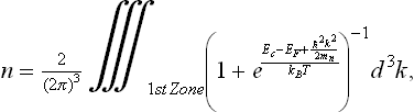
where kB is the Boltzmann constant, h is the Plank constant and T the absolute temperature.
By solving Eq. [11.1] in the case of non-degenerate semiconductors, where EF < < Ec-kBT, one obtains:
EF is the Fermi level and Nc the effective density of states in the conduction band:
which depends only on T3/2 and mn3/2.
The Fermi level is in the band gap, therefore it does not coincide with the Fermi energy (because the Fermi surface does not exist in this case), and must be identified with the electrochemical potential of the electrons.
The built-in potential, Vs (see Fig. 11.1 (a)), in the case of nanostructured polycrystalline films with grains larger than 10 nm, was measured to be of the order of 1 V (Maffeis et al., 2004) over a depletion region of about 10 nm; the resulting field is at least two orders of magnitude smaller than the atomic field, which is responsible for the band structure. Therefore, the band structure can be considered unmodified by the electrical field, and the band gap and the effective mass value can still be assumed as constant.
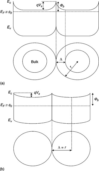
11.1 Grain boundary barrier formation in gas environment. (a) Grain radius is larger than depletion width: the bulk is reached in the core of the grain. (b) Grain radius is equal to depletion width: the grain is fully depleted and band bending starts to flatten.
Even more importantly, one is allowed to consider the semi-classical dependence of the conduction band bottom, Ec, on space coordinate x: Ec = Ec(x), thus the built-in field in the depletion region turns out to be:
The zero of energy is set in Ec in the bulk (see Madou and Morrison, 1989; Shur, 1990, pp. 140–199), i.e. far from the surface (interface between two grains, as shown in Fig. 11.1(a)). The donor states constituting the doping level, Nd, are almost all ionized at working temperatures (300–400 °C), therefore, in the bulk, n = Nd with very good approximation. Thanks to this assumption we rewrite Eq. [11.2] for the bulk of the material. Since Ec(bulk) is zero, it follows:
Eq. [11.5] is an equality between constants and can be applied to Eq. [11.2] to work out the density of electrons in the conduction band as a function of x:
With this choice of zero reference, the conduction band value at the surface coincides with q (positive value of electron charge) times Vs:
The current density in a non-degenerate semiconductor is, by applying Einstein’s relationship for diffusion and the definition of the quasi-Fermi level, EFn, to one-dimensional case:
where μn is the mobility of the majority carriers (electrons).
Therefore, the current only depends on the electrons capable of reaching the surface conduction band, i.e. those described by Eq. [11.7], and we have, by noticing that the slope of the quasi-Fermi level is proportional to the field due to the external bias along the device, Fext:
The conductivity due to the presented mechanism is then:
where σ0 = q μnNd represents the bulk conductivity. Eq. [11.10], obtained through the drift-diffusion approach, is most widely used to describe the gas sensor electrical response.
In the following, we will analyze deeply the built-in potential and the Schottky barrier formation at the intergrain interface through the mechanism of pinning of Fermi level (Malagù et al., 2004a). The case is sketched in Fig. 11.1(a),(b): a level o is defined in the gap, above which the surface states are acceptor-like (neutral when empty) and below which are donor-like (neutral when full) (Bardeen, 1947). The approximation for which gap states above EF are empty and states below are full holds, so that when EF coincides with o the surface is neutral (all donors are full and all acceptors empty). In the case of n-type semiconductors, when oxygen is being adsorbed in the form of O2− or O−, electrons of the conduction band become trapped in the surface acceptors and the conduction band bends, increasing its distance from the Fermi level (Malagù et al., 2004b). Thus, the built-in potential Vs increases and a depletion region develops whose amplitude is Λ, the depletion region width, where the electron density is very low (Fig. 11.1(a)). The position of o with respect to the Ec(surf) is constant for a given case, independent of the band bending:
The independence of band structure on band bending is assured by the observation on the field magnitude expressed above (Tersoff, 1984). At equilibrium, the surface states below EF and above o are full and acceptors, thus they constitute the negative net surface charge that compensates for the positive space charge, the density of which is Nd [m− 3]. The surface density of negatively charged states, Ns [m− 2], is given by the product of the energy density of surface states multiplied by the interval of energies where the charged surface states are present:
When the energy density of surface states Dss is very large, EF tends to o and the Schottky barrier height b (Ec(surf)-EF) becomes equal to Lo, as defined in Eq. [11.11]. This is the so-called pinning of the Fermi level, which means that the Schottky barrier is determined only by the position of the neutral level in the gap and is independent of Vs (as can be seen by comparing Fig. 11.1(a) and 11.1(b)).
For the sake of simplicity, we consider that the main adsorbed charged oxygen species is O−, so the only relevant reaction is reduced to (Sahm et al., 2006):
where S corresponds to adsorption sites at the surface, (g) refers to the gas phase, (a) to an adsorbed species and e− is an electron. Eq. [11.13] states that more oxygen in the ambient implies a larger amount of chemisorbed oxygen and thus higher intergranular barriers and lower film conductivity, as Eq. [11.10] indicates. The mechanism of Eq. [11.13] is responsible for Vs formation (band bending) as described above.
It is well established that tin oxide is a wide band-gap (3.6 eV) semiconductor in which oxygen vacancies are the dominant defects and they behave as donor impurities (Samson and Fonstad, 1973). The oxygen exchange equilibrium is regularly written as
where Vo• • is an empty ionized oxygen vacancy (Kamp et al., 2001). The corresponding mass-action law is:
Square brackets denote concentrations, K is the mass action constant, and p(O2) is oxygen partial pressure.
We are interested here in the basic mechanisms related to the dependence of surface barriers on the pressure of oxygen under equilibrium. Oxygen interstitials must be the diffusing species that alter the vacancy density in the grains of the sensing film and the mechanisms involved in the whole sensing process.
When an n-type sensor is exposed to oxygen there is a rapid increase of resistivity, indicating that equilibrium at the surface has rapidly been reached (Eqs. [11.13] and [11.10]). Then, slow resistance increase is observed, which cannot be understood without invoking another mechanism besides surface adsorption. We have explained these results as being a consequence of a decrease of vacancy density with time (Ponce et al., 2008).
For a change in donor concentration, defects constituting donors must vary, i.e. the density of oxygen vacancies must be altered. Two possible mechanisms can be proposed: first, the migration of oxygen vacancies; and second, the generation or annihilation of vacancies. At first sight, both alternatives seem to be equivalent. However, such mechanisms alter the electrical properties very differently.
In the first mechanism, charged oxygen vacancies would be mobile. Since we are dealing with charged species, oxygen vacancies could move through the solid due to a concentration gradient (diffusion) or due to an electrical field (drift). Within the depletion region there is a strong electrical field created by the ionized donors, being the oxygen vacancies themselves. Due to this electrical field, directed from the bulk to the surface, ionized oxygen vacancies would drift towards the surface irreversibly. This is not the best way to justify the experimental evidences shown here for their reversible characteristics, thus it will not be considered in this book, however the non constant doping profile along the space charge region is presently under study. Moreover, the electrical field at the depletion region is very strong to the point of sweeping the vacancies toward the grain surface, which would lead to the collapse of the intergranular barriers. It could be argued that a concentration gradient would be created and then diffusion in the opposite direction would appear. However, as discussed in detail by Romppainen and Lantto (1988), the density of oxygen vacancies under equilibrium would be orders of magnitude larger than it can physically be, close to the grain surfaces, for the normally acknowledged barrier heights, but it is consistent for lower barriers.
The second possible mechanism is the atomic oxygen diffusion in and out of the grains. Oxygen interstitials would alter the concentration of oxygen vacancies and then the intergranular barriers. Since oxygen interstitials are neutral, the electrical field at depletion regions does not affect their distributions and thus this mechanism is consistent with the reversibility observed in experiments (see section 11.4). If one used Eqs. [11.14] and [11.15] without further analysis, they would imply that the density of vacancies is inversely related to the number of electrons. If this were the case, the density of oxygen vacancies would collapse because of the electron density change across depletion regions. It has been shown that this is not the case and that, in equilibrium, the doping concentration along the grains is constant (Romppainen and Lantto, 1988).
This implies that in equilibrium the density of vacancies is independent of the n-or p-type character of the sample.
The presented findings allow us to describe the sensing mechanism in tin oxide as follows. It is assumed that temperature is such that species at grains of the sensing film can be considered in equilibrium and that the relevant bulk imperfections are anion interstitials and vacancies. The system also includes the environment where the sensor operates. If the oxygen pressure increases, the amount of adsorbed oxygen increases and the Schottky barrier height increases as well. More oxygen at the surface produces the diffusion of oxygen into the bulk as interstitials establish a new equilibrium between the surface and the bulk in which the amount of vacancies within grains is lower (Eq. [11.14]). Interstitials are mobile and neutral and vacancies are charged but once created they cannot be dragged by the field at the depletion region. (Also, as shown, the numbers of vacancies and interstitials do not depend on the number of electrons present.). When the oxygen pressure is decreased, the lack of equilibrium between the bulk and the surface provokes oxygen diffusion to the grain surface. Simultaneously, new vacancies are created and the system recovers. If the sensor does not recover, we have to consider that at least one of the processes involved is not fast enough for the system to reach equilibrium, or that the system was not originally in equilibrium. By comparing Fig. 11.1(a) and 11.1(b) one can understand that the effect of oxygen in-diffusion in a grain makes Λ increase until it reaches the value of r, the grain radius, then the bottom of the conduction band starts to be lifted and Vs decreases, but the Schottky barrier is pinned to a constant value. From the classical interpretation of thermionic conduction, explained above, conductivity would not change dramatically, since the distance of Ec(surf) from the EF stays the same. Instead, the tunneling probability of barrier crossing is shown to decrease much more. It was recently demonstrated that an interpretation relying only on thermionic effect of conductivity, normally acknowledged in the field of semiconductor gas sensing, is inaccurate as it neglects tunneling (Malagù et al., 2008).
The tunneling and thermionic contributions to the current density, normalized with respect to the flat band case, were calculated following the classical work of Crowell and Rideout (1969) for a single parabolic barrier. The whole calculation, for the double Schottky barrier at the interface (as that shown in our model; see Fig. 11.1(a), 11.1(b)), resulted in a factor of 2 in the exponent of the tunneling part of Eq. 13 in Crowell’s cited paper. Thus, the tunneling contribution, here called I1, and the thermionic one, here called I2, turned out to be:
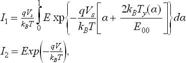
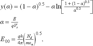
E being the energy of an electron in the conduction band and ε the permittivity; I2 is the thermionic term, representing the same behavior described in Eq. [11.10], normalized; whereas I1 depends on the shape of the barrier and not only on its height.
This model allows us to interpret all resistance variations shown in the other sections of this chapter.
11.3 Functional materials
The major requirement in developing semiconducting metal oxides for chemical sensors, and in particular thick-film gas sensing devices, is related to the control of the parameters that can affect the electrical measurements, as specified below (see e.g. Lutic et al., 2007). Besides the electronic driving of the device, the key issue is the synthesis of engineered oxide nanopowders, the functional materials. The main parameters to be controlled are the sensitivity, the lack of specificity toward the target gas and, as a consequence, the cross sensitivity, meaning that the magnitude of the response to the target gas is affected by the contemporary presence of other gases.
The sensing performance is mainly related to the surface properties (chemical, structural and morphological) of the metal oxide, and the chemistry plays a central role in tailoring its ‘receptor’ function. The chemistry is also the turning point in powder-processing to obtain sensing layers with reproducible morphology (porosity, surface geometry, size of the necks…) that take part in the gas response and transduction phenomena (Bhattacharyya and Basu, 2010).
Special attention will be devoted to the development of nanopowders with tailored characteristics via synthetic liquid–solid transformations performed under mild conditions, also called wet methods. As for any investigation concerning nanopowder synthesis, an accurate morphological, compositional and structural characterization of achieved products plays a very important role. Such studies assist the synthesis with feedback information towards the realization of a material with optimal features for gas sensing. Several specific works have dealt with this topic in the literature (see e.g. MRS Spring Meeting, 2006 and MRS Spring Meeting, 2010). Therefore, such aspects will not be treated in this chapter.
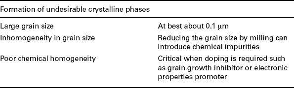
A detailed list of the parameters controlling the performance of both powders and films is shown in Table 11.2.
Table 11.2
Chemistry-controlled properties of nanopowders influencing gas sensing in the powder and processing-controlled properties of film influencing gas sensing
| In the powder | Enhancing |
| Crystalline structure | Not available |
| Particle size distribution | Narrow around the average |
| Particle morphology | Homogeneous |
| Porosity | Mesoporous (20–200 Å) |
| Purity | Pure, negligible presence of by-products |
| Specific surface area | As high as allowed by the route and kind of material |
| Stoichiometry | Oxygen vacancies Chemical homogeneity on molecular scale |
| In the film | Enhancing |
| Active surface area | As high as allowed by kind of powder and powder processing |
| Densification after firing | Low |
| Grain size | Twice the depletion width |
| Grain size distribution | Narrow around the average |
| Porosity | Mesoporous (20–200 Å) |
| Stoichiometry | Oxygen vacancies |
| Chemical homogeneity on molecular scale | |
| Texture of the film | Homogeneous, ex: absence of hill-valley effect |
| Thickness of the film | Depends on the functional material and film processing |
Chemical methods yield nanopowders with higher performing properties than the conventionally processed powders. The conventional method both for pure and multi-component powders is a solid state reaction reaching processing temperatures typically above 1000 °C. The method is not considered suitable for the synthesis of nanopowders for gas sensing because of a few disadvantages (see Table 11.3). Nanomaterials can also be produced by gas–solid processes, such as in D’Souza and Richards (2007) or in Segal (1997).
Hereafter, we provide a selection of the most well used wet methods, such as co-precipitation, and the sol-gel, hydro-thermal route, which will be described with reference to practical cases of interest.
11.3.1 Co-precipitation
Co-precipitation is used to prepare multicomponent and/or doped oxides via precursor formation, a pure or a variously complex multicomponent intermediate precipitate. The process depends on the ions in the starting materials, usually inorganic salts, precipitated by the addition of stoichiometric amounts of bases or acids. The reaction medium is usually water. The precursor is irreversibly converted into the oxide by calcination, typically performed between 400 and 900 °C. The time and temperature of the calcination belong to the chemical nature of the precursor itself and are evaluated via thermal analysis. The morphology and the specific surface area of the final oxide result as a trade-off between those two parameters. Co-precipitation allows an intimate mixing of all the desired ions in the oxide, maintaining chemical homogeneity on the molecular scale (Segal, 1997). Doping is a chance to enhance or inhibit the chemical and/or physical behavior of nanopowders whether the behavior is intentional or not. In the reaction, close attention to experimental conditions (pH, temperature, concentration) is required. Chemical homogeneity can be enhanced by sonochemical treatment with the application of ultrasound waves, ranging between 20 kHz and 10 MHz, on the reacting mixture. The resulting precursor is a function of the frequency imparted (Buzby et al., 2007). Moreover, SEM analysis assisted by Energy Dispersive Spectrometry (EDS) can be useful to control the elemental composition of small areas of certain samples.
A crucial point of co-precipitation is the kinetically driven control of the particle size and its distribution. In fact, very often the precipitation runs uncontrolled due to the difficulty in matching the suitable experimental conditions. After calcination, the nanopowder undergoes morphological and structural characterization, usually through transmission or scanning electron microscopy (TEM, SEM), specific surface area measurement by BET (Brauner, Emmett, Teller) method and finally by x-ray diffraction (XRD) analysis.
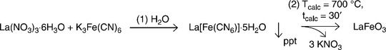
Synthesis of LaFeO3 powders
LaFeO3 is a highly nonstoichiometric ABO3 p-type semiconducting perovskite. Its catalytic properties are useful in toxic and noxious gas monitoring, such as NO2 and CO. For sensing applications, both controlled porous structure and tailored grain size are essential (see, for instance: Toan et al., 2003; Traversa et al., 1995, 1998). LaFeO3, synthesized via co-precipitation, results in nanoporous crystals with high chemical homogeneity. Figure 11.2 shows the general scheme of co-precipitation route for LaFeO3.
Synthesis of WO3 powders
WO3 powders for NO2 detection have been synthesized via precipitation. Two different routes have been compared: the choice of solvent medium is the key point for tuning both the particle size and its distribution (Guidi et al., 2004). Although each reaction starts from WCl6, the solvent exerts a restraining influence over the precursor precipitate, which leads, in turn, to different morphology of nano-oxide (see Table 11.4).
Table 11.4
Synthesis of WO3 via precipitation routes
| Reacting medium | Aqueous/surfactant | Ethanolic/dichetone |
| Starting material | WCl6 | WCl6 |
| Precursor | WO3•2H2O | Paramagnetic W(V) complex |
| Calcination | 850 °C maintained for 1 h | 850 °C maintained for 1 h |
| Grain size distribution | Bimodal | Unimodal |
| Gas sensing | NO2 | NO2 |
As highlighted in Traversa et al. (1995), for WO3 there is a wealth of nearly iso-energetic phases (Magneli phases), so that on annealing phase change occurs very easily.
11.3.2 Sol-gel synthesis method
The sol-gel route consists in the preparation of pure or multicomponent metal oxides by the hydrolysis of inorganic salts in aqueous media or metal-organic compounds in non-aqueous solutions (see for example: Segal, 1997; Buzby et al., 2007; Brinker and Scherer, 1990). A sol-gel reactive solution is a colloidal suspension (the ‘sol’), which leads to a solid and wet 3D-skeleton (the wet gel) via sol-gel transition (gelation, the ‘gel’). When the solvent is removed under atmospheric pressure, the precursor of the final oxide (the xerogel) is yielded, which is typically an hydroxide, irreversibly converted into the final oxide by calcination at temperatures between 400 and 900 °C.
During the ‘sol’ formation, the starting material undergoes hydrolysis and then condensation, or cross-condensation in the case of a route for multi-component materials. The essence of sol-gel chemistry is quite simple (Brinker and Scherer, 1990; Gopalakrishnan and Mani, 2009), but considerable efforts are still required in tuning the experimental conditions for tailoring the properties of the powders. The precise choice of both pH and concentration of the reacting mixture play a key role in driving the rate of hydrolysis and, in turn, the morphology, the specific surface area and the presence of by-products. Figure 11.3(a) shows the general scheme of the sol-gel route via inorganic salts.
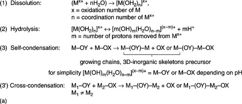
11.3 (a) General scheme of sol-gel route via inorganic salt (e.g. see Brinker and Scherer, 1990): (1) dissolution of the salt in the reacting media, the metal cations Mx + are solvated by water; (2) hydrolysis, pH-dependent process; (3) self-condensation, where for graphic simplicity [M(OH)m(H2O)n-m](x − m)+ = M–OY or M–OX depending on pH; (3′) cross-condensation in the case of the synthesis of a binary oxide where M1 ≠ M2 starting from step (1).
For the synthesis of multi-component oxides, the route proceeds essentially by the same steps, just considering the co-presence of different cations M1 ≠ M2 starting from step (1).
Metal-organics, hereinafter labeled as M(OR)n consist of a metal or a metalloid, M, directly linked with the oxygen, and R is usually an alkyl group. Sol-gel processing using metal-organics results in a better-controlled hydrolysis than processing using inorganic salts. Metal-organics are susceptible to atmospheric moisture: the M-O bonds readily react with nucleophiles so they have to be handled under inert conditions and, to avoid by-products, they could be purified before their use. Although a wide set of metal-organics is commercially available, their delicate reactivity and high cost suggest the use of an inorganic salt as starting material, or to synthesize the molecule in-situ and use it in a one-pot reaction. Figure 11.3(b) shows the general scheme of sol-gel route via metal-organic compounds.
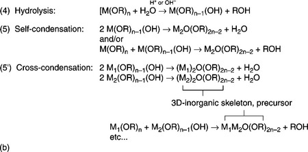
11.3 Continued (b) General scheme of sol-gel route via metalorganic compound (e.g. see Brinker and Scherer, 1990): (4) hydrolysis, acid- or base-catalyzed; (5) self-condensation; (5′) cross-condensation occurs when different alkoxides with M1 ≠ M2 are dissolved in the reaction medium. Step (5′) shows the simplest case i.e. of a binary metal oxide. There are many and complex reactions proceeding in the solution, some of which have been described in the figure. For more information see Segal, 1997, or Brinker and Scherer, 1990.
Synthesis of SnO2 and MoOx-SnO2 powders
SnO2 is one of the most gas-sensitive semiconductors for environmental monitoring, despite its poor selectivity. This property can be enhanced provided that regular morphology and narrow grain size are accomplished, or by doping. The sol-gel route via Sn-alkoxide reported in Chiorino et al. (1999) shows a good chance of achieving suitable powders for the selective detection of NO2 (see Table 11.5).
Table 11.5
Sol-gel synthesis of SnO2 via Sn(II)-alkoxide for NO2 monitoring
| Starting material | Sn(II) 2-ethylexanoate |
| Reacting medium | n-Butanol, water, HNO3 |
| Calcination | 550 °C maintained for 2 h |
| Average grain size | 20 nm |
| Grain size distribution | Unimodal |
| Specific surface area (BET method) | 31 m2/g |
| Total pore volume | 9.8•10− 2 cm3/g |
| Average pore size | 104 Å (mesopores) |
| Gas sensing | NO2 (selective) |
Synthesis of (Ti, Sn)O2 solid solutions
Extensive literature reviews the search for better sensing performance with mixed metal oxides and solid solutions when compared to single oxides, because they both have proper physical and chemical properties in respect of the pure counterparts (Radecka et al., 1998; Zakrzewska et al., 2005).
Tin dioxide and titanium dioxide are both wide-gap semiconductors, showing several similarities in structural as well as electronic properties. However, they also exhibit some peculiar differences, such as electrical conductivity and gas sensing behavior. For both materials, the n-type behavior is due to stoichiometric defects, generally oxygen vacancies acting as electronic donor levels, their energetic positions being much deeper inside the band gap for TiO2.
With respect to the synthesis procedure, in Carotta et al. (2009a) it is reported that the sol-gel route via cross-condensation is suitable for yielding a binary solid solution over the whole compositional range.
In particular focusing on the XRD characterization performed on TixSn1 − xO2 (x = 0.1, 0.2, 0.3, 0.5, 0.7, 0.9) nano-powders, the Bragg’s reflection of the (211) planes linearly shifts with titanium content between the two single oxides.
As highlighted in Carotta et al. (2009b), the proportion x = 0.2 is the boundary between tin dioxide and titanium dioxide-like behaviors in structural, electrical and spectroscopic properties.
Synthesis of ZnO powders
In Carotta et al. (2009c), zinc oxide with a unimodal grain size distribution of around 30 nm average was prepared via the sol-gel route; see Table 11.6. The films showed a good response toward O3.
11.3.3 Hydrothermal synthesis
The hydrothermal (HY) processing is ‘any heterogeneous chemical reaction in the presence of a solvent, whether aqueous or non-aqueous, above room temperature and at pressure greater than 1 atm in a closed system’ (Byrappa and Yoshimura, 2001a). The use of different solvents, or a mixture of them, helps to push down the operating pressure and favors both the solubility of the starting materials and the dispersion of the growing particles within the solvent. The reagents used in the HY processing are both inorganic and metal-organic. The precursor of the desired oxide can be synthesized via wet chemistry or via a HY route and then submitted to HY conversion into the oxide.
The equipment used for the processing is an autoclave or a ‘bomb’ (Byrappa and Yoshimura, 2001b). The technique is being extensively employed to prepare both pure single crystals and polycrystalline materials (Somiya and Roy, 2000). An important application is the synthesis of zeolites, crystalline alumino-silicates used in combination with chemical sensors to enhance their selectivity (Hugon et al., 2000; Sasaki et al., 2002). The powders prepared via HY hinder particle agglomeration yielding fine grain size down to the nanometric domain, and a narrower grain size distribution in comparison with those obtained via wet chemistry routes.
Together with SnO2, ZnO is one of the first nanomaterials studied for thick-film gas sensing devices. Because of its poor selectivity and high working temperature (400–500 °C), over the years it has become gradually less popular, favoring the study of more promising materials. With emerging powders processing applied in the field of nanoceramics, such as the HY technique, ZnO has been reconsidered with the aim of improving its performances by tailoring, for example, its morphology (Baruwati et al., 2006; Asamoto and Yahiro, 2009).
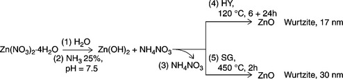
Hydrothermal synthesis of ZnO
In Baruwati et al. (2006), ZnO nanoparticles are synthesized in double distilled water, at 120 °C using an autoclave, showing that HY treatment hinders the ZnO grain growth when compared with ZnO synthesized via the sol-gel route starting from the same reacting conditions (Carotta et al., 2009c), see Table 11.7 and Fig 11.4.
Table 11.7
Comparison between the sol-gel (SG) and the hydrothermal (HY) synthesis of ZnO
| Process | SG (3.14) | HY (3.20) |
| Starting material | Zn(NO3)2•4H2O | Zn(NO3)2•4H2O |
| Medium | Doubly distilled water | Doubly distilled water |
| Catalysis | NH3, pH = 7.5 | NH3, pH = 7.5 |
| Precursor | Zn(OH)2 | Zn(OH)2 |
| Processing conditions | Calcination 450 °C for 2 h | HY 120 °C for 6 ÷ 24 h |
| Crystal structure | Wurtzite | Wurtzite |
| Average crystallite size | 30 nm | 17 nm |
| Gas sensing | Oxidizing gases (O3) | Reducing gases (LPG, EtOH) |
Hydrothermal synthesis of monodispersed perovskite powders
Perovskite-type nanopowders are performing materials for gas sensing devices considering their catalytic behavior (Asamoto and Yahiro, 2009). In Ding et al. (2001), the morphology and structure of perovskites are tailored with HY processing obtaining optimal chemical homogeneity. Details of the synthesis are reported in the Fig. 11.5
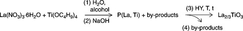
11.5 Chemical equation representing the HY synthetic route for lanthanum titanate nanopowders. The label P(La,Ti) corresponds to the precursor of the Þnal powder whose stoichiometry has been not reported in the literature. The by-products (alcohols, unreacted starting materials and undesired oxides) have been separated from La2/3TiO3 after HY treatment.
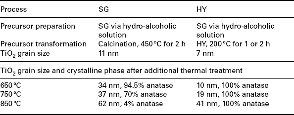
Comparison between titania thick-films obtained through sol-gel and hydrothermal synthetic processes
TiO2 nanopowders are used in thick-film gas sensors for reducing gases. Material calcined above 600 °C undergoes phase transition from anatase into rutile leading to grain growth and coalescence, reducing its sensitivity toward the environmental changes. In sol-gel processing the morphology of titania is driven by calcination performed on the precursor.
In Carotta et al. (2007a), anatase is maintained also after a thermal treatment performed at 850 °C when the precursor has been previously submitted to a HY treatment. A comparison between the results gained in both experiments is reported in Table 11.8.
11.3.4 Rheology, pastes and screen-printing technology
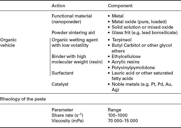
The study of compressing and deforming strengths on a system is the base of rheology, which is crucial to selecting the methodology and the equipment for mass processing the powder. Thick-films are fabricated from printable pastes of functional materials in the form of powder, inorganic additives and organic binders. The structure of a paste easily changes with time, temperature and shear stress. Its physical characteristics depend on all components added to the paste and their interactions (Reed, 1995a). Moreover, the pastes for screen-printing must be thixotropic: during the printing processing, the viscosity of the paste must decrease under an applied shear stress and increase when the stress is removed (Reed, 1995b).
The viscosity of the paste depends on the loading in powder, resins and solvents percentage. Resins dissolved in the solvents yield the organic vehicle, whose viscosity affects that of the paste. The most common formulation for screen-printable paste is listed in Table 11.9; specific paste compositions are highly proprietary.
In screen-printing technology a patterned woven mesh screen defines the pattern to be printed onto a substrate by a squeegee, a polymeric blade whose stiffness is chosen according to the process to be carried out. The screen is a set of regularly spaced woven mesh anchored on a rigid frame, under calibrated-tension conditions.
The caliber and type of the cables depend on the detail required for the pattern, the rheology of the paste, shape and roughness of the substrate and the thickness of the final layer. To print a layer with a specific pattern, the paste must flow only through the empty areas of the screen; each printed block will merge into a compact film.
The variables influencing the printing processes are listed in Table 11.10. For both the best pattern resolution and the best printing quality, a trade-off between all the tabulated parameters is a must.
After printing, drying allows the removal of the volatile components from the paste (100–200 °C) (Reed, 1995c).
Shrinkage occurs when the liquid between the solid particles is removed and inter-particle separation decreases; this effect can be reduced when the grain size distribution of the powder is spread over a wide dimensional range. Drying is the step prior to firing, the thermal process that imparts and consolidates the shape of the printed layer, and also develops its microstructure and properties. Unfired ceramics are weak and can sustain only weak stresses without deformation or local fracture. Firing is performed in furnaces under ambient atmosphere between 600 and 1000 °C. The oxygen partial pressure drives the content of metals or metalloids with the proper oxidation state, in the functional material; rarely, some layers need to be treated in a different atmosphere to tailor the stoichiometry of the material itself.
Firing proceeds in three steps: (1) organics burnout and gaseous by-products elimination; (2) sintering; and (3) cooling (Reed, 1995d).
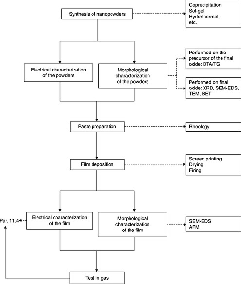
The glass frit, in the paste formulation, is essential to improve the adhesion of the printed film onto the substrate. During sintering it achieves its softening point, turning from a solid to a viscous glassy matrix wetting the grains uniformly. The matrix draws the particles together enabling their sliding and rearrangement into a denser configuration. Rarely more than 1% w/w of glass frit, with respect to the weight of the powder, is required to coat entirely the grains at the softening point. When the frit is inhomogeneously distributed within the paste, different rates of densification and grain growth may cause inhomogeneous microstructure and a low average density of the resulting film. In Fig. 11.6 the flow chart of the total process is shown.
11.4 Morphological, structural and electrical properties
As highlighted in the previous section, among the most interesting materials for gas sensing, SnO2, TiO2, WO3, ZnO, pure or modified with ion-addition or catalysts are certainly very common.
This section aims to analyze the electrical properties of thick-film gas sensors prepared through the above functional materials, focusing on the peculiar characteristics of each of them.
The interest in wide-gap semiconductor oxides began in the 1960s, when Seiyama et al. (1962) discovered their peculiarity of modifying surface properties when interacting with reducing or oxidizing gases. Over the years, a lot of studies have been addressed to improve the sensitivity and selectivity properties of chemo-resistive gas sensors, while probably neglecting the study of factors affecting the repeatability. However, of the various types of metal oxide gas sensors, thick-film gas sensors are surely the most reliable. Indeed, as shown in Fig. 11.7, in which the carbon monoxide concentration was alternately changed between 5 and 40 ppm, the sensor response was quite repeatable.
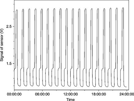
11.7 Alternate response of a SnO2-based thick-film sensor to 5 and 40 ppm CO. The duration of a whole response is 1 h, the duty cycle is 50%.
11.4.1 SnO2-based materials
Among the above-mentioned materials, a case in point is tin dioxide, the most widely used material for gas sensing, by which in 1970 Figaro Engineering Inc. fabricated and commercialized the first metal oxide gas sensor device (Taguchi, 1970). SnO2 exhibits n-type semiconductor behavior due to lattice defects, in particular oxygen vacancies acting as electronic donor levels. Indeed, Samson and Fonstad (1973) experimentally determined the presence of two donor levels, Ed1 = 0.034 and Ed2 = 0.145 eV below the bottom of the conduction band.
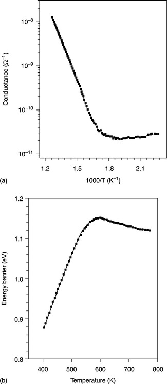
Figure 11.8 shows the Arrhenius plot obtained by changing the temperature between 360 and 800 K at the heating rate of 3 K/min (A) and the height of the surface barrier potential versus temperature (B) of a SnO2 thick-film. To determine the energy barrier (the difference in energy between the conduction band bottom at the surface and that in the bulk) temperature-stimulated conductance measurements were performed with a procedure described elsewhere (Lantto et al., 1988; Carotta et al., 1991).
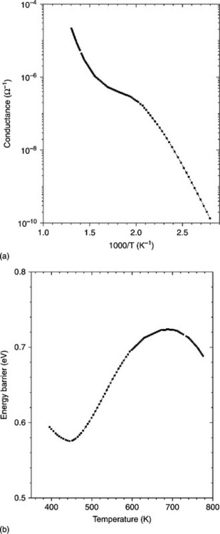
11.8 Arrhenius plot for (a) conductance and (b) energy barrier vs. temperature, for pure tin oxide films.
Different conductivity regions were observed, demonstrating the occurrence of different surface adsorption phenomena, in particular the O2− – O− transformation, as experimentally proven by Chang through the correlation between electrical conductivity and EPR measurements (Chang, 1980). The typical behaviour of the SnO2 energy barrier versus temperature exhibits a minimum and a maximum corresponding to the increase of the depletion layer depth with temperature attributed to a negative surface charge accumulation, typically O− ions. The ability of tin dioxide to sense either reducing agents at high temperature or oxidizing ones, like NO2, at low temperature could be explained according to these characteristics. The interaction between the analyte and the surface of the semiconductor causes changes to the potential barrier height at the inter-granular contact and therefore to electrical conductance variations.
All the electrical measurements here shown have been obtained in a sealed test chamber using the flow-through technique maintaining a constant flow of 0.5 l/min in dry or wet air or in mixtures of air and test gases.
As the first material extensively investigated in gas sensing, many studies have been performed to improve the sensing and selectivity properties of SnO2, above all by adding small amounts of noble metals on the surface (Yamazoe et al., 1983; Schierbaum et al., 1991; Yamazoe, 1991; Fliegel et al., 1994; Xu et al., 1996; Cabot et al., 2000, 2002). On this subject, in Batzill and Diebold (2005) the role of additives in gas-sensing materials has been thoroughly reviewed. In Chiorino et al. (1997), the role of Pd has been examined on two materials, a commercial SnO2 powder from CERAC and a SnO2 powder prepared in the laboratory by a precipitation route, differing in grain size and the shape of grains. It turned out that the role of the nanostructure associated with a high dispersion of small additive particles resulted in a higher gas response and reduction of the operating temperature. Figure 11.9(a) shows a result of TEM investigations performed on powders calcined at 550 °C and on films loaded with 0.4 at.% of Pd and heated up to 850 °C (Fig. 11.9(b)). The round-shaped particles exhibit an average diameter of 20 nm, a little wider (< 30 nm) in the films.
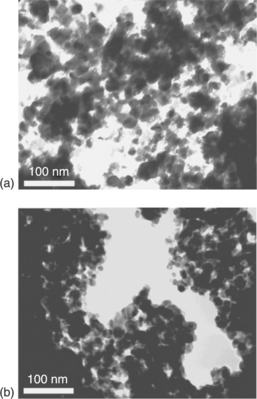
11.9 (a) TEM micrographs on to SnO2 powder calcined at 550 °C and (b) onto Pd/SnO2 film fired at 850 °C.
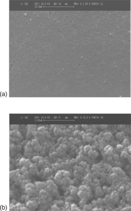
Moreover, in Fig. 11.10, the SEM micrographs performed on Pd-loaded films show the crack-free film surface (Fig. 11.10(a)) and the optimum degree of particle sintering control (Fig. 11.10(b)).
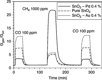
From the electrical point of view, Fig. 11.11 illustrates the different sensing effect of Pd or Au (0.4 at.%) addition on the detection of carbon monoxide and methane.
Fourier-transform-infrared-spectroscopy (FT-IR) measurements enabled us to clarify the role of the oxygen vacancies for the laboratory-prepared material. Indeed, in the presence of reducing gases, a growth of a very intense and broad absorption peak due to electronic transitions involving oxygen vacancies appeared, which is not present in the commercial powder. On the contrary, for the latter material, only an increase of the scattering of the radiation by free electrons could be found, thus highlighting the difference between a nanostructured material and a coarser one and the importance of a high stoichiometric defectiveness of the sensing material associated with the nanostructure.
Other selectivity properties can be obtained by adding different ions to SnO2 crystal lattice, such as Mo, W, V, La, etc. The addition of Mo and W generally resulted in a decrease of the response to reducing gases, like CO, and in an increase versus oxidizing gases, such as NO2, while for V and La addition, a good sensitivity to SO2 and CO2, respectively, is reported (Chiorino et al., 1999, 2001; Das et al., 2008; Marsal et al., 2003).
As stated above, the synthesis method involves different electronic properties, while the decrease in grain dimension down to the depletion width provides an enhanced gas response (Malagù et al., 2004a, 2004b; Xu et al., 1991; Vuong et al., 2005; Zhang and Liu, 2000). Actually, in tin oxide thick-film sensors it is unusual to observe the grain size dependence of the response. Indeed, the firing at high temperature causes a grain coalescence of up to 20–30 nm. Because the depletion layer depth in tin oxide is less than 20 nm, in order to observe this phenomenon the sensing layers must be deposited starting from very small powders (< 10 nm) and heated at a moderate temperature (≤ 650 °C) (Malagù et al., 2004c). Under these conditions, we have experimentally verified that the response to carbon monoxide doubles when the grain size is about 10 nm with respect to that of a grain size of about 30 nm.
In spite of the many improvements obtained through material modifications (such as the synthesis of nanostructured powders and the addition of ions or catalysts), a significant cross-sensitivity caused by the presence of a small amount of water vapor greatly hindered the exploitation of tin oxide-based gas sensor devices. Several authors visited the subject following different approaches: first of all by studying the mechanism of interaction between the semiconductor surface, detecting gas and water vapor and afterwards trying to solve the drawback through material modification, filters or processing the sensor signal by mathematical algorithms. Some papers on this subject are listed: Yamazoe et al., 1979; McAleer et al., 1988; Gercher and Cox, 1995; Ghiotti et al., 1997; Bârsan and Weimar, 2003; Harbeck et al., 2003; Marsal et al., 2003; Ankara et al., 2004; Ivanov et al., 2004; Hossein-Babaei and Ghafarinia, 2010. In particular, in Carotta et al. (2007b), a compensation algorithm has been obtained through experimental tests and positively applied to the monitoring of atmospheric pollutants. The resulting equation, which represents a surface, contains three terms: two of them represent the response to a single gas and the third one is an interaction term between the water vapor and the testing gas.
11.4.2 TiO2-based materials
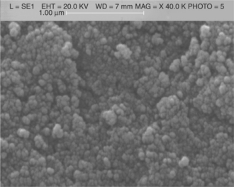
Among the large variety of TiO2 applications, the photo-assisted degradation of organic molecules is certainly the most exploited. So, the major knowledge of titania as a functional material comes from catalysis and photocatalysis (Fujishima and Honda, 1972; Matsuda and Kato, 1983; Linsebigler et al., 1995; Paz, 2010; Diebold, 2003). In the gas sensing field, titania was first investigated for its application in automotive exhaust sensors, i.e. in the measurement of the oxygen partial pressure in the exhaust gas, and hence for the control of the air/fuel ratio (Tien et al., 1975; Takami, 1988; Zhu et al., 1996; Sharma et al., 1996). Since the 1990s, titania has been studied to detect atmospheric pollutants at moderate temperature (300–600 °C) (Tang et al., 1995). Actually, titania is suitable for sensing polluting gases in air, allowing good and stable responses only if the grain dimension of the poly-crystalline material is kept at nanometric level. Indeed, in contrast to SnO2, titanium dioxide, when heated, undergoes a phase transition from anatase into rutile, simultaneously resulting in very large grain coalescence (Hague and Mayo, 1993; Guidi et al., 2003). The anatase phase can be stabilized through the addition of ions with valence 5+ (Guidi et al., 2003; Akhtar et al., 1992; Martinelli et al., 1999; Carotta et al., 1999; Traversa et al., 2001; Ruiz et al., 2004a; Sacerdoti et al., 2004). In particular, Ta (10 at. %) allowed to hinder the transition to rutile up to 950 °C (Traversa et al., 2001). A different method of stabilizing titania in the anatase phase consists of synthesizing the oxide by using the sol-gel route (SG) followed by an appropriate treatment HY (Ruiz et al., 2004b; Carotta et al., 2007a). In contrast to the traditional SG synthesis, the HY process allows for the maintenance of the anatase phase up to 850 °C without any introduction of foreign elements (Carotta et al., 2007a). In Fig. 11.12, a SEM image of a HY–titania thick-film fired at 850 °C shows nanosized particles with an anatase structure as confirmed by XRD analysis.
In spite of the excellent results in terms of anatase phase stabilization with the consequent maintenance of the grain dimension at nanometric size, the TiO2-based gas sensors differ in gas-sensing behavior from SnO2-based ones, the latter being much more reactive versus reducing gases. A theoretical model has been developed to justify this behavior. The idea was to generalize the Schottky relation (Morrison, 1982) to the case of spherical symmetry and to the cases where the depletion approximation fails. The result is a strong grain-size dependence of the TiO2 gas-sensing properties caused by the variation of the charged surface states, Ns, with grain radius. SnO2, instead, exhibits a modest dependence of the gas response on the particle size (as confirmed by experimental evidence) due to an almost constancy of Ns (see section 11.2).
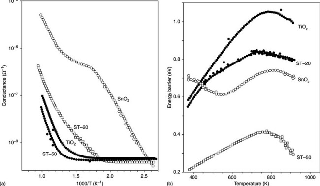
TiO2 strongly differs from SnO2 in that it has a much smaller electrical conductivity and the shape of the Arrhenius plot is different (see Fig. 11.13(a)). Indeed, the sigma shape caused in SnO2 by the occurrence of surface reactions (in particular the O2−–O− transformation in the 200–400 °C range) is not visible in TiO2 because in this temperature range the bulk donor states are not yet ionized. In fact, the n-type behavior, in TiO2, as with SnO2, depends on donor-like stoichiometric defects, generally ascribed to oxygen vacancies, but with energetic positions in TiO2 that are much deeper inside the band gap with respect to SnO2 (Samson and Fonstad, 1973; Munnix and Schmeits, 1985). Actually some authors assign donor levels 0.8 eV deep, at Ti3 + ions rather than at oxygen vacancies (Diebold, 2003; Göpel et al., 1988). Moreover, titania films feature heights of energy barriers versus temperature that are much higher than SnO2, where almost three activation energies are exhibited, differently from TiO2, in which only two regions of barrier are present (see Fig. 11.13(b)).
11.13 Arrhenius plot for (a) conductance and (b) energy barrier vs. temperature for pure titania films.
With respect to the structural properties, SnO2 and TiO2 exhibit the same rutile crystalline structure, the space group P42/mnm easily giving rise to a solid solution with chemico-physical properties varying with the Ti–Sn molar ratio. In fact, the SnO2-TiO2 system has been widely investigated; in some of the papers mentioned here, the characteristics of the immiscibility gap can be found (Park et al., 1975; Yuan and Virkar, 1988; Radecka et al., 1998; Dusastre and Williams, 1999; Radecka et al., 2001). Actually, the SnO2-TiO2 mixed oxide is a very interesting material for thick-film gas sensors and its synthesis and investigation (as TixSn1-xO2, 0 < x < 1 with x = 0, 0.1, 0.2, 0.3, 0.5, 0.7, 0.9, 1) allowed us to discover a completely different phenomenon occurring during the sensing process in SnO2-like materials compared with what happens in TiO2-like ones. Indeed, through FT-IR analysis under a CO atmosphere, for the materials with x ≤ 0.2, as already observed in pure SnO2 (Chiorino et al., 1997), a very broad absorption in the medium IR (MIR) region, related to the photoionization of mono-ionized oxygen vacancies VO., occurred, while samples with 0.3 ≤ x ≤ 1 exhibited a completely different phenomenon consisting in an erosion of the absorption edge related to the skeletal M–O vibration modes (Carotta et al., 2009b). This difference of behavior can contribute, together with the definition of the phenomenon of the unpinning of the Fermi level (Malagù et al., 2004b; Carotta et al., 2007a) to understanding the electrical differences between SnO2 and TiO2.
In summary, with regard to the electrical properties of the various solid solutions obtained by varying the Ti molar ratio, all examined samples with 0.1 ≤ x ≤ 0.9 exhibit good sensing performance, even if they exhibit a crystalline rutile structure. However, it must be noted that these materials do not undergo a phase transformation, exhibiting a rutile phase as synthesized. For this reason, the grains undergo coalescence only moderately when heated at high temperature. In Fig. 11.14(a), the crystallite dimension of the powders calcined at 650 °C, estimated through XRD analysis using Scherrer’s equation, is reported, whereas that of pure titania is not reported because at 650 °C the crystalline phase is anatase instead of rutile. In Fig. 11.14(b), the response to 50 ppm of carbon monoxide (working temperature: 550 °C) of the thick-films fired at 650 °C, as a function of the crystallite size of the films, is shown. We note that the crystallite size is strongly dependent on composition, exhibiting the lowest size for 0.3 ≤ x ≤ 0.5, while the gas response increases with decreasing grain size rather than with the Ti molar ratio, as might have been supposed (Carotta et al., 2008, 2009a, 2009b).
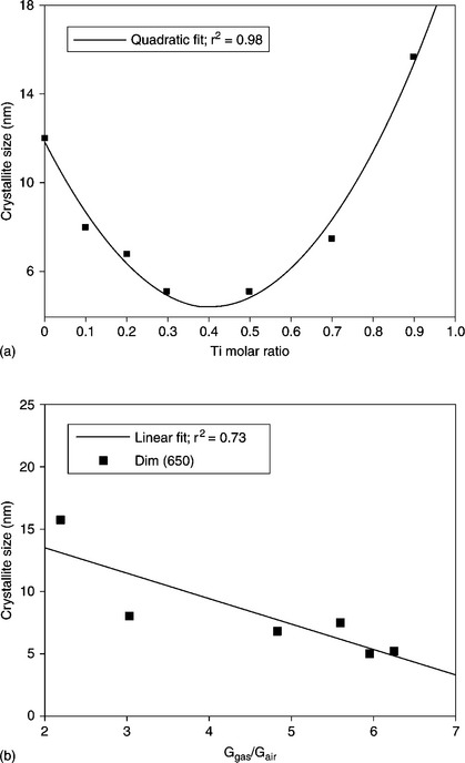
11.14 Crystallite size of (Sn,Ti)-solid solution powders vs. (a) Ti molar ratio and (b) magnitude of the response for (Sn,Ti)-mixed oxide films fired at 650 °C as a function of crystallite size.
From the electrical point of view, the materials with x ≤ 0.2 exhibit conductivity much higher than the compositions with x > 0.2; the two classes of materials also show different shapes of conductance curve versus temperature (Carotta et al., 2009b). Concerning surface barrier height trend versus temperature, the sample with x = 0.1 behaves similarly to SnO2 with an increased barrier height corresponding to the decreased conductivity. The samples with 0.3 ≤ x ≤ 0.9 behave like titania (temperature dependence), but the height of the energy barrier was determined by the size of the nanoparticles. Indeed, the grain radius of the samples with x = 0.3 and x = 0.5 are smaller than Λ (the depletion layer width) and the band bending cannot be fully developed (Carotta et al., 2009a, 2009b). In summary, among the various synthesized TixSn1 − xO2 solid solutions, the stoichiometry with x = 0.2 exhibits a borderline behavior between that SnO2-like and TiO2-like oxides, for all examined properties (see Figs. 11.15(a), 11.15(b)).
11.4.3 WO3-based materials
Tungsten trioxide has been investigated mainly because of its wide number of crystalline forms, in contrast to its simple stoichiometry (Boulova and Lucazeau, 2002; Vogt et al., 1999; Howard et al., 2002). Since then it has been appreciated in many applications and mainly in electrochromic devices (Jiao et al., 2010; Kharade et al., 2010), photo-catalysis under UV and visible light (Bamwenda and Arakawa, 2001; Kim et al., 2010) and, especially from the 1990s, in gas sensing (Akiyama et al., 1991; Tamaki et al., 1994; Tomchenko et al., 1999; Lee et al., 1999; Solis et al., 2001; Guidi et al., 2004; Kanda and Maekawa, 2005; Reyes et al., 2006; Meng et al., 2009; Szilágyi et al., 2010; Senguttuvana et al., 2010). Regarding this application, WO3 appears mainly investigated in NO and NO2 sensing. Also H2S and ammonia have been considered, but very few papers assess the capacity of WO3 to detect reducing gases, like VOC or hydrocarbons. According to the majority of the authors, the WO3 thick-films prepared by our group exhibit a strong attitude to oxidizing gases (Guidi et al., 2004; Blo et al., 2004).
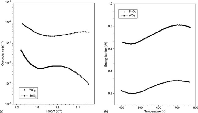
Like SnO2, WO3 behaves as a n-type semiconductor because of latttice defects, in particular, oxygen vacancies acting as electronic donor levels. However, it shows a band gap ranging from 2.5 to 2.8 eV (Erbs et al., 1984) and contemporaneously a conductance value, at low temperature, almost three orders of magnitude higher than SnO2 (Fig. 11.16(a)). Both materials exhibit three regions of conductance and therefore the same trend versus temperature of the surface energy barrier, but with a very low value in the case of WO3 (Fig. 11.16(b)). This fact could explain the ability of WO3 to detect only oxidizing gases.
Also the preparation of mixed oxides of tungsten and tin tends to exhibit the same behaviour in relation to oxidizing gases. Indeed, as shown in Chiorino et al. (2001), adding 1 or 5% of W in SnO2 progressively modifies the sensing properties of the sensors from the detection of reducing to the detection of oxidizing gases. Furthermore, the solid solution of (Sn,W)O3 (Sn: 10 at.%) did not increase the ability of the mixed oxide with respect to pure WO3 to detect oxidizing gases (Fig. 11.17).
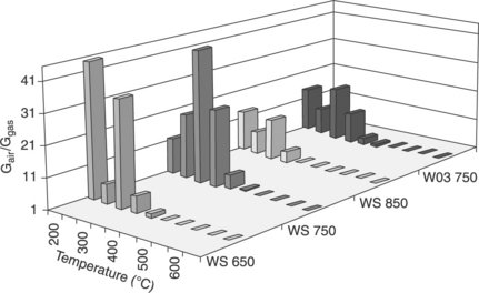
11.17 Magnitude of the response to 100 ppb of NO2 for pure WO 3 sensor fired at 750 °C compared with those offered by (Sn,W)O3 (Sn: 10 at.%) films fired at 650, 750 or 850 °C.
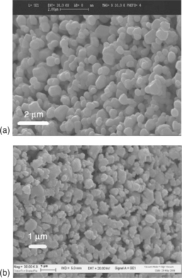
Under thermal treatment, WO3 suffers from exaggerated grain coalescence assisted by phase transition as highlighted in Guidi et al. (2004) and shown in Fig. 11.18, in which a pure WO3 film (a) is compared with a film of (Sn,W)O3 (Sn: 10 at.%) (b), both fired at 750 °C. Moreover, it has been proved that NO2 response depends on particle size (Guidi et al., 2004; Meng et al., 2009), but the phenomenon becomes significant only if the grain size is very small (< 30 nm) as reported in Tamaki et al. (1994). Unfortunately, to obtain a good electrical stability of the sensors, it is essential to operate them at a sufficiently high temperature. For this reason, specifically for WO3, particles smaller than 30 nm are not consistent with the manufacturing process. On the other hand, responses to other oxidizing gases, like ozone, are quite independent of particle size, therefore, for WO3, it does not appear clear if the gas response might even depend on gas molecule size and gas diffusion effect.
11.4.4 ZnO-based materials
ZnO has been a pioneering material in gas sensing (Seiyama et al., 1962). Later it was abandoned, but in the past two decades it has again met the interest of researchers as witnessed by an exponential growth of publications. Zinc oxide is a direct wide band-gap (3.37 eV) semiconductor and exhibits high exciton binding energy (60 meV), which causes an efficient UV emission (~ 380 nm), making it suitable for UV- and blue-optoelectronic applications. Furthermore, a wide range of other technological applications such as photocatalysis, piezoelectricity, optoelectronics, photovoltaic conversion and gas sensing make ZnO a very attractive material (Özgür et al., 2005; Klingshirn, 2007; Ruske et al., 2007; Dodd et al., 2009; Martins et al., 2004). With the advent of modern nanotechnologies, a lot of metal oxide semiconductors have been synthesized in a large variety of nanostructures such as nanoparticles, nanowires, nanobelts, nanorods or nanotetrapods. Among the various oxides, ZnO is particularly suitable to be synthesized in such nano-forms (Schmidt-Mende et al., 2007; Wang, 2004). In this context, recent works in gas sensing claim the superior performance of two-dimensional nano-morphologies with respect to traditional round-shaped three-dimensional nanoparticles (Schmidt-Mende et al., 2007; Wang, 2004; Lu et al., 2006). In Carotta et al. (2009c), a comparison between round-shaped and two-dimensional nanoparticles in the form of tetrapods (TP) has been performed. It turned out that, despite the enormous difference in morphology, both types of sensors behaved similarly with all tested gases, mainly exhibiting very good responses towards oxidizing gases, in particular with ozone. TP films best responded to ozone with faster response time, while sol-gel thick-films best responded to NO2 with a different temperature of maximum response compared to ozone.
ZnO has been successfully employed also to detect other gases, such as H2, O2, H2S, LPG, HCHO and NH3 (Patil et al., 2010; Baruwati et al., 2006; Trivikrama Rao and Tarakarama Rao, 1999; Sarala et al., 2006; Xiangfeng et al., 2005). In addition to thermally activated gas sensors, ZnO is particularly suitable to be assisted by UV irradiation. In this operational mode, the sensors work at room temperature overcoming the main technical limitation of the high operating temperature, essential in chemo-resistive gas sensors. Actually, the photoactivation has been investigated for other metal oxide semiconductors, such as, for example, SnO2 or TiO2 (Prades et al., 2009; Yan et al., 2010; Yang et al., 2003). However, ZnO is the most investigated material with UV light instead of thermal energy as the excitation source (de Lacy Costello et al., 2008; Gui et al., 2008). Our group successfully applied the gas detection assisted by an UV light-emitting diode (LED) to ZnO sensors for ozone detection (Carotta et al., 2011); for this application (see also the next section), the most appropriate morphology has been obtained by firing the sensing film at 650 °C (see Fig. 11.19).
11.5 Applications
Over the years, the wide variety of technological applications, such as heterogeneous catalysis, gas sensing, photocatalysis, piezoelectricity, optoelectronics, photovoltaic conversion, etc. has been driven by extensive investigations on semiconductor metal oxides (MOX). To use them in real applications, many efforts have been addressed to improving their selectivity and repeatability properties, which still represent the main drawback for a single sensor employment. However, the crucial point is to prioritize the identification of the specific application, in order to reduce as much as possible the number of parameters that can influence the measurement. In the following, we will describe the applications to which we have devoted major attention in order to minimize the above expressed problems or to solve them either by using on array of sensors or with dedicated analytical methods.
11.5.1 Environmental monitoring
The worldwide emission of pollutant gases and fine particulate matter caused by vehicular traffic, industrial activities, domestic heating and biomass burning is steadily increasing. In particular, emerging industrial activity in developing countries will further add to the global pollution during the next decades. Increasing concerns for the proven impact of atmospheric pollution on the health of citizens strengthens the necessity of emission control and mitigation, which have to be verified through steady public and private air quality monitoring activities.
Recent developments in the European legislation have enabled proposals for the use of more flexible devices, such as reliable solid-state gas sensors, in addition to cumbersome analytical devices (Commission Directive 2008/50/EC). Indeed, real-time in-situ air quality data acquisition is necessary for assessing pollution, but also as an input for pollutant diffusion models and for the validation and correlation with remote sensing measurements. Nowadays, monitoring is usually performed in few fixed stations in urban areas, and with mobile stations (where the conventional equipment is installed on vehicles) for temporary measurement campaigns or occasional environmental impact estimations. The equipment used in these stations is often complex, expensive and difficult to deploy, requiring controlled environmental conditions and frequent maintenance and calibration. These analyzers are mainly rack-mounted devices with several requirements like external gas cylinders, consumables and periodic fetching and processing of the acquired data by trained personnel.
In this frame, the technology of thick-film gas sensors is an optimal candidate to be implemented in portable devices with low requirements in terms of power, consumables, maintenance and installation costs. Besides an evident cost reduction, this implementation will enable on-board correlation and processing of the acquired data, which can be autonomously distributed in a user-friendly format via the integrated wireless network interfaces and/or radio-modems (Qi and Shimamoto, 2012).
The advanced thick-film gas sensors are prepared as described in section 11.3 with optimal levels of reliability, stability, reproducibility and response speed for the different target gases, such as CO, NOx and O3. These sensors are used to monitor the air quality with sensitivity, selectivity and reliability comparable to that of conventional analytical devices. In Fig. 11.20 both the sensor components of the system and the assembled monitoring unit are reported.
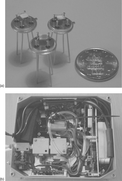
11.20 (a) Photograph of the single sensors of Fig. 11.20(b); (b) prototypal monitoring unit endowed with two sensor test chambers, flow and electronic control systems.
Figure 11.21 shows a comparison between dynamic measurements of (a) CO, (b) NOx and (c) O3 performed through the described system with those of conventional spectrophotometers, while in Fig. 11.22 the correlation between the results of the two instrumentation is reported for the case of ozone.
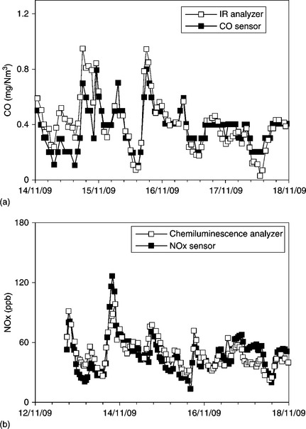
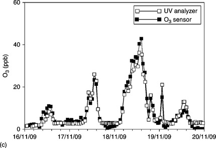
11.21 Dynamic measurements of different gases compared with conventional analyzers (a) CO and (b) NOx. (c) O3.
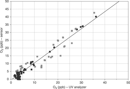
The sensors shown in Fig. 11.20 can also be employed inside a gas chromatograph or in an array controlled by suitable electronics; therefore, they fit perfectly a scenario in which integrating measurements of outdoor pollutants are performed, from both fixed and mobile web-enabled stations. In this context, an integrated system realized in collaboration with CNR-IMM is sketched in Fig. 11.23.
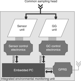
The integrated innovative system performs detection and quantification of atmospheric pollutants, in particular carbon monoxide, nitrogen oxides, ozone and aromatic volatiles. Details about monitoring gaseous pollutants in the atmosphere using semiconductor sensors as detectors can be found, e.g. in Viricelle et al., 2006; Zampolli et al., 2009; Carotta et al., 2006. The employment of this system on city buses together with geostatistic modelling results in the reconstruction of spatial distribution of pollutants in the area of interest. The system was tested in the year 2010 in the frame of GEOBUS, an Emilia Romagna PRRIITT Programme, a result of which was a picture of the distribution map of the carbon monoxide in a certain area of Bologna.
11.5.2 Photoactivation and photocatalysis
The wide-ranging features of MOX sensors also promoted research into photonic applications, such as light-emitting or laser diodes, transparent conducting oxides (TCO), hybrid solar cells, and material photo-activation and photocatalysis. Moreover, the recent emphasis given to the research on nanostructures and the advent of modern nanotechnologies has opened the way to further improvement in this direction.
In particular, in the case of nanostructured metal oxides used as gas sensors, many studies on exposure to light have been performed (Rao and Rao, 1999; Izu et al., 2004). The basic idea arises from the fact that some metal oxides, known for their good sensing capabilities, also show photocatalytic properties, the photo-generated carriers promoting chemical reactions with the adsorbed species on the semiconductor surface.
The mechanism mainly involved in the described application, is the following: given that the absorption of a photon with enough energy promotes an electron in the conduction band and it generates a hole in the valence band, two specific mechanisms can contribute to the phenomenon: (1) the photo-generated holes recombine with electrons trapped on the surface causing desorption of the adsorbed oxygen ions. This results in a conductivity increase, due to the increased free electron density; (2) since the sensing layer is nanocrystalline, it is reasonable that many of the electron–hole pairs are generated within the depletion region causing a decrease in the energy barrier height.
An experimental result in this frame consisted in the observation that, under UV irradiation, the conductivity of ZnO increased by two orders of magnitude in ZnO. An important application, as reported in Chapter 4, is a ZnO ozone sensor exhibiting excellent performance in sensitivity, in response and recovery times also at room temperature (see Fig. 11.24). This result finds its application both in particularly harsh environments, e.g. in factories and plants where explosives may be present, and in situations where a very low power supply is required.
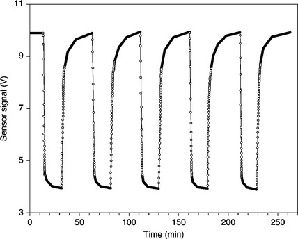
In the same context, a novel employment of nanostructured metal oxides has been tested by our group consisting in monitoring the photoactivity of functionalized tiles for atmospheric pollution abatement, as can be observed in Fig. 11.25, in which a test of abatement of 2 ppm of NO is monitored through two sensors, one based on ZnO and the second one based on (Sn,W)O3 (Sn: 10 at.%). The opposite response of the two sensors is caused by the contemporaneous presence of NO and NO2 in the atmosphere induced by operating functionalized tiles.
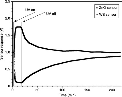
11.6 Future trends
The encouraging results achieved with previous applications foster further improvement for the industrialization of innovative instrumentation to access the market. Indeed, at present, it is only possible to acquire expensive instrumentation, generally cumbersome and of a laboratory type, which makes its widespread diffusion very difficult.
In the case of environmental monitoring, the proposed instrumentation, due to its portability and low cost, can instead offer the possibility of enhancing the capacity to protect the population from air pollution and assess health risks. It can also enable on-board correlation and processing of the acquired data to be autonomously distributed via the integrated wired and wireless network interfaces.
Sensor-based monitoring is highly portable and user-friendly so as to grab the attention or solve the problems of specific fringes of society (such as children, the elderly, people exposed to work hazards), because it allows the user to check real-time data about air quality, such as ozone concentration in urban parks during the summer season or benzene concentration in petrol stations, and so on.
In the case of the other applications described in section 11.5, the enhanced performance features such as portability and the other described characteristics can result in sustainable development, from both the technical and the economic points of view, with subsequent potential social impact.
11.7 Acknowledgments
We are very grateful to Professor Giuliano Martinelli, head of our laboratory from 1995 to 2010, for passing on his love of and enthusiasm for research to us.
The results reviewed in this paper have been obtained with the help of members of our group (in particular, Michele Benetti, Sandro Gherardi, Alessio Giberti, Marco Nagliati, Daniela Palmeri) and eminent scientists of other institutions: Gian Carlo Cardinali, Stefano Zampolli, Giovanna Ghiotti, Sara Morandi, Pasquale Maddalena, Stefano Lettieri, Michele Sacerdoti, Giorgio Sberveglieri, Elisabetta Comini, Matteo Ferroni, Enrico Traversa, Celso M. Aldao, Miguel A. Ponce, to whom we are indebted.
11.8 References
Akhtar, M.K., Pratsinis, S.E., Mastrangelo, S.V.R. Dopants in vaporphase synthesis of titania powders. J Am Ceram Soc. 1992; 75:3408–3416.
Akiyama, M., Tamaki, J., Miura, N., Yamazoe, N. Tungsten oxide-based semiconductor sensor highly sensitive to NO and NO2. Chem Lett. 1991; 20:1611–1614.
Ankara, Z., Kammerer, T., Gramm, A., Schütze, A. Low power virtual sensor array based on a micromachined gas sensor for fast discrimination between H2, CO and relative humidity. Sensors and Actuators B. 2004; 100:240–245.
Ansari, S.G., Boroojerdian, P., Kulkarni, S., Sinkar, S.R., Karekar, R.N., et al. Effect of thickness on H2 gas sensitivity of SnO2 nanoparticle-based thick-film resistors. J Mater Sci Mater Electron. 1996; 7:267–270.
Carotta, M.C., Cervi, A., Giberti, A., Guidi, V., Malagù, C., et al. Metal-oxide solid solutions for light alkane sensing. Sensors and Actuators B. 2008; 133:516–520.
Asamoto, M., Yahiro, H. Catalytic properties of perovskite-type oxide prepared by thermal decomposition of heteronuclear complex. Catal Surv Asia. 2009; 13:221–228.
Bamwenda, G.R., Arakawa, H. The visible light induced photocatalytic activity of tungsten trioxide powders. Applied Catalysis A: General. 2001; 210:181–191.
Bardeen, J. Surface states and rectification at a metal semi-conductor contact. Phys Rev. 1947; 71:717–727.
Bârsan, N., Weimar, U. Understanding the fundamental principles of metal oxide based gas sensors; the example of CO sensing with SnO2 sensors in the presence of humidity. J Phys: Condens Matter. 2003; 15:R813–R839.
Baruwati, B., Kumar, D.K., Manorama, S.V. Hydrothermal synthesis of highly crystalline ZnO nanoparticles: a competitive sensor for LPG and EtOH. Sensors and Actuators B. 2006; 119:676–682.
Batzill, M., Diebold, U. The surface and materials science of tin oxide. Progress in Surface Science. 2005; 79:47–154.
Bhattacharyya, P., Basu, S. Nanostructured ceramic materials for chemical sensors: present status and future prospects. Trans Ind Ceram Soc. 2010; 69:1–23.
Blo, M., Carotta, M.C., Galliera, S., Gherardi, S., Giberti, A., et al. Synthesis of pure and loaded powders of WO3 for NO2 detection through thick-film technology. Sensors and Actuators B. 2004; 103:213–218.
Boulova, M., Lucazeau, G. Crystallite nanosize effect on the structural transitions of WO3 studied by Raman spectroscopy. Journal of Solid State Chemistry. 2002; 167:425–434.
Brattain, W.H., Bardeen, J. Surface properties of germanium. Bell Syst Tech J. 1953; 32:1–41.
Brinker, J.C., Scherer, G. Sol-Gel Science. San Diego: Academic; 1990.
Buzby, S., Franklin, S., Ismat, Shah S. Synthesis of metal-oxide nanoparticles: gas–solid transformations. In: Rodríguez J.A., Fernandez García M., eds. Synthesis, Properties and Applications of Oxide Nanomaterials. New York: Wiley; 2007:119–134.
Byrappa, K., Yoshimura, M. Handbook of Hydrothermal Technology. Norwich: Noyes Publications/William Andrew Publishing, LLC; 2001. [pp. 1–43].
Byrappa, K., Yoshimura, M. Handbook of Hydrothermal Technology. Norwich: Noyes Publications/William Andrew Publishing, LLC; 2001. [pp. 82–151].
Cabot, A., Arbiol, J., Morante, J.R., Weimar, U., Bârsan, N., et al. Analysis of the noble metal catalytic additives introduced by impregnation of as obtained SnO2 sol–gel nanocrystals for gas sensors. Sensors and Actuators B. 2000; 70:87–100.
Cabot, A., Vilà, A., Morante, J.R. Analysis of the catalytic activity and electrical characteristics of different modified SnO2 layers for gas sensors. Sensors and Actuators B. 2002; 84:12–20.
Carotta, M.C., Dallara, C., Martinelli, G., Passari, L., Camanzi, A. CH4 thick-film gas sensors: characterization method and theoretical explanation. Sensors and Actuators B. 1991; 3:191–196.
Carotta, M.C., Ferroni, M., Gnani, D., Guidi, V., Merli, M., et al. Nanostructured pure and Nb-doped TiO2 as thick-film gas sensors for environmental monitoring. Sensors and Actuators B. 1999; 58:310–317.
Carotta, M.C., Ferrari, E., Giberti, A., Malagù, C., Nagliati, M., et al. Semiconductor gas sensors for environmental monitoring. Advances in Science and Technology. 2006; 45:1818–1827.
Carotta, M.C., Gherardi, S., Malagù, C., Nagliati, M., Vendemiati, B., et al. Comparison between titania thick-films obtained through sol–gel and hydrothermal synthetic processes. Thin Solid Films. 2007; 515:8339–8344.
Carotta, M.C., Benetti, M., Ferrari, E., Giberti, A., Malagù, C., et al. Basic interpretation of thick-film gas sensors for atmospheric application. Sensors and Actuators B. 2007; 126:672–677.
Carotta, M.C., Cervi, A., Gherardi, S., Guidi, V., Malagù, C., et al. (Ti, Sn)O2 solid solutions for gas sensing: a systematic approach by different techniques for different calcination temperature and molar composition. Sensors and Actuators B. 2009; 139:329–339.
Carotta, M.C., Gherardi, S., Guidi, V., Malagù, C., Martinelli, G., et al. Electrical and spectroscopic properties of Ti0.2Sn0.8O2 solid solution for gas sensing. Thin Solid Films. 2009; 517:6176–6183.
Carotta, M.C., Cervi, A., Di Natale, V., Gherardi, S., Giberti, A., et al. ZnO gas sensors: a comparison between nanoparticles and nanotetrapods-based thick-films. Sensors and Actuators B. 2009; 137:164–169.
Carotta, M.C., Cervi, A., Fioravanti, A., Gherardi, S., Giberti, A., et al. A novel ozone detection at room temperature through UV-led-assisted ZnO thick-film sensors. Thin Solid Films. 2011.
Chang, S.C. Oxygen chemisorption on tin oxide: correlation between electrical conductivity and EPR measurements. J Vac Sci Technol. 1980; 17:366–369.
Chiorino, A., Ghiotti, G., Prinetto, F., Carotta, M.C., Martinelli, G., et al. Characterization of SnO2-based gas sensors. A spectroscopic and electrical study of thick-films from commercial and laboratory-prepared samples. Sensors and Actuators B. 1997; 44:474–482.
Chiorino, A., Ghiotti, G., Prinetto, F., Carotta, M.C., Gnani, D., et al. Preparation and characterization of SnO2 and MoOx-SnO2 nanosized powders for thick-film gas sensors. Sensors and Actuators B. 1999; 58:338–349.
Chiorino, A., Ghiotti, G., Prinetto, F., Carotta, M.C., Malagù, C., et al. Preparation and characterization of SnO2 and WOx-SnO2 nano-sized powders and thick-films for gas sensing. Sensors and Actuators B. 2001; 78:89–97.
Choi, Y.G., Sakai, G., Shimanoe, K., Miura, N., Yamazoe, N. Wet process-prepared thick-films of WO3 for NO2 sensing. Sensors and Actuators B. 2003; 95:258–265.
Chu, X.F., Siciliano, P. CH3 SH-sensing characteristics of LaFeO3 thick-film prepared by co-precipitation method. Sensors and Actuators B. 2003; 94:197–200.
Chung, Y.K., Kim, M.H., Hum, W.S., Lee, H.S., Song, J.K., et al. Gas sensing properties of WO3 thick-film for NO2 gas dependent on process condition. Sensors and Actuators B. 1999; 60:267–269.
Comini, E., Faglia, G., Sberveglieri, G., Pan, Z.W., Wang, Z.L. Stable and highly sensitive gas sensors based on semiconducting oxide nanobelts. Appl Phys Lett. 2002; 81:1869–1871.
Commission Directive 2008/50/EC of 21 May 2008 on ambient air quality and cleaner air for Europe.
Crowell, C.R., Rideout, V.L. Normalized thermionic-field (T-F) emission in metal-semiconductor (Schottky) Barriers. Solid-State Electron. 1969; 12:89–105.
D’Souza, L., Richards, R. Synthesis of metal-oxide nanoparticles: liquid–solid transformations. In: Rodríguez J.A., Fernandez García M., eds. Synthesis, Properties and Applications of Oxide Nanomaterials. New York: Wiley; 2007:81–117.
Das, S., Chakraborty, S., Parkash, O., Kumar, D., Bandyopadhyay, S., et al. Vanadium doped tin dioxide as a novel sulfur dioxide sensor. Talanta. 2008; 75:385–389.
de Lacy, Costello B.P.J., Ewen, R.J., Ratcliffe, N.M., Richards, M. Highly sensitive room temperature sensors based on the UV-LED activation of zinc oxide nanoparticles. Sensors and Actuators B. 2008; 134:945–952.
Diebold, U. The surface science of titanium dioxide. Surface Science Reports. 2003; 48:53–229.
Ding, Z., Zhang, M., Han, J. Hydrothermal synthesis of monodispersed lanthanum titanate particles. Mater Phys Mech. 2001; 4:107–110.
Dodd, A., McKinley, A., Tsuzuki, T., Saunders, M. Tailoring the photocatalytic activity of nanoparticulate zinc oxide by transition metal oxide doping. Mater Chem Phys. 2009; 114:382–386.
Dusastre, V., Williams, D.E. Gas-sensitive resistor properties of the solid solution series Tix(Sn1–ySby)1–xO2 (0 < x < 1, y = 0, 0.01, 0.05). J Mater Chem. 1999; 9:445–450.
Erbs, W., Desilvestro, J., Borgarello, E., Gratzel, M. Visible-light-induced O2 generation from aqueous dispersions of WO. J Phys Chem. 1984; 88:4001–4006.
Ferroni, M., Guidi, V., Martinelli, G., Comini, E., Sberveglieri, G., et al. Selective sublimation processing of a molybdenum-tungsten mixed oxide thin film. J Vac Sci Technol B. 2003; 21:1442–1448.
Fliegel, W., Behr, G., Werner, J., Krabbes, G. Preparation, development of microstructure, electrical and gas-sensitive properties of pure and doped SnO2 powders. Sensors and Actuators B. 1994; 18–19:474–477.
Frank, J., Fleischer, M., Meixner, H. Electrical doping of gas sensitive, semiconducting Ga2O3 thin films. Sensors and Actuators B. 1996; 34:373–377.
Fujishima, A., Honda, K. Electrochemical photolysis of water at a semiconductor electrode. Nature. 1972; 238:37–38.
Gercher, V.A., Cox, D.F. Water adsorption on stoichiometric and defective Sn02 (110) surfaces. Surface Science. 1995; 322:177–184.
Ghiotti, G., Chiorino, A., Martinelli, G., Carotta, M.C. Moisture effects on pure and Pd-doped SnO2 thick-films analysed by FTIR spectroscopy and conductance measurements. Sensors and Actuators B. 1997; 44:474–482.
Gopalakrishnan, J., Mani, R. Quest for new materials: inorganic chemistry plays a crucial role. J Chem Sci. 2009; 121:235–256.
Göpel, W., Kirner, U., Wiemhofer, H.D. Surface and bulk properties of TiO2 in relation to sensor applications. Solid State Ionics. 1988; 28–30:1423–1430.
Gui, Y., Li, S., Xu, J., Li, C. Study on TiO2-doped ZnO thick-film gas sensors enhanced by UV light at room temperature. Microelectronics Journal. 2008; 39:1120–1125.
Guidi, V., Butturi, M.A., Carotta, M.C., Cavicchi, B., Ferroni, M., et al. Gas sensing through thick-film technology. Sensors and Actuators B. 2002; 84:72–77.
Guidi, V., Carotta, M.C., Ferroni, M., Martinelli, G., Sacerdoti, M. Effect of dopants on grain coalescence and oxygen mobility in nanostructured titania anatase and rutile. J Phys Chem B. 2003; 107:120–124.
Guidi, V., Blo, M., Butturi, M.A., Carotta, M.C., Galliera, S., et al. Aqueous and alcoholic syntheses of tungsten trioxide powders for NO2 detection. Sensors and Actuators B. 2004; 100:277–282.
Hague, D.C., Mayo, M.J. The effect of crystallization and a phase transformation on the grain growth of nanocrystalline titania. Nanostructured Materials. 1993; 3:61–67.
Harbeck, S., Szatvanyi, A., Bârsan, N., Weimar, U., Hoffmann, V. DRIFT studies of thick-film un-doped and Pd-doped SnO2 sensors: temperature changes effect and CO detection mechanism in the presence of water vapour. Thin Solid Films. 2003; 436:76–83.
Hauesler, A., Meyer, J.U. A novel thick-film conductive type CO2 sensor. Sensors and Actuators B. 1996; 34:388–395.
Hossein-Babaei, F., Ghafarinia, V. Compensation for the drift-like terms caused by environmental fluctuations in the responses of chemoresistive gas sensors. Sensors and Actuators B. 2010; 143:641–648.
Howard, C.J., Luca, V., Knight, K.S. High-temperature phase transitions in tungsten trioxide – the last word? J Phys: Condens Matter. 2002; 14:377–387.
Hugon, O., Sauvan, M., Benech, P., Pijolat, C., Lefebvre, F. Gas separation with zeolite filter, application to the selectivity enhancement of chemical sensors. Sensors and Actuators B. 2000; 67:235–243.
Ivanov, P., Hubalek, J., Malysz, K., Prášek, J., Vilanova, X., et al. A route toward more selective and less humidity sensitive screen-printed SnO2 and WO3 gas sensitive layers. Sensors and Actuators B. 2004; 100:221–227.
Izu, N., Shin, W., Matsubara, I., Murayama, N. Development of resistive oxygen sensors based on cerium oxide thick-film. J Electroceram. 2004; 13:703–706.
Jiao, Z.H., Sun, X.W., Wang, J.M., Ke, L., Demir, H.V. Hydrothermally grown nanostructured WO3 films and their electrochromic characteristics. J Phys D: Appl Phys. 2010; 43:285501.
Kamp, B., Merkle, R., Maier, J. Chemical diffusion of oxygen in tin oxide. Sensors and Actuators B. 2001; 77:534–542.
Kanda, K., Maekawa, T. Development of a WO3 thick-film-based sensor for the detection of VOC. Sensors and Actuators B. 2005; 108:97–101.
Kharade, R.R., Mane, S.R., Mane, R.M., Patil, P.S., Bhosale, P.N. Synthesis and characterization of chemically grown electrochromic tungsten oxide. J Sol-Gel Sci Technol. 2010; 56:177–183.
Kim, J., Lee, C., Choi, W. Platinized WO3 as an environmental photocatalyst that generates OH radicals under visible light. Environ Sci Technol. 2010; 44:6849–6854.
Klingshirn, C. ZnO: from basics towards applications. Phys Stat Sol B. 2007; 244(9):3027–3073.
Lantto, V., Romppainen, P., Leppävuori, S. A study of the temperature dependence of the barrier energy in porous tin dioxide. Sensors and Actuators. 1988; 14:149–163.
Lee, D.S., Han, S.D., Huh, J.S., Lee, D.D. Nitrogen oxides-sensing characteristics of WO3-based nanocrystalline thick-film gas sensor. Sensors and Actuators B. 1999; 60:57–63.
Linsebigler, A.L., Lu, G., Yates, J.T., Jr. Photocatalysis on TiO2 surfaces: principles, mechanisms, and selected results. Chemical Reviews. 1995; 95:735–758.
Lu, J.G., Chang, P., Fan, Z. Quasi-one-dimensional metal oxide materials—synthesis, properties and applications. Mater Sci Eng R. 2006; 52:49–91.
Lutic, D., Sanati, M., Lloyd, Spetz A. Gas sensors. In: Rodríguez J.A., Fernandez García M., eds. Synthesis, Properties and Applications of Oxide Nanomaterials. New York: Wiley; 2007:411–450.
Mädler, L., Kammler, H.K., Müller, R., Pratsinis, S.E. Controlled synthesis of nanostructured particles by flame spray pyrolysis. J Aerosol Sci. 2002; 33:369–389.
Madou, M.J., Morrison, S.R. Chemical Sensing with Solid State Devices. New York: Academic; 1989.
Maffeıs, T.G.G., Owen, G.T., Malagù, C., Martinelli, G., Kennedy, M.K., et al. Direct evidence of the dependence of surface state density on the size of SnO2 nanoparticles observed by scanning tunnelling spectroscopy. Surface Science. 2004; 550:21–25.
Malagù, C., Carotta, M.C., Fissan, H., Guidi, V., Kennedy, M.K., et al. Surface state density decrease in nanostructured polycrystalline SnO2: modelling and experimental evidence. Sensors and Actuators B. 2004; 100:283–286.
Malagù, C., Guidi, V., Carotta, M.C., Martinelli, G. Unpinning of Fermi level in nanocrystalline semiconductors. Appl Phys Lett. 2004; 84:4158–4160.
Malagù, C., Carotta, M.C., Galliera, S., Guidi, V., Maffeıs, T.G.G., et al. Evidence of bandbending flattening in 10 nm polycrystalline SnO2. Sensors and Actuators B. 2004; 103(1–2):50–54.
Malagù, C., Martinelli, G., Ponce, M.A., Aldao, C.M. Unpinning of the Fermi level and tunneling in metal oxide semiconductors. Appl Phys Lett. 2008; 92:162104.
Marsal, A., Cornet, A., Morante, J.R. Study of the CO and humidity interference in La doped tin oxide CO2 gas sensor. Sensors and Actuators B. 2003; 94:324–329.
Martinelli, G., Carotta, M.C., Ghiotti, G., Traversa, E. Thick-film gas sensors based on nano-sized semiconducting oxides powders. MRS Bulletin. 1999; 24(6):30–36.
Martins, R., Fortunato, E., Nunes, P., Ferreira, I., Marques, A., et al. Zinc oxide as an ozone sensor. J Appl Phys. 2004; 96(3):1398–1408.
Matsuda, S., Kato, A. Titanium oxide based catalysts – a review. Applied Catalysis. 1983; 8:149–165.
McAleer, J.F., Moseley, P.T., Norris, J.O.W., Williams, D.E., Tofield, B.C. Tin oxide gas sensors. Parts 1 and 2, J Chem Soc Faraday Trans 1. 1988; 84(2):441–457.
Meng, D., Yamazaki, T., Shen, Y., Liu, Z., Kikuta, T. Preparation of WO3 nanoparticles and application to NO2 sensor. Applied Surface Science. 2009; 256:1050–1053.
Morrison, S.R. Semiconductor gas sensors. Sensors and Actuators. 1982; 2:329–341.
MRS Spring MeetingSymposium R – Nanostructured Materials and Hybrid Composites for Gas Sensors and Biomedical Applications. Cambridge: Cambridge University Press, 2006.
Munnix, S., Schmeits, M. Origin of defect states on the surface of TiO2. Physical Review B. 1985; 31:3369–3371.
Musci, M., Notaro, M., Curcio, F., Casale, M.C., De Michele, G. Laser synthesis of vanadium-titanium oxide catalysts. J Mater Res. 1992; 7:2846–2852.
Özgür, Ü., Alivov, Y.I., Liu, C., Teke, A., Reshchikov, M.A., et al. A comprehensive review of ZnO materials and devices. J Appl Phys. 2005; 98:041301.
Park, M., Mitchell, T.E., Heuer, H. Subsolidus equilibria in the SnO2–TiO2 system. J Am Ceram Soc. 1975; 58(1):43–47.
Patil, A.V., Dighavkar, C.G., Sonawane, S.K., Patil, S.J., Borse, R.Y. Formulation and characterization of Cu doped ZnO thick-films as LPG gas sensor. Sensors and Transducers Journal. 2010; 9:11–20.
Paz, Y. Application of TiO2 photocatalysis for air treatment: patents’ overview. Applied Catalysis B: Environmental. 2010; 99:448–460.
Pijolat, C., Riviere, B., Kamionka, M., Viricielle, J.P., Breuil, P. Tin dioxide gas sensors as a tool for atmospheric pollution monitoring: problems and possibilities for improvements. J Mater Sci. 2003; 38:4333–4346.
Ponce, M.A., Malagù, C., Carotta, M.C., Martinelli, G., Aldao, C.M. Gas in-diffusion contribution to impedance in tin oxide thick-films. J Appl Phys. 2008; 104:054907.
Prades, J.D., Jimenez-Diaz, R., Hernandez-Ramirez, F., Barth, S., Cirera, A., et al. Equivalence between thermal and room temperature UV light-modulated responses of gas sensors based on individual SnO2 nanowires. Sensors and Actuators B. 2009; 140:337–341.
Prudenziati, M. Handbook of Sensors and Actuators: Thick-film Sensors. Amsterdam: Elsevier; 1994.
Qi, J., Shimamoto, S. A cognitive mobile sensor network for environment observation. Telematics and Informatics. 2012; 29:26–32.
Qu, W., Meyer, J.U. Thick-film humidity sensor based on porous MnWO4 material. Meas Sci Technol. 1997; 8:593–600.
Radecka, M., Zakrzewska, K., Rekas, M. SnO2-TiO2 solid solutions for gas sensors. Sensors and Actuators B. 1998; 47:194–204.
Radecka, M., Przewoźnik, J., Zakrzewska, K. Microstructure and gas-sensing properties of (Sn, Ti)O2 thin films deposited by RGTO technique. Thin Solid Films. 2001; 391:247–254.
Rao, G.S.T., Rao, D.T. Gas sensitivity of ZnO based gas sensor to NH3 at room temperature. Sensors and Actuators B. 1999; 55:166–169.
Reed, J.S. Principles of Ceramic Processing, 2nd edn. New York: Wiley & Sons; 1995. [Chapter 16].
Reed, J.S. Principles of Ceramic Processing, 2nd edn. New York: Wiley & Sons; 1995. [Chapter 28].
Reed, J.S. Principles of Ceramic Processing, 2nd edn. New York: Wiley & Sons; 1995. [Chapter 27].
Reed, J.S. Principles of Ceramic Processing, 2nd edn. New York: Wiley & Sons; 1995. [Chapter 29].
Reyes, L.F., Hoel, A., Saukko, S., Heszler, P., Lantto, V., et al. Gas sensor response of pure and activated WO3 nanoparticle films made by advanced reactive gas deposition. Sensors and Actuators B. 2006; 117:128–134.
Romppainen, P., Lantto, V. The effect of microstructure on the height of potential energy barriers in porous tin dioxide gas sensors. J Appl Phys. 1988; 63:5159–5165.
Ruiz, A., Calleja, A., Espiell, F., Cornet, A., Morante, J.R. Nanosized Nb-TiO2 gas sensors derived from alkoxides hydrolization. IEEE Sens J. 2003; 3:189–194.
Ruiz, A.M., Dezanneau, G., Arbiol, J., Cornet, A., Morante, J.R. Insights into the structural and chemical modifications of Nb additive on TiO2 nanoparticles. Chem Mater. 2004; 16:862–871.
Ruiz, A.M., Sakai, G., Cornet, A., Shimanoe, K., Morante, J.R., et al. Microstructure control of thermally stable TiO2 obtained by hydrothermal process for gas sensors. Sensors and Actuators B. 2004; 103:312–317.
Ruske, F., Jacobs, C., Sittinger, V., Szyszka, B., Werner, W. Large area ZnO: Al films with tailored light scattering properties for photovoltaic applications. Thin Solid Films. 2007; 515:8695–8698.
Sacerdoti, M., Dalconi, M.C., Carotta, M.C., Cavicchi, B., Ferroni, M., et al. XAS investigation of tantalum and niobium in nanostructured TiO2 anatase. J Solid State Chem. 2004; 177:1781–1788.
Sahm, T., Mädler, L., Gurlo, A., Bârsan, N., Pratsinis, S.E., et al. Flame spray synthesis on tin dioxide nanoparticles for gas sensing. Sensors and Actuators B. 2004; 98:148–153.
Sahm, T., Gurlo, A., Bârsan, N., Weimar, U. Basics of oxygen and SnO2 interaction; work function change and conductivity measurements. Sensors and Actuators B. 2006; 118:78–83.
Samson, S., Fonstad, C.G. Defect structure and electronic donor levels in stannic oxide crystals. J Appl Phys. 1973; 44:4618–4621.
Sarala, Devi G., Bala, Subrahmanyam V., Gadkari, S.C., Gupta, S.K. NH3 gas sensing properties of nanocrystalline ZnO based thick-films. Analytica Chimica Acta. 2006; 568:41–46.
Sasaki, I., Tsuchiya, H., Nishioka, M., Sadakata, M., Okubo, T. Gas sensing with zeolite-coated quartz crystal microbalances-principal component analysis approach. Sensors and Actuators B. 2002; 86:26–33.
Sberveglieri, G., Faglia, G., Groppelli, S., Nelli, P., Camanzi, A. A new technique for growing large surface area SnO2 thin film (RGTO technique). Semi Sci Tech. 1990; 5:1231–1233.
Schierbaum, K.D., Kirner, U.K., Geiger, J.F., Göpel, W. Schottky-barrier and conductivity gas sensors based upon Pd/SnO2 and Pt/SnO2. Sensors and Actuators B. 1991; 4:87–94.
Schmidt-Mende, L., MacManus-Driscoll, J.L. ZnO – nanostructures, defects, and devices. Mater Today. 2007; 10(5):40–48.
Segal, D. Chemical synthesis of ceramic materials. J Mater Chem. 1997; 7(8):1297–1305.
Seiyama, T., Kato, A., Fulishi, K., Nagatani, M. A new detector for gaseous components using semiconductive thin films. Anal Chem. 1962; 34:1502–1503.
Senguttuvana, T.D., Srivastava, V., Tawal, J.S., Mishra, M., Srivastava, S., et al. Gas sensing properties of nanocrystalline tungsten oxide synthesized by acid precipitation method. Sensors and Actuators B. 2010; 150:384–388.
Sharma, R.K., Bhatnagar, M.C., Sharma, G.L. Effect of Nb metal TiO2 oxygen gas sensor. Applied Surface Science. 1996; 92:647–650.
Shur, M. Physics of Semiconductor Devices. New York: Prentice-Hall; 1990.
Solis, J.L., Saukko, S., Kish, L.B., Granqvist, C.G., Lantto, V. Nanocrystalline tungsten oxide thick-films with high sensitivity to H2S at room temperature. Sensors and Actuators B. 2001; 77:316–321.
Somiya, S., Roy, R. Hydrothermal synthesis of fine oxide particles. Bull Mater Sci. 2000; 23:453–460.
Spring Meeting, M.R.S. Symposium K – Functional Materials and Nanostructures for Chemical and Biochemical Sensing. Cambridge: Cambridge University Press; 2010.
Szilágyi, I.M., Saukko, S., Mizsei, J., Tóth, A.L., Madarász, J., et al. Gas sensing selectivity of hexagonal and monoclinic WO3 to H2S. Solid State Sciences. 2010; 12:1857–1860.
Taguchi, N. UK Patent. 1970; 1280809.
Takami, A. Development of titania heated exhaust-gas oxygen sensor. Ceram Bull. 1988; 67(12):1956–1960.
Tamaki, J., Zhang, Z., Fujimori, K., Akiyama, M., Harada, T., et al. Grain-size effects in tungsten oxide-based sensor for nitrogen oxides. J Electrochem Soc. 1994; 141:2207–2210.
Tan, O.K., Cao, W., Hu, Y., Zhu, W. Nanostructured oxides by high energy ball milling technique: application as gas sensing materials. Solid State Ionics. 2004; 172:309–316.
Tang, H., Prasad, K., Sanjinés, R., Lévy, F. TiO2 anatase thin films as gas sensors. Sensors and Actuators B. 1995; 26–27:71–75.
Tersoff, J. Schottky barrier heights and the continuum of gap states. Phys Rev Lett. 1984; 52:465–468.
Tien, T.Y., Stagler, H.L., Gibbons, E.F., Zacmanidis, P.J. TiO2 as an air-to-fuel ratio sensor for automobile exhausts. Am Ceram Soc Bull. 1975; 54:280–282.
Toan, N.N., Saukko, S., Lantto, V. Gas sensing with semiconducting perovskite oxide LaFeO3. Physica B. 2003; 327:279–282.
Tomchenko, A.A., Emelianov, I.L., Khatko, V.V. Tungsten trioxide-based thick-film NO sensor: design and investigation. Sensors and Actuators B. 1999; 57:166–170.
Traversa, E., Matsushima, S., Okada, G., Sadaoka, Y., Sakai, S., et al. NO2 sensitive LaFeO3. Sensors and Actuators B. 1995; 24–25:661–664. [thin films prepared by R.F. sputtering].
Traversa, E., Nunziante, P., Sakamoto, M., Sadaoka, Y., Carotta, M.C., et al. Thermal evolution of the microstructure of nanosized LaFeO3 powders from the thermal decomposition of a heteronuclear complex, La[Fe(CN)6] 5H2O. J Mater Res. 1998; 13:1335–1344.
Traversa, E., Di Vona, M.L., Licoccia, S., Sacerdoti, M., Carotta, M.C., et al. Sol–gel processed TiO2-based nano-sized powders for use in thick-film gas sensors for atmospheric pollutant monitoring, J. Sol–Gel. Sci Technol. 2001; 22:167–179.
Trivikrama Rao, G.S., Tarakarama Rao, D. Gas sensitivity of ZnO based thick-film sensor to NH 3 at room temperature. Sensors and Actuators B. 1999; 55:166–169.
Vincenzi, D., Butturi, M.A., Guidi, V., Carotta, M.C., Martinelli, G., et al. Gas-sensing device implemented on a micromachined membrane: a combination of thick-film and very large scale integrated technologies. J Vac Sci Technol B. 2000; 18:2441–2445.
Viricelle, J.P., Pauly, A., Mazet, L., Brunet, J., Bouvet, M., et al. Selectivity improvement of semi-conducting gas sensors by selective filter for atmospheric pollutants detection. Mater Sci Eng C. 2006; 26:186–195.
Vogt, T., Woodward, P.M., Hunter, B.A. The high-temperature phases of WO3. Journal of Solid State Chemistry. 1999; 144:209–215.
Vuong, D.D., Sakai, G., Shimanoe, K., Yamazoe, N. Hydrogen sulfide gas sensing properties of thin films derived from SnO2 sols different in grain size. Sensors and Actuators B. 2005; 105:437–442.
Wang, Z.L. Zinc oxide nanostructures: growth, properties and applications. J Phys: Condens Matter. 2004; 16:R829–R858.
Williams, E.W., Lawor, C.M., Keeling, A.G., Gould, R.D. Novel room-temperature carbon-monoxide sensor utilizing rate of change of resistance in thick-films of tin oxide. Int J Electron. 1994; 76:815–820.
Xiangfeng, C., Dongli, J., Djuršić, A.B., Leung, Y.H. Gas-sensing properties of thick-film based on ZnO nano-tetrapods. Chem Phys Lett. 2005; 401(4–6):426–429.
Xu, C., Tamaki, J., Miura, N., Yamazoe, N. Grain size effects on gas sensitivity of porous SnO2-based elements. Sensors and Actuators B. 1991; 3:147–155.
Xu, C.-N., Tamaki, J., Miura, N., Yamazoe, N. Nature of sensitivity promotion in Pd-loaded SnO2 gas sensor. J Electrochem Soc. 1996; 143:L148–L150.
Yamazoe, N. New approaches for improving semiconductor gas sensors. Sensors and Actuators B. 1991; 5:7–19.
Yamazoe, N., Fuchigami, J., Nishikawa, M., Sejama, T. Tin oxide surface and O2, H2O and H2. Surface Science. 1979; 86:334–344.
Yamazoe, N., Kurokawa, Y., Seiyama, T. Effects of additives on semiconductor gas sensors. Sensors and Actuators. 1983; 4:283–289.
Yan, A., Xie, C., Zeng, D., Cai, S., Li, H. Synthesis, formation mechanism and illuminated sensing properties of 3D WO3 nanowall. Journal of Alloys and Compounds. 2010; 495:88–92.
Yang, T.Y., Lin, H.M., Wei, B.Y., Wu, C.Y., Lin, C.K. UV enhancement of the gas sensing properties of nano-TiO2. Rev Adv Mater Sci. 2003; 4:48–54.
Yuan, T.C., Virkar, A.V. Kinetics of spinodal decomposition in the TiO2–SnO2 system: the effect of aliovalent dopants. J Am Ceram Soc. 1988; 71(1):12–21.
Zakrzewska, K., Radecka, M., Przewoźnik, J., Kowalski, K., Czuba, P. Microstructure and photoelectrochemical characterization of the TiO2–SnO2 system. Thin Solid Films. 2005; 490:101–107.
Zampolli, S., Elmi, I., Mancarella, F., Betti, P., Dalcanale, E., et al. Real-time monitoring of sub-ppb concentrations of aromatic volatiles with a MEMS-enabled miniaturized gas-chromatograph. Sensors and Actuators B. 2009; 141:322–328.
Zhang, G., Liu, M. Effect of particle size and dopant on properties of SnO2-based gas sensors. Sensors and Actuators B. 2000; 69:144–152.
Zhu, J., Ren, C., Chen, G., Yu, C., Wu, J., et al. New automotive air/fuel sensor based on TiO2-doped Nb2O5 thin film by ion-beam-enhanced deposition. Sensors and Actuators B. 1996; 32:209–213.
Zhu, B.L., Zeng, D.W., Wu, J., Song, W.L., Xie, C.S. Synthesis and gas sensitivity of In-doped ZnO nanoparticles. J Mater Sci Mater Electron. 2003; 14:521–526.