
Printed actuators
Abstract:
An actuator can be defined as a mechanical device that creates a physical movement within a system. While this definition can encompass many different devices, the focus of this chapter is on printed films that are able to impart an actuation action by virtue of being composed of an active material (piezoelectric, magnetostrictive and shape memory alloy) that deforms mechanically when subjected to an external stimulus. For film-based actuators, actuation is most commonly achieved by coupling the active material with an inactive support structure that induces a bending moment when the active material is made to contract or expand parallel to the film plane. The approaches used to integrate thick active films with a variety of substrates are examined, along with the limitations and microstructural effects that arise as a consequence of co-processing materials.
14.1 Introduction
An actuator can be defined as a mechanical device that creates a physical movement within a system. This definition can encompass many different devices, including hydraulic, pneumatic, magnetic, electrostatic actuators, as well as electric motors, each making use of different operating principles. The focus of this chapter, and indeed this book, is on printed films that are able to impart an actuation action by virtue of being composed of an active material that deforms mechanically when subjected to an external impulse. Examples of active materials that have been used in actuator systems include piezoelectric, magnetostrictive (MS) and shape memory alloy (SMA) materials.
14.2 Films as actuators
When the simplified case of a freestanding volume of active material is considered, it is possible to envision three fundamental modes of actuation (Fig. 14.1). The first two are simple cases of changes in thickness and width (or length) of the material. Due to the Poisson’s ratio effect associated with materials, these two modes actually occur simultaneously. i.e. as the material gets thicker it also gets narrower. The third mode of operation involves the relative movement of one face with respect to the other in a shearing type of action. When a film is considered, the thickness is considerably reduced (by definition) resulting in a large reduction in the magnitude of the thickness and shear deformations.
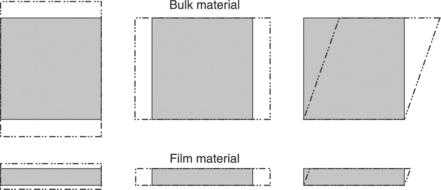
Now also consider the fact that a film, due to the limitations in mechanical strength, will not exist in isolation – it will be attached to a substrate, which will itself have an effect on the way in which the film responds to stimuli. In many cases there may be more than one other material system present. For instance, electrically activated systems will require support materials as well as electrode materials to be combined with the active film. When a film is combined with another material (i.e. a substrate), two effects take place due to the constraining effects of the non-active material. Firstly, the substrate will restrict the ability of the film to deform in the directions parallel to the substrate surface and, because the thickness and width deformations are related through the Poisson’s ratio of the film, the movement in the direction perpendicular to the substrate surface will also be reduced. Secondly, the presence of the non-deforming substrate will induce a bending moment in the film/substrate structure causing it to deform out-of-plane. This bending concept is the basis of a great many film actuators and can be found in cantilever, bridge and diaphragm actuators. The precise optimum ratio of the film and substrate dimensions will depend strongly on the material properties of the film and substrate materials, as well as the type of actuator. As a rough guide, the support material should be between one and two times as thick as the active film. Much less substrate material, and some of the active film, will be on the opposite side of the neutral axis and actively oppose motion. Conversely, too much substrate material and the substrate will resist deformation of the beam.
These thickness and bending modes are the basis of a multitude of microscale actuator devices. Bending mode devices are represented by low-frequency (kHz–MHz) ultrasound, actuators based on cantilevers, bridges and diaphragms, and electrical transformers. Thickness mode devices are represented by high frequency (MHz) ultrasound and surface acoustic wave type devices. In both cases, the operation of these devices is greatly influenced by the microstructure of the films. The microstructure of the films is, in turn, influenced by the processing conditions which, in turn, are dictated by the limitations of the materials used within the actuator.
14.3 Actuation mechanisms
14.3.1 Piezoelectricity
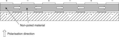
Piezoelectric materials are capable of exhibiting all three of the actuation mechanisms (longitudinal, transverse and shear) outlined at the start of this chapter. The parameters that describe these properties are related to the poling direction (direction 3) and the notation of the axis (British Standards Institution, 2002). For longitudinal and transverse actuation, the material is poled in the same direction as the applied electric field used to drive the actuator. For shear actuation, the poling direction is at 90° to the applied field. Longitudinal actuation is described by the parameter d33, which indicates that the applied field, represented by the first subscript, is applied in the direction of poling (3) and that the measured displacement, represented by the second subscript, is in the same direction (3), as depicted in Fig. 14.2. Transverse actuation is described by the parameter d31 which indicates the field is applied in the direction of poling (3) but the resultant displacement is at 90° to the applied field (1). Shear actuation in piezoelectric films is rare due to the difficulties of poling the film and applying electrodes at 90° to the poling direction. Shear is described by the parameter d15: the first subscript indicates that the applied field is at 90° to the poling direction (3), and the direction of motion, indicated by the second subscript, resulting from the relative shear motion of the two electroded surfaces is around the (2) direction. For piezoelectric ceramics, the three parameters shown are the only constants that are independent due to crystal symmetry. For further explanation of crystal symmetry, the authors recommend the book by Nye (1957).
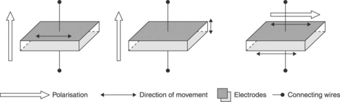
14.2 Schematic representation of transverse, longitudinal and shear actuation of piezoelectric materials.
Piezoelectric materials are an excellent choice for micro-sized actuators due to their excellent operating properties, which scale very well (Chang and Cohen, 1999), and the simplicity of design and use of the materials. One of the benefits of piezoelectric materials is that they generate high levels of force, making them ideal for actuation purposes. The disadvantage is that this high level of force is produced with a small strain, typically limited to 0.1%. In order to make use of this small strain to generate practical displacements, a mechanical amplifier needs to be used. The most straightforward mechanical amplifier is a simple cantilever but other innovative physical designs of actuator structure can also be used. At the heart of a mechanical amplifier is the principle that a high force/small strain can be converted to a low force/high strain. A classic bimetallic strip is a common example of this phenomenon, where the small differences in the thermal expansion of two different metals in intimate contact result in a significant strain as the strip bends. Individually, each material would exhibit microstrain but when placed in intimate contact along their length – constraining the touching faces to have the same length – the resultant beam will bend significantly when subjected to temperature changes. Any two materials connected in such a way will exhibit this effect, and it can be used to create printed film actuators that are controlled by changes in temperature.
In creating a piezoelectric bending mode actuator there are two design possibilities to stimulate such bending motion. The piezoelectric material can either be deposited onto an inactive material to create a unimorph structure (Fig. 14.3(a)) or two piezoelectric elements can be combined to create a bimorph structure (Fig. 14.3(b)). The unimorph structure is the most commonly utilised design in film actuators owing to the relative simplicity of fabrication (it is significantly easier to print a film on a substrate than it is to create a free-standing structure consisting of two printed films) and because the inactive material provides the necessary mechanical strength and toughness to prevent the device from failing. A bimorph can also be created by printing on both sides of an electrically conducting material that then acts as the central electrode, although this is not without difficulty in ensuring accurate registration of the two printed films.
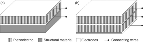
In the unimorph design the film is constrained by its connection to the passive layer. On actuation, the strain developed by the piezoelectric film is opposed by the passive material, resulting in the generation of internal stresses in the system, which causes the structure as a whole to bend. Common materials for the passive layer are silicon, thin film oxides such as SiO2 and SiNx, metals and ceramics such as alumina. Much work has been undertaken examining the first two groups due to the maturity of traditional silicon processing techniques used in the processing of micro electromechanical system (MEMS) devices (Madou, 2002). The alumina substrate cantilever is often favoured in screen-printing applications due to the ability to withstand higher processing temperatures and relative inertness of alumina with respect to other materials. A bimorph design can operate with no extraneous structural layers as it consists of two layers of the piezoelectric material sandwiched between conductive electrodes to define the structure. The layers can be operated in series or parallel (determined by the direction of poling in the constituent films and the connections to the electrodes). To generate a bending moment in such a structure, the layers that make up the device are operated in opposition to each other such that one layer expands while the other contracts. In the case of the serial-connected bimorph shown in Fig. 14.4(a), the poling directions within each of the films are in opposition when a voltage is applied across the structure as shown; one layer will expand while the other layer will contract, causing a bending displacement. If the poling in the films were in the same direction when a voltage was applied, a d31 expansion of both layers would be seen but no out-of-plane motion would be achieved. In a bimorph beam with a parallel connection, the poling direction of the constituent layers is the same, but the electric field is applied in opposite directions via a common connection to the two outer electrodes and a connection to the centre electrode (Fig. 14.4(b)). This ensures that the opposite strain effect is generated in each layer despite the poling directions being the same.
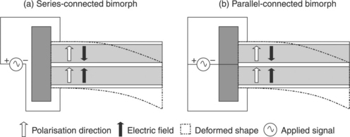
It should be noted that the terms ‘unimorph’ and ‘bimorph’ relate to the active material within the structure and not the overall structure. Both approaches consist of two main layers of material. However, it is common in the literature that the term ‘bimorph’ is used for both forms of device.
The cantilever, bridge and diaphragm type designs all make use of the lateral strain caused by the application of an electric field in the film thickness direction, e.g. d31 mode. Bridges and diaphragms are extensions of the cantilever concept with both ends fixed or the whole circumference fixed, respectively.
It is also possible to create such devices that make use of the d33 mode of actuation by employing interdigitated electrodes (IDE). In such devices, the piezoelectric film is still deposited as before, but the arrangement of the electrodes is markedly changed such that the applied electric field is in the lateral (in-plane) direction (Fig. 14.5). The rationale for this approach is that d33 is much larger than d31, so it should be possible to achieve a greater displacement. In practice, the performance of the two systems is comparable largely due to the inactive material under each electrode. For this reason, and the much simpler processing and better reliability, the d31 mode of actuation is still favoured.
The need to create small, reliable actuators is a driving force for development, pushing researchers to develop new piezoelectric materials and device designs, which exhibit greater strains and generate higher forces with shorter response times (Muralt, 2000). In conjunction with research on new materials for enhanced performance, another important aspect of research is environmentally friendly solutions for non-toxic piezoelectric materials, specifically lead-free ones. A key part of this work is addressing the issues associated with materials that contain volatile elements (e.g. Pb, Na, K). Such elements become volatised during processing, leading to depletion at the surface. For bulk materials, this is not generally a specific issue as the degraded material represents a small fraction of the total (or it can be removed easily), but for films, the presence of an inactive surface layer can significantly reduce the performance of the device as it represents a much larger fraction of the active material as a whole. For this reason there are often restrictions in the thermal processing temperature, which impacts the microstructure and performance (see section 14.6).
For film-based piezoelectric actuators, the most prolific materials are the ferroelectric perovskite ceramics such as lead zirconate titanate (PZT) and barium titanate (BaTiO3).
14.3.2 Magnetostriction
Magnetostrictive (MS) materials undergo a dimensional change through the application of a magnetic field. Such materials tend to be ferromagnetic in nature and it is the reorientation of anisotropic magnetic domains in the structure that gives rise to a macroscopic strain in a similar way to the ferroelectric domain reorientation giving rise to piezoelectric response.
Amorphous materials such as TbFe and SmFe alloys have high MS coefficients, but with low permeability require high external magnetic field to achieve significant actuation. Amorphous FeSiB and TbDyFe alloys exhibit higher permeability and thus enhanced responses. Exhibiting one of the highest MS behaviours, Terfinol-D is one of the most commonly employed MS materials and has a composition of around Tb0.3Dy0.7Fe1.9. Galfenol (Fe81.6Ga18.4) is MS material that exhibits greater ductility and machinablity with respect to Terfinol-D (Ueno et al., 2008) and is favoured when shaping of the MS material is required.
The advantage of MS actuators is that there is no requirement for complex electrical interconnects as the actuating (magnetic) field is applied externally. This means that a MS actuator can consist of just two materials – the MS material and the support material – making them extremely robust and reliable.
14.3.3 Shape memory alloy
Shape memory alloys (SMAs) form a group of metals that have the ability, when trained, to recover their shape under the application of heat due to a solid state phase transformation from martensite to austenite. At room temperature, the material has a highly twinned martensitic phase that can be easily plastically deformed through the action of stress. This easy deformation occurs due to the propagation of the twin boundaries, which gives rise to a macroscopic plastic deformation. On heating above the transition temperature, the material undergoes a phase change from the deformed twinned martensite phase to the austenitic phase. At a macroscopic level, this is seen as the material returning to its original trained shape. On cooling, the austenite phase retransforms to martensite, but in the highly twinned state, with no macroscopic dimensional changes. Up to 8% strain can be observed in these materials on strain recovery. In operation, the SME is first trained to a certain shape by annealing at elevated temperatures. The system is then deformed through the application of stress (e.g. springs or thermal expansion differences on cooling). On activation through the application of heat, the SMA will then attempt to return to its ‘trained’ shape, resulting in the actuation action.
In common with MS systems, SMAs do not require electrical drive circuits to be incorporated and can instead be actuated through a change in the ambient temperature. It is also possible to use resistive heating (either via current passage through the SMA itself or via separate heater elements located at strategic points in the device), which provides the ability to control temperatures locally and create faster response times as the volume of material being heated/cooled is much reduced. When the system cools, if the mechanical stress is still present (i.e. if there is a spring in the system), it will cause the actuator to return to the ‘stand-by’ state.
The most common of these SMA materials is the alloy of Ni-Ti with typical operating ranges of − 100 to + 100°C. The Cu-Ta alloy system also exhibits SMA behaviour and has a larger operating temperature range but shows a lower strain behaviour coupled with poor ageing characteristics where the martensite phase is stabilized over time and corrosion of the alloy occurs.
14.3.4 Viability of printing active materials
Piezoelectric materials can readily be formed into films using a variety of printing techniques combined with high temperature processing to bring about densification of the green body films. Unlike piezoelectric materials, the majority of MS and SMA materials are metallic in nature and do not lend themselves to printing-based processes, which typically require high processing temperatures in oxidative environments.
While MS- and SMA-based actuators can readily be fabricated using RF sputtering (Ishiyama and Yokota, 2008; Lee and Cho, 2008), it is more pertinent to this chapter to consider the cases where such actuators have been fabricated by screen printing or other powder-based printing methods. Thick-film MS actuators have been produced by screen printing where the active material (Terfinol-D) was mixed with a glass frit and an organic carrier (Grabham et al., 2002) to create a printable ink that was deposited onto alumina substrates and sintered at temperatures ranging from 400 to 890°C for between one and two hours. The sintering of SMA materials is much more challenging due to the rapid oxidation of Ti in the presence of oxygen (Zhang et al., 1992). Today the vast majority of SMA actuators employ SMA wire or sheet materials (Lan and Fan, 2010; Nespoli et al., 2010; Williams et al., 2010) instead of printed films.
For the printed MS actuators, the properties obtained were lower than that of pure Terfinol-D partially due to the presence of the glass frit but also due to residual porosity in the system. This dependence on microstructure is similar to piezoelectric systems (see section 14.6) where porosity and second phases reduce the performance of the active films.
Due to the processing limitations of the SMA and MS materials, the remainder of the chapter will focus on the application of piezoelectric materials for actuator applications.
14.4 Piezoelectric actuators
The most common structure for a piezoelectric film device is a simple rectangular beam, which has a plethora of practical uses. The cantilever uses the transverse d31 actuation mode where the expansion in-plane results in an out-of-plane motion due to the differential strain developed at the PZT–substrate interface.
Such devices have been used to align optical fibres where perfect alignment is essential to avoid unnecessary signal attenuation. The simple cantilever beam used Pb0.97Nd0.02(Zr0.55Ti0.45)O3 as the piezoelectric material integrated with a low temperature co-fired ceramic (LTCC) system (Tuominen et al., 2006). In use, an optical fibre was bonded to the surface of the cantilever and the cantilever was then actuated until the fibre was positioned to give maximum signal to the collection system. Similar structures have been achieved using screen-printed PZT on LTCC (Hrovat et al., 2006) for cantilever actuators. The composite sol-gel approach has also been used to deposit PZT on Si- (Dauchy and Dorey, 2007; Zhu et al., 2008), Ni- (Rocks et al., 2009) and Ni-based alloys (Inconel 750 – using a La 0.8Sr0.2MnO3 barrier) (Es-Souni et al., 2007) to create actuator structures operating using the bending and thickness modes.
Where the previous cantilever actuator made use of a single pair of electrodes to create an out-of-plane motion (i.e. up and down), a combination of multiple actuator areas on a single structure can give rise to far more complex motions. Combining two actuator circuits, along either side of an actuator beam, can enable a cantilever to be driven in-plane (i.e. side to side) with a simulated plate shear effect. The cantilever beam is effectively composed of two piezoelectric unimorph actuators each positioned along each edge of the beam, but connected along their entire length, as shown in Fig. 14.6. By operating these unimorph actuators out-of-phase to each other, one expands while the other contracts, generating an in-plane motion (Leighton et al., 2007). Unlike out-of-plane cantilevers, these in-plane actuators are symmetrical through their thickness (i.e. both top and bottom electrodes are identical and no substrate is present) so that no out-of-plane bending is generated.
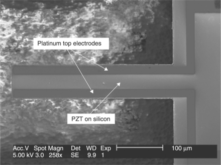
Combining multiple actuators together can create mechanical amplifier systems able to develop more complex motion paths. For example, multiple piezoelectric cantilevers can be combined within a single structure to generate motion such as the moving plate. This type of structure can be used as a scanning mirror for barcode readers or with the inclusion of a second conductive plate in close proximity a variable capacitor structure can be realised such as that demonstrated with four actuators by Park et al. (2001). Tani et al. (2007) have used piezoelectric beams incorporated into a silicon meander structure to create a complex scanning mirror that has X and Y scanning capability. When the films on adjacent beams are actuated in opposition to each other, a large deflection is generated; this translates in a static angle of 8.6°, which has applications in fibre optic switching, image display systems and adaptive lighting for vehicles. A still more complex structure consisting of three double-ended cantilevers has been used to create a microscale probe that is capable of describing motion in X, Y and Z directions (Claverley and Leach, 2010). Each actuator arm is composed of two independent actuators able to create more than just simple curvatures in the beam. Combining three of these actuators in a three-legged structure produces a device able to actuate in many different directions. Due to the small size of the features required for this device, a subtractive processing route was employed (Dorey et al., 2007), where the PZT was first printed and then the final shaping realised using wet etching.
14.5 Piezoelectric actuator fabrication
There are many ways to create film-based actuator structures using a printing approach. Broadly these can be classified as subtractive, where continuous films are printed and then material selectively removed to reveal the structure, and additive, where material is selectively deposited to create the structure directly (e.g. screen printing and ink-jet printing). Techniques such as screen printing have the advantage of only depositing the material that is required. The disadvantages are that less resolution and larger feature size are achievable (10s of μm) than with the subtractive techniques (Dorey et al., 2008). With subtractive techniques, once the desired functional film has been deposited, the next stage of processing is to remove the excess material that is not required for the functional device. This can be done chemically (e.g. acids), physically (e.g. powder blasting) or with the use of high-energy species (e.g. reactive ions) (Dorey, 2009). In all cases, it is first necessary to deposit a masking material that will protect the material that is to remain in place. The material is then exposed to the etching media until all of the unwanted material has been removed. Using this approach, much finer features (μm level) can be obtained.
Irrespective of which approach is adopted, the deposition and integration of the piezoelectric materials are at the heart of the process. In all cases, the key to the creation of thick-films is the reduction of the processing temperature so that the surrounding materials are not degraded. This can be achieved by using a low melting temperature sintering aid such as PbO (Yao et al., 2005), Pb5GeO11 (Duval et al., 2003), or Cu2O:4PbO (Dorey and Whatmore, 2002), which can reduce processing temperatures to between 700 and 950 °C allowing materials such as silicon, stainless steel, titanium and LTCC to be used instead of refractory materials such as alumina. The sintering aids enhance particle reorientation during the early stages of sintering and dissolution, atomic diffusion and repreciptitation during the latter sintering stages. While increasing density, they also introduce a second non-piezoelectric phase that can degrade functional properties, resulting in a need to balance the enhancing effect of increased density and the degrading effects of a second phase. Typically between 1 and 10 vol % of sintering aid is added to achieve optimum results. The exact level of sintering required will depend on the materials involved, the size of the particles in the ink and the processing temperatures used.
Alternatively, printed PZT ceramics can be infiltrated with a ceramic, producing sol (a metal organic precursor solution) to increase the density of the films (Lee, 2007). While the infiltration can be conducted after sintering, if it is done before sintering the maximum processing temperature can also be reduced (Dorey et al., 2003; Kwon et al., 2006). Higher numbers of infiltrations result in an increase in remnant polarisation, coercive field and relative permittivity. However, the piezoelectric coefficient can decrease due to increased clamping of the substrate and internal stresses (Dorey and Whatmore, 2002) caused by shrinkage of the sol during processing.
A logical extension of this approach is to create a printable ink composed of sol and powder (Kindl et al., 1991; Wu et al., 1993). By creating an ink where the conventional inert carrier fluid and binder are replaced by a ceramic producing sol, it is possible to produce a system where the sol serves the dual role of carrier fluid and binder. By compositionally matching the sol to the powder it is possible to produce high-density piezoelectric films at low temperatures with little presence of second phase.
14.6 Processing–properties–microstructure interrelationship
The desirable characteristics of an actuator include good reproducibility, low actuation drive requirements, fast response time, high strain and high force. Piezoelectric devices have an intrinsic fast response time. The strain and force response of the actuator will be a function of the piezoelectric coefficient, although it should be remembered that in general high strain/low force response is still obtained with cantilever devices, while low strain/high force response is obtained from thickness mode devices. High piezoelectric properties will simply enhance the response of a given type of actuator. Low actuation drive is reliant on high piezoelectric coefficients, as well as device designs that keep electrode separation as small as possible. This is best achieved where the film is actuated across its thickness or where small-spaced IDEs/multilayer electrodes are used. Reproducibility is maintained through a stable piezoelectric response. It can be seen that at the heart of all of these requirements is the need for a high and stable piezoelectric response.
While microstructural features affect the performance of all materials, the performance of thick-films is particularly sensitive to the microstructure of the film because it also affects the interaction with the substrate and the response of the device. In particular, the degree of actuation is affected not only by the piezoelectric properties of the material, but also by its elastic properties. For example, high piezoelectric properties coupled with low elastic properties may result in low degrees of actuation where the piezoelectric material is unable to deform the surrounding structure.
Examples of microstructural features (figure 14.7) that will affect the performance of thick-films include the following.
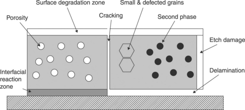
14.6.1 Second (inactive) phases
Such features are predominantly introduced in thick-films when sintering aids are used to enhance densification at low processing temperatures. They represent an inactive component that decreases the piezoelectric response of the film (Dorey et al., 2008). Interfacial reaction layers are another form of second phase that can arise when the piezoelectric materials react with the substrate, electrode or environment during processing.
14.6.2 Porosity
Pores mainly arise as a result of poor sintering caused by the need to use low processing temperatures. In an analogous way to second phases, the presence of porosity will decrease piezoelectric properties, but will also decrease the mechanical properties including stiffness and strength.
14.6.3 Defects and damage
Crystallographic defects may be present in thick-film materials due to the use of lower processing temperatures that do not allow the inherent defects in piezoelectric powders (caused by mechanical damage, limited crystallisation and residual unreacted phases) to be effectively annealed out. This will affect the ability of domains to move within the material and adversely affect the ability to pole the material and the piezoelectric properties. At the other extreme, processing damage (i.e. as a result of etching or cutting) will degrade a greater proportion of the material leading to more obvious degradation.
14.6.4 Grain size
The size of the grains is known to affect the piezoelectric properties of materials. With the use of lower sintering temperatures and reduced sintering, the size of grains in thick-films is often smaller than that found in bulk materials and below the optimum size for high piezoelectric properties to be obtained.
The main discrepancy between bulk and thick-film properties originates from the difference in microstructure caused by the need to use lower processing temperatures and constrained sintering when dealing with thick-films. As all the above microstructural features are affected by processing it is difficult to separate the effects. In general, thick-films have lower densities, more second phase, smaller grains and higher levels of internal defects, stress and constraint.
Where films exhibit a high density (< 5 vol% porosity), their elastic properties are approximately linearly dependant on porosity, but as the level of porosity increases the degradation in properties is much larger (Walter et al., 2002). The same behaviour is observed in d33 but not with trends in d31, where the piezoelectric properties are degraded significantly by relatively small levels of porosity. This has obvious implications for bending mode actuator devices that rely on high piezoelectric properties to achieve high deflection levels. Hence for bending mode devices the creation of high density films is of paramount importance. For some applications, such as resonant sensing devices, the magnitude of the piezoelectric coefficient does not affect the effectiveness of the device. Here, films with second phases and up to 30 vol% porosity achieved mass sensitivities as high as 30 pg/Hz (Park et al., 2006). The ability to use printed films to reduce the size of the resonating devices was the main reason for achieving such high sensitivities (Yi et al, 2003). Conversely, thickness mode actuation devices may be able to accommodate a certain degree of porosity, particularly if the substrate restraint is reduced by the presence of porosity as this can actually enhance the d33 response because the material is more able to deform in the thickness direction.
It is often observed that small-scale actuators do not perform as predicted by the models, which can give rise to a degree of disappointment. Such reduced performance can arise due to processing challenges in maintaining accurate dimensions and the effects of interfacial layers not included in models, as well as the reduced properties of the materials themselves.
As the size of the features decreases, the tolerances of the different manufacturing techniques begin to have a greater impact on the behaviour and reproducibility of the device as a whole. For example, a batch of 10 mm × 2 mm cantilevers produced with a tolerance of ± 10 μm would likely see a slight deviation from the predicted behaviour and a small variation in performance from one device to another. However, as the size of the device is reduced, the same variation in processing will have a much larger effect. So a batch of 1 mm × 0.2 mm cantilevers produced with the same tolerance of ± 10 μm would exhibit a significant variation across the batch and could also behave very differently from model predictions. This need to control the processing variance can often drive the choice of processing technology, with subtractive routes favoured for small devices and additive routes favoured for larger devices.
Another cause for deviation between model and device is the assumed properties of the materials. It is relatively straightforward to compensate for variances in mechanical properties caused by different microstructures (e.g. grain size, porosity, etc.) by adjusting the material data used in the models and redesigning the device based on updated figures. However, it becomes more complex to account for the variations in functional properties as these vary depending on the nature and relative size of the surrounding materials. This is particularly pertinent with piezoelectric materials as their piezoelectric properties are affected not only by the microstructure of the material but also by the chemical homogeneity and the surrounding stress states during processing and use.
As piezoelectric film actuators are generally used in a structure containing more than one layer, piezoelectric film behaves very differently from its bulk counterpart and this has a significant impact on the piezoelectric properties of the film. This change in behaviour results from the reduction in domain wall motion due to substrate clamping in the case of dij and the influence of substrate bending in the case of eij properties. Equations that compensate for these effects are shown below. Note that the dij and eij properties are denoted as film properties with the suffix f (Southin et al., 2001):
In general, all of the dij properties of piezoelectric thin films are reduced in comparison to their bulk counterparts with the same composition, while the eij properties of the piezoelectric thin films are in practice higher due to substrate bending-induced stresses in the film, which adds further charge contributions from deformation in other orientations. What is particularly challenging about using such predictions is that both the unconstrained mechanical and piezoelectric material properties depend on the microstructure of the material. In addition, these equations account for full clamping, but at an intermediate level of constraint deviations from these values will occur. These two points make it very difficult to predict accurately the behaviour of actuators from modelling alone. At this point it is worth noting that even comparing quoted material properties can be complicated by the fact that the properties quoted for films are often the film versions of the properties – i.e. d33, f.
Further compounding the issue is the assumption that the materials are fully poled. When printed films are produced they are invariably under a degree of tensile stress resulting from the shrinkage induced during processing. When films are poled through their thickness, this tensile stress opposes the poling field and can retard the degree of poling. This is seen clearly in measurements of ferroelectric hysteresis loops, which typically exhibit lower remnant polarisations and higher coercive fields, indicative of degraded domain reorientation (Dorey and Whatmore, 2002).
Finally, the very act of processing the materials during the manufacture of the device can lead to differences between the device’s performance and the model. Such discrepancies occur due to interfacial reactions that result in regions of material with different properties to that modelled. Size again is critical here, as the interfacial regions are likely to remain unchanged as the device is reduced in scale. So a 100 μm thick piezoelectric actuator with a 1 μm thick inactive interfacial or surface zone will not exhibit a significant variation from the predicted performance. Conversely, a 10 μm thick piezoelectric film with the same 1 μm inactive layer will exhibit at least a 10% reduction in performance. The interfacial layer remains approximately constant as it is controlled by the reaction kinetics, and for a given processing profile the reaction kinetics remain constant. Diffusion barrier layers can be used to prevent reactions between materials, but their very presence may in itself affect the performance of the device. This is seen in ultrasound devices where barrier layers above a certain size can start to interact with the acoustic waves. In cantilever devices, the incorporation of very thick, or highly stressed layers, can result in unexpected deformation of the device.
14.7 Conclusion and future trends
14.7.1 Polymer and composite active materials
While this chapter has focussed on the inorganic functional materials, there are a number of polymeric materials that also exhibit functional behaviour including piezoelectricity and SMA behaviour. With advances in plastic electronics and related printing technologies there is potential for this group of materials to be employed as actuators to a greater degree. Such materials can easily be printed using the same techniques used to print ceramic and metallic films but without the issues associated with controlling particle size, clogging and sintering. There are, however, other issues including lower properties and the need to mechanically treat polymeric films that need to be addressed before widespread uptake.
Individual carbon nanotubes (CNTs) are able to deform on the application of electrical signals and have been used as nano scale actuators (Li et al., 2008). While printed films of CNTs have not been used as the active material on their own in actuators, they have been used as part of actuators. Due to their conductive nature they can be applied as a monolayer and used as a transparent electrode, as shown by Yu et al. (2006), and even incorporated into electroactive polymers to enhance their performance. When embedded and aligned in a polymer matrix, CNTs have been shown to partially realign when an external electric field is applied. The resulting twisting motion of the CNTs within the polymeric matrix results in a macroscopic deformation of the composite. Printed films could feasibly be created using this approach.
14.7.2 Multiferroic active materials
Combining piezoelectric and magnetic behaviour, multiferroic (MF) materials offer increased flexibility with actuators that can be activated both electrically and magnetically. Historically, MF materials have exhibited relatively poor performance and MF activity has been achieved by combining ferromagnetic and piezoelectric materials to create a composite system. Recent developments in studies on BiFeO3 have shown that true MF materials with good properties exist and could be used in actuators. Dye-modified BFO (Bi0.7Dy0.3FeO3)-based cantilevers have been fabricated using pulsed laser deposition to create unimorph cantilever actuators 100–300 μm in length with Si as the substrate (Prashanthi et al., 2011). This shows great promise as MF materials can be handled and processed in the same way as ceramic piezoelectric materials for which there exists a great deal of processing knowhow.
14.7.3 Direct-write technologies
Along with advancements in new active materials and actuators designs, there is also significant interest in developing new and more flexible processing routes to directly print actuator materials. Where at one time screen printing and high-temperature firing were seen as the way to produce printed films (particularly with inorganic active materials), new technologies employing more flexible and precise fabrication capabilities are evolving. Of particular interest are techniques such as transfer printing, embossing/moulding (Wang et al., 2009), laser sintering and ink-jet (and related) droplet deposition techniques.
14.8 Further information and advice
Actuator design is constantly evolving and the role that printed films have to play in this evolution is growing. The vast majority of current commercially available actuator technologies are not based on printed film technology. In addition to the references in this chapter there are a number of generic texts on actuators and related devices including: review of non-film-based piezoelectric actuators by Watson et al. (2009) and review of microscale sensors and actuators by Wilson et al. (2007).
14.9 References
British Standards Institution. BS EN 50324-1:2002 Piezoelectric properties of ceramic materials and components. Part 1: Terms and definitions. Brussels: Cenelec, 2002; .
Chang, L., Cohen, Y.B. Scaling laws of microactuators and potential applications of electroactive polymers in MEMS. Proceedings of the SPIE’s 6th Annual International Symposium on Smart Structures and Materials. 1999. [SPIE, Newport Beach, California].
Claverley, J.D., Leach, K.L. A vibrating micro-scale CMM probe for measuring high aspect ratio structures. Microsystems Technology. 2010; 16:1507–1512.
Dauchy, F., Dorey, R.A. Thickness mode high frequency MEMS piezoelectric micro ultrasound transducers. J Electroceram. 2007; 19:383–386.
Dorey, R.A. Challenges in integration of piezoelectric ceramics in micro electromechanical systems. Materials Science Forum. 2009; 606:43–50.
Dorey, R.A., Whatmore, R.W. Apparent reduction in the value of the d33 piezoelectric coefficient in PZT thick-films. Integrated Ferroelectrics. 2002; 50:111–119.
Dorey, R.A., Whatmore, R.W., Beeby, S.P., Torah, R.N., White, N.M. Screen-printed PZT thick-films using composite film technology. Integrated Ferroelectrics. 2003; 54:651–658.
Dorey, R.A., Dauchy, F., Wang, D., Berriet, R. Fabrication and characterisation of annular thickness mode piezoelectric micro ultrasonic transducers. IEEE Transactions on Ultrasounics, Ferroelectrics, and Frequency Control. 2007; 54:2462–2468.
Dorey, R.A., Rocks, S.A., Dauchy, F., Wang, D., Bortolani, F., et al. Integrating functional ceramics into microsystems. Journal of the European Ceramic Society. 2008; 28:1397–1403.
Duval, F.F.C., Dorey, R.A., Zhang, Q., Whatmore, R.W. Lead germanium oxide sinter assisted PZT composite thick-film. Journal of the European Ceramic Society. 2003; 23:1935–1941.
Es-Souni, M., Maximov, S., Piorra, A., Krause, J., Solterbeck, C.-H. Hybrid powder-sol–gel PZT thick-films on metallic membranes for piezoelectric applications. Journal of the European Ceramic Society. 2007; 27:4139–4142.
Grabham, N.J., Beeby, S.P., White, N.M. The formulation and processing of a thick-films magnetostrictive material. Meas Sci Technol. 2002; 13:59–64.
Hrovat, M., Holc, J., Drnovsek, S., Belavic, D., Cilenšek, J., et al. PZT thick-films on LTCC substrates with an interposed alumina barrier layer. Journal of the European Ceramic Society. 2006; 26:897–900.
Ishiyama, K., Yokota, C. Cantilevered actuator using magnetostrictive thin film. Journal of Magnetism and Magnetic Materials. 2008; 320:2481–2484.
Kindl, B., Carlsson, D.J., Deslandes, Y., Hoddenbagh, J.M.A. Preparation of a-alumina ceramics: the use of boehmite sols as dispersing agents. Ceramics International. 1991; 17:347–350.
Kwon, T.Y., Park, J.H., Kim, Y.B., Yoon, D.S., Cheon, C.I., et al. Preparation of piezoelectric 0.1Pb(Zn0.5W0.5)O3-0.9Pb(Zr0.5Ti0.5)O3 solid solution and thick-films for low temperature firing on Si-substrate. J Cryst Growth. 2006; 295:172–178.
Lan, C.-C., Fan, C.-H. An accurate self-sensing method for the control of shape memory alloy actuation flexures. Sensors and Actuators A. 2010; 163:323–332.
Lee, S.-G. Effects of sol infiltration on the screen-printed lead zirconate titanate thick-films. Materials Letters. 2007; 61:1982–1985.
Lee, H.-S., Cho, C. Study on advanced multilayered magnetostrictive thin film coating techniques for MEMS applications. Journal of Materials Processing Technology. 2008; 201:678–682.
Leighton, G.J.T., Kirby, P.B., Fox, C.H.J. In-plane excitation of thin silicon cantilevers using piezoelectric thin films. Applied Physics Letters. 2007; 91:183510.
Li, C., Thostenson, E.T., Chou, T.-W. Sensors and actuators based on carbon nanotubes and their composites. Composites Science and Technology. 2008; 68:1227–1249.
Madou, M.J. Fundamentals of Microfabrication: The Science of Miniaturization, 2nd ed. Boca Raton: CRC Press; 2002.
Muralt, P. Ferroelectric thin films for micro-sensors and actuators: a review. Journal of Micromechanics and Microengineering. 2000; 10:136–146.
Nespoli, A., Besseghini, S., Pittaccio, S., Villa, E., Viscuso, S. The high potential of shape memory alloys in developing miniature mechanical devices: a review on shape memory alloy mini-actuators. Sensors and Actuators A. 2010; 158:149–160.
Nye, J.F. Physical Properties of Crystals: Their representation by Tensors and Matrixes. Oxford: Oxford University Press; 1957.
Park, J.Y., Yee, Y.J., Nam, H.J., Bu, J.U. Micromachined RF MEMS tuneable capacitors using piezoelectric actuators. International Microwave Symposium Digest. 2001; 3:2111–2114.
Park, J.H., Kwon, T.Y., Kim, H.J., Kim, S.R., Yoon, D.S., et al. Resonance properties and mass sensitivity of monolithic microcantilever sensors actuated by piezoelectric PZT thick-film. J Electroceram. 2006; 17:565–572.
Prashanthi, K., Mandal, M., Duttagupta, S.P., Pinto, R., Palkar, V.R. Fabrication and characterisation of a novel magnetoelectric multiferroic MEMS cantilever on Si. Sensors and Actuators A. 2011; 166:83–87.
Rocks, S.A., Tredez, Q., Almond, H.J., Shaw, C.P., Dorey, R.A. Bottom up fabrication of a nickel-lead zirconate titanate piezoelectric microcantilevers. Materials Letters. 2009; 63:88–90.
Southin, J.E.A., Wilson, S.A., Schmitt, D., Whatmore, R.W. e31, f determination for PZT films using a conventional ‘d33’ meter. Journal of physics D: Applied physics. 2001; 34:1456–1460.
Tani, M., Akamatsu, M., Yasuda, Y., Toshiyoshi, H. A two-axis piezoelectric tilting micromirror with a newly developed PZT-meandering actuator. 20th International Conference on Micro Electro Mechanical Systems. 2007:699–702. [Hyogo, Japan].
Tuominen, J., Lappalainen, J., Hiltunen, J., Ollilia, J., Lantto, V. Piezoelectric thin film unimorph actuator for optical fibre alignment applications. Journal of Optics A: Pure Applied Optics. 2006; 8:5398–5404.
Ueno, T., Summers, E., Wun-Fogle, M., Higuchi, T. Micro-magentostrictive vibrator using iron-gallium alloy. Sensors and Actuators A. 2008; 148:280–284.
Walter, V., Delobelle, P., Le Moal, P., Joseph, E., Collet, M. A piezo-mechanical characterization of PZT thick-films screen-printed on alumina substrate. Sensors and Actuators A. 2002; 96:157–166.
Wang, D., Rocks, S.A., Dorey, R.A. Micromoulding of PZT film structures using electrohydrodynamic atomization mould filling. Journal of the European Ceramic Society. 2009; 29:1147–1155.
Watson, B., Friend, J., Yeo, L. Piezoelectric ultrasonic micro/milli-scale actuators. Sensors and Actuators A. 2009; 152:219–233.
Williams, E.A., Shaw, G., Elahinia, M. Control of an automated shape memory alloy mirror actuator. Mechatronics. 2010; 20:527–534.
Wilson, S.A., Jourdain, P.J., Zhang, Q., Doregy, R.A., Bowen, C.R., et al. New materials for micro-scale sensors and actuators. An engineering review, Materials Science and Engineering R. 2007; 56:1–129.
Wu, J., Chen, M., Jones, F.R., James, P.F. Mullite and alumina–silica matrices for composites by modified sol-gel processing. J Non-Cryst Solids. 1993; 162:197–200.
Yao, K., He, X., Xu, Y., Chen, M. Screen-printed piezoelectric ceramic thick-films with sintering additives introduced through a liquid-phase approach. Sensors and Actuators A. 2005; 118:342–348.
Yi, J.W., Shih, W.Y., Mutharasan, R., Shih, W.-H. In situ cell detection using piezoelectric lead zirconate titanate–stainless steel cantilevers. J App Phys. 2003; 93:619–625.
Yu, X., Rajamani, R., Stelson, K.A., Cui, T. Carbon nanotube-based transparent thin film acoustic actuators and sensors. Sensors and Actuators A. 2006; 132:626–631.
Zhang, N., Khosrovabadi, P.B., Lindenhovius, J.H., Kolster, B.H. TiNi shape memory alloys prepared by normal sintering. Materials Science and Engineering. 1992; A150:263–270.
Zhu, B.P., Wu, D.W., Zhou, Q.F., Shi, J., Shung, K.K. Lead zirconate titanate thick-film with enhanced electrical properties for high frequency transducer applications. Applied Physics Letters. 2008; 93:012905.