
Printed resistive sensors for physical quantities
Abstract:
This chapter reviews commonly used and state-of-the-art versions of resistive sensors for physical quantities such as temperature, strain, radiant energy and magnetic field, relying on printed films. An outline is given for the properties of the films on which these sensors operate with a mention of their structure and applications.
7.1 Introduction
Academic and technical communities started to recognize the potential of thick-film technology in the field of solid state sensors about 40 years ago. Research and development efforts resulted in a notable impact of thick-films in measuring systems (Prudenziati, 1994; White and Turner, 1997). Nowadays, thick-film resistive sensors are well assessed especially in applications where high reliability and long-term stability in very demanding environments are requisites to be complied with economically, such as in large market sectors like automotive applications (Wada et al., 1997), or in uncommon operations (e.g. appropriate performance in large facilities) or disposable devices. The innovations achieved in the 1980s with traditional thick-film materials and processes were extended during the next two decades with low-temperature co-fixed ceramics (LTCC) technology for Micro Electro-Mechanical Systems based on structured Ceramic materials (C-MEM) and micro-machined Micro Electro-Mechanical Systems based on micro-machined Silicon (Si-MEMS). Recently, some researchers have been exploring the new frontiers of fine-line printing technologies, such as ink-jet printing for mesoscale sensor systems. This chapter reviews commonly used and state-of-the-art versions of resistive sensors for physical quantities, i.e. temperature, strain, radiant and magnetic field-related quantities. Also applications of potentiometric thick-films will be briefly mentioned. An outline is given for the properties on which these sensors operate with a mention of their structure and applications. Thick-film physical sensors relying on capacitive devices and pyro–piezo electric thick-films materials are covered in chapters 8 and 9 respectively; thick-film chemical sensors are dealt with in chapters 10 and 11; biosensors are in chapter 13. Finally physical sensors relying on non-resistive thick-films forming parts of MEMS are described in chapter 10 of this book. The references quoted here are merely a sample of the huge quantities of studies published on resistive printed sensors and their applications.
7.2 Temperature sensors
Thick-film materials can be used for temperature measurements. A major advantage of this technique is its capability to integrate the temperature sensing function with the sensor signal conditioning circuitry. These thick-film sensors, when formed on ceramic or insulated metal substrates, can withstand much greater abuse and handling than the normal metallic wire thermocouples. This class of sensors includes: resistive temperature detectors (RTD), positive temperature coefficient sensors (also denoted as PTC thermistors), negative temperature-coefficient (NTC) thermistors, thick-film thermocouples, thermo-switches, cryogenic and low temperature detectors.
7.2.1 Resistive temperature detectors
Thick-film conductors, either simple metals or alloys (typical sheet resistance from 1.5 to 200 mΩ/![]() ) exhibit thermoresistive properties similar to those of their bulk counterparts, that is to say that their electrical transport is governed mainly by electrons scattered from lattice defects and vibrations. The latter phenomenon (also denoted as phonon scattering) is the most influential at temperatures not too far from room temperature, resulting in a quasi-linear temperature dependence of resistivity and consequently of the resistance. The R(T) vs. T relation over a temperature span of many hundreds of degrees is in fact:
) exhibit thermoresistive properties similar to those of their bulk counterparts, that is to say that their electrical transport is governed mainly by electrons scattered from lattice defects and vibrations. The latter phenomenon (also denoted as phonon scattering) is the most influential at temperatures not too far from room temperature, resulting in a quasi-linear temperature dependence of resistivity and consequently of the resistance. The R(T) vs. T relation over a temperature span of many hundreds of degrees is in fact:
where T is temperature in degrees Centigrade and R0 denotes resistance at a reference T, e.g. 0 °C. Alternatively, the simpler linear equation,
may be used to represent the sensor response, typically in a range from − 55 to 125 °C.
The temperature coefficient of resistance (TCR) = α assumes values as high as 7000 ppm/°C in pure Ni and 3850 ppm/°C in pure Pt. These two metals are in fact the basic elements of the well-known wire-wound and thin-film RTD sensors.
Thick-film versions of RTDs were introduced starting with various conductive thick-film inks (Arima, 1994). The addition of glass or oxide binders (required to promote sintering and adhesion, as discussed in Chapter 4) is responsible for an added contribution to the electron scattering, or, in practice, to an increase of resistivity and decrease of TCR values. Hence, it is not surprising that these performance characteristics are affected by the preparation conditions, including the firing temperature and dwell time: all of the conditions promoting increased densification and grain growth of metal particles result in performance approaching that of the parent metal. Similarly, larger TCR values are displayed by fritless thick-film RDT than their glass-bonded counterparts. Therefore reproducibility of results requires close control of paste composition and preparing process.
Although Ni and several precious metal-based inks are of interest in manufacturing RTDs, it is Pt that plays a dominant role in thick-film RTD thermometry. A multipurpose RTD Pt-based sensor has been manufactured by Matthew Electronics since 1975, and commercially available under the trademark Thermafilm®, with a 100 Ω resistance at 0 °C and a TCR of 3850 ppm/°C. It meets the BS 1904 and DIN 43 760 standards, providing direct replacement for conventional wire-wound temperature detectors, with operating temperatures up to 600 °C and excellent stability (e.g. temperature error < 1 °C at 600 °C/6000 h; Evans, 1981). In addition, in thick-film sensing systems for other physical, chemical and biological quantities, screen-printed temperature sensors are essentially omnipresent, and often Pt-based elements are chosen not only for their high-temperature sensitivity but also for their stability in a variety of harsh environments without degradation.
A common drawback of metal-based thick-film conductors is the relatively low sheet resistance of the fired layers. Thus high aspect–ratio configurations are required for yielding easily measurable resistance of the elements. A partial remedy is the use of metal–organic-based pastes, resulting in thinner (0.1–0.3 μm) fired films with higher sheet resistance (e.g. 1 to 3 Ω/![]() ) than conventional thick-film materials, without sacrifice of TCR (e.g. Pt-based Heraeus RP 10003). For these films the substrate has to be glazed or very smooth, and several multiple layers are deposited and separately fired. RTDs of about 3 × 9 mm with a resistance of 100 Ω have been obtained in this way (Reynolds and Norton, 1986). Another route to increase the sensor resistance is to pattern fine (10–20 μm wide) lines, a procedure early executed with YAG-laser trimming of the deposited films; now micropen deposition or ink-jet printing processes are promising methods, that are currently under scrutiny (Cai et al., 2009). However, the most common way to cope with the main requirements of high sensitivity, small size and easily measurable resistance in temperature detectors is the use of cermet thick-film materials referred to as thermistors.
) than conventional thick-film materials, without sacrifice of TCR (e.g. Pt-based Heraeus RP 10003). For these films the substrate has to be glazed or very smooth, and several multiple layers are deposited and separately fired. RTDs of about 3 × 9 mm with a resistance of 100 Ω have been obtained in this way (Reynolds and Norton, 1986). Another route to increase the sensor resistance is to pattern fine (10–20 μm wide) lines, a procedure early executed with YAG-laser trimming of the deposited films; now micropen deposition or ink-jet printing processes are promising methods, that are currently under scrutiny (Cai et al., 2009). However, the most common way to cope with the main requirements of high sensitivity, small size and easily measurable resistance in temperature detectors is the use of cermet thick-film materials referred to as thermistors.
7.2.2 Positive temperature coefficient thermistors
Thick-film compositions for PTC thermistors with sheet resistances from 10 to 1000 Ω/![]() have been developed (e.g. PTC 2100 or 2600 by ESL and 5090 by DuPont). The linear R(T) vs. T relation in eq. [7.2] is representative of the sensor response with TCR values spanning from 2500 ppm/°C to 4500 ppm/°C. A possible way to prepare PTC sensors is to start from resistive inks comprising an adequate glass frit and a fine powder of complex perovskite oxides such as CaCu3Ru4O12 and/or LaCu3Ru4O12 (Burkhardt et al., 1993) resulting in thermistors with sheet resistances from about 50 to 500 Ω/
have been developed (e.g. PTC 2100 or 2600 by ESL and 5090 by DuPont). The linear R(T) vs. T relation in eq. [7.2] is representative of the sensor response with TCR values spanning from 2500 ppm/°C to 4500 ppm/°C. A possible way to prepare PTC sensors is to start from resistive inks comprising an adequate glass frit and a fine powder of complex perovskite oxides such as CaCu3Ru4O12 and/or LaCu3Ru4O12 (Burkhardt et al., 1993) resulting in thermistors with sheet resistances from about 50 to 500 Ω/![]() and TCR from 1000 to 2000 ppm/°C in the temperature range − 25 to + 125 °C. Another way is to ‘load’ the glass phase with a large fraction of RuO2. The relatively low specific resistivity of RuO2 and its metallic-like temperature dependence R (T) with a TCR of a few 1000 ppm/°C allows designers to create PTC sensors with α values typically in the range from 1000 to 1500 ppm/°C with sheet resistance around 1–10 Ω/
and TCR from 1000 to 2000 ppm/°C in the temperature range − 25 to + 125 °C. Another way is to ‘load’ the glass phase with a large fraction of RuO2. The relatively low specific resistivity of RuO2 and its metallic-like temperature dependence R (T) with a TCR of a few 1000 ppm/°C allows designers to create PTC sensors with α values typically in the range from 1000 to 1500 ppm/°C with sheet resistance around 1–10 Ω/![]() (see Chapter 4, section 4.1, for sheet resistance definition). Likewise, Kuzel et al. (1993) successfully prepared cermets compositions based on Bi2Ru2O7, CdO and two types of glass for sensors with sheet resistance of 0.5–3 kΩ/
(see Chapter 4, section 4.1, for sheet resistance definition). Likewise, Kuzel et al. (1993) successfully prepared cermets compositions based on Bi2Ru2O7, CdO and two types of glass for sensors with sheet resistance of 0.5–3 kΩ/![]() and TCR of 2200–2600 ppm/°C.
and TCR of 2200–2600 ppm/°C.
A very special composition (and microstructure) for PTC sensors is represented by the resistive series DuPont 5090D with sheet resistance ranging from 10 to 1 KΩ/![]() and TCR of about 3500 ppm/°C. The member 5091D, 10 Ω/
and TCR of about 3500 ppm/°C. The member 5091D, 10 Ω/![]() , is claimed to exhibit a Pt-like behaviour e.g. to match exactly the α and β coefficients of the linear and quadratic terms in the R(T) vs. T response (eq. [7.1]) of platinum standard sensors. These sensors are due to Cu2O added to ruthenate-based pyrochlores in high-lead glass promoting the dissociation of the ruthenate compound, e.g. Pb2Ru2O6,5 (Hormadaly, 1990; Jiang et al., 2000) or (Gd,Bi)2Ru2O7 (Hrovat et al., 2007), which partially transforms during firing in needle-like RuO2 grains (Fig. 7.1).
, is claimed to exhibit a Pt-like behaviour e.g. to match exactly the α and β coefficients of the linear and quadratic terms in the R(T) vs. T response (eq. [7.1]) of platinum standard sensors. These sensors are due to Cu2O added to ruthenate-based pyrochlores in high-lead glass promoting the dissociation of the ruthenate compound, e.g. Pb2Ru2O6,5 (Hormadaly, 1990; Jiang et al., 2000) or (Gd,Bi)2Ru2O7 (Hrovat et al., 2007), which partially transforms during firing in needle-like RuO2 grains (Fig. 7.1).
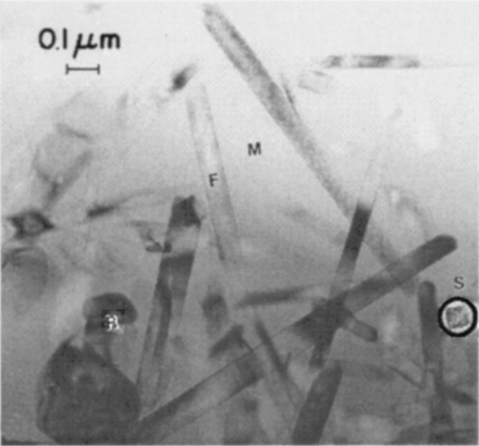
7.1 The ruthenate conductive phase in thick-film resistors decomposes due to interactions with a glass phase into RuO2. Due to added copper oxide, the RuO2 crystallizes in the form of needle-like grains. Bright field Transmission Electron Microscopy (TEM) micrograph of 5093 thermistor: RuO2 elongated particles are denoted F, RuO2 equiaxed particles are denoted R, M is a matrix region and a cross-section is circled at S (after Jiang et al., 2000).
7.2.3 Negative temperature coefficient thermistors
NTC thermistors’ compositions e.g. ESL-NTC 2100 (http://www.electroscience.com/pdf/NTC-2100.pdf), Ferro-4900 (http://www.ferro.com/non-cms/EMS/EPM/HIC//HIGH-VOLTAGE/4900-thermistors.pdf), and e.g. the former DuPont NTC40 and NTC50, complement the chances offered to designers of thick-film circuits and systems with NTC components.
Thick-film NTC compositions differ from those of NTC-thermistors manufactured in ceramic technology at least in one of the following features: (1) glass is added to the functional material to promote adhesion at the substrate/ film interface, (2) a metal-like powder is added to control the sheet resistance, (3) the form of the functional material: it may be present in the ink either as a powder of the final oxide or as precursors that react during the thermal annealing to form the sensitive oxide, (4) lower peak temperature and dwell time for the sintering process. However, in both types of NTC thermistors (thick-films and ceramic), the functional material is a solid solution of transition metal oxides, such as Mn3O4, Co3O4, NiO, with the spinel structure (general formula AB2O4; Arima, 1994). It is generally accepted that their conductivity is due to a thermally activated phonon-assisted hopping of charge carriers between cations of differing oxidation state on the octahedral sites of the spinel structure (Park and Bang, 2003). The specific resistance ρ vs. temperature is described by the Arrhenius equation:
where ρ0 is the resistivity (Ω cm) at ‘infinite’ temperature, T is the absolute temperature and B = Ea/kB is the thermistor constant (also called the beta factor or the coefficient of temperature sensitivity), Ea is the activation energy for electrical conduction and kB is the Boltzmann constant.
The values of the resistivity and the beta factors of NTC materials depend not only on the composition (ratio between the main oxides, minor addition of other oxides, e.g. Cu2O, Fe2O3), but also on the sintering temperature and annealing treatments. The resistivity of the spinel compounds at room temperature ranges from a few hundreds of Ω cm to a few tens of KΩ cm, the beta factor from 2500 to 4000 K and the temperature coefficients of expansion from 8.5 × 10− 6/°C to 14.3 × 10− 6/°C (Arima, 1994).
Since screen-printed and fired films are usually 10 to 20 μm thick, the numerical value of the sheet resistance Rs (Ω/![]() ) of the film turns out to be two and three orders of magnitude higher than the resistivity (Ω cm) of the material (according to the ‘rule’: Rs = ρ/t, where t is the thickness: see section 4.2.1, Chapter 4), resulting in resistances too high for practical applications. In order to overcome this shortcoming, enhanced by the presence of the glass phase, a further phase with a low specific resistance is added to the ink. The latter is often RuO2. In appropriate amounts, this also serves to decrease the current noise and improve the stability of the sensors. However, due to the high positive TCR of RuO2, it also decreases the beta factor.
) of the film turns out to be two and three orders of magnitude higher than the resistivity (Ω cm) of the material (according to the ‘rule’: Rs = ρ/t, where t is the thickness: see section 4.2.1, Chapter 4), resulting in resistances too high for practical applications. In order to overcome this shortcoming, enhanced by the presence of the glass phase, a further phase with a low specific resistance is added to the ink. The latter is often RuO2. In appropriate amounts, this also serves to decrease the current noise and improve the stability of the sensors. However, due to the high positive TCR of RuO2, it also decreases the beta factor.
Like the majority of thick-film resistors, PTC and NTC thick-film thermistors were developed for firing on relatively inert alumina substrates. The compatibility of existing pastes with LTCC systems is far from being straightforward. Because of shrinkage, mismatch and difference in thermal expansion coefficients, the tapes may cause the thermistors to deform during the firing process and vice versa. Moreover, physicochemical interactions between the paste and the tape may affect the thermistor characteristics. Investigations carried out on films prepared with the same paste and fired on 96%-Al2O3 and on (or between adjacent) LTCC tapes either co-fired or post-fired (Hrovat et al., 2005, 2009; Zhong and Bau, 2001) not surprisingly showed different microstructures and electrical properties (sheet resistance, calibration curves, noise), but only in a few circumstances were the changes found to be detrimental for the use of the sensor/LTCC multilayer. Adverse results, such as delaminations, were observed with thermistors buried inside the LTCC structure forming cavities between adjacent LTCC tapes, when a significant mismatch in sintering rate of the thermistor and LTCC was allowed (Hrovat et al., 2009). With accurate matching of thermistors–tape composition and process parameters (preferably Ag-free terminations, optimum firing cycle and deposition on top of the LTCC structure), close tolerance in resistance and TCR (e.g. < 10% and 2%, respectively) were achieved (Birol et al., 2004). Otherwise, for precise temperature readings, individual calibrations are required.
Direct laser trimming of thick-film thermistors on their support adds to thick-film thermistors the potential benefit of devices with tightly matched reference resistance; however, great care has to be taken in setting the proper trimming parameters in order to limit the inevitable heating, resulting in a lack of control of the target resistance value (A. M. Stein, private communication).
Thick-film thermistors are incorporated in the design of a variety of hybrid circuits and sensors for thermal compensation. Thick-film RTDs are almost omnipresent with printed thick-film gas sensors (either as an integrated component to measure and assist the control of the operation temperature, or with the simultaneous functions of heater and temperature detector). In several microfluidic devices that monitor flow-rate, and in minute chemical and biological reactors, thermistors play a critical role (Jurków and Golonka, 2009). In addition, RTDs are present in humidity sensors (Nicolics and Smetana, 1991), water quality control, in inclinometers (Birol, 2007), microwave circuit control (Feingold et al., 1998) and flow sensors (Wada et al., 1997; Bartsch de Torres et al., 2010), (Fig. 7.2), etc.
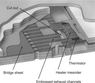
7.2 Sensor design of a thick-film flow sensor for biological microsystems, with thermistor compositions printed on a free-standing bridge and encapsulated to ensure biological compatibility (after Bartsch de Torres et al., 2010).
7.2.4 Thermocouples
Thermocouples and thermopiles operate on the thermoelectric (Seebeck) effect: an electromotive force (e.m.f.:voltage) appears when two different conductors are joined and the junctions are exposed to different temperatures. The e.m.f. is proportional to the temperature difference ∆T, via a Seebeck coefficient σab. Therefore, thermocouples and thermopiles are not ‘resistive’ sensors, strictly speaking; also, they are not widely used as temperature-sensing elements but in other interesting applications such as in planar, cheap infrared thermal detectors, laser power detectors (Smetana and Reicher, 1997), thermoelectric generators (Markowski and Dziedzic, 2008; Ohta et al., 1990; Weber et al., 2006) and thermoelectric coolers. Also, the measurement of the Seebeck voltage (sometimes in conjunction with the resistive response) has been found to be effective in improving the selectivity of chemoresistive printed gas sensors (e.g. Ionescu, 1998).
Relative Seebeck coefficients (σab) for couples of selected commercial conductive pastes are in the range of 5 to 20 μV/K, whereas σab up to 450 μV/K for (Sb2Te3)72(Bi2Te3)25(Sb2Te3)3–(Bi2Te3)95(Sb2Se3)5 have been reported (Ohta et al., 1990).
7.2.5 Low-temperature, cryogenic sensors
Thick-film cermet resistors made from RuO2 or bismuth ruthenate pastes, introduced as cryogenic sensors in the early 1980s, are today typically referred to as ruthenium oxide (chip) RTDs (Postma, 1994; Rubin, 1991). These RTDs are essentially the same, in composition and manufacturing processes, as the TFRs exhibiting a near-zero TCR at 300 K. Yet, their resistance starts to increase sharply below liquid nitrogen temperature, making them useful low-temperature sensors. Moreover, their outstanding low magneto-resistance and the possibility of predicting the low-temperature R(T) characteristic from the room temperature resistance (Willekers et al., 1990), render them a strong competitor to other known RTDs, especially from 40 K down to 10 mK. In fact, these devices have the lowest magneto-resistance below 1 K of any commercially available RTD (Affronte et al., 1998; Watanabe et al., 2001; Yeager and Courts, 2001). These characteristics, in addition to good immunity to ionizing radiation, recently found thick-film RTDs’ application in the critical temperature control of the superconducting magnets in CERN’s Large Hadron Collider (Ylöstalo et al., 1996). They were also used as cryogenic sensors in the ARCADE experiment investigating the cosmic microwave background radiation (Fixsen et al., 2002; Kogut et al., 2004).
Suppliers of commercial thick-film RuO2-chips (e.g. Oxford Instruments, UK and Scientific Instruments, USA) resort to special mounting strategies to accomplish optimum thermal contact, stability, wiring and measurement accuracy. Integrated small calorimeters for measurements at cryogenic temperatures have been also designed and tested (Mach et al., 2003).
7.3 Piezoresistive properties and related sensors
Sensors of strain-related mechanical quantities relying on the piezoresistive properties of thick-film resistors (TFRs) are actually one of the most successful areas of application for printed sensors. Strain, load, force, acceleration and pressure are measured with thick-film piezoresistors, mainly based on ruthenium dioxide (RuO2) or ruthenates as conductive phases. Resistance changes in TFRs were first noticed in the early 1970s, as described by Holmes, but the effect was considered to be more of a hindrance because of the induced stresses when circuits were potted in resins (Holmes, 1973). Holmes makes no mention of the potential of using the effect as a sensing mechanism in the form of a strain gauge. A few years later, the first studies of piezoresistive effects emerged while researchers were trying to collect a comprehensive picture of the physical properties in TFRs, which could fit in a suitable electrical transport model for this type of cermet resistor (Canali et al., 1980; Morten et al., 1977; Pike and Seager, 1977). The decisive step in exploitation of the effects may be recognized in the patent filed by F. I. Marelli in 1979, followed soon by the industrial production of pressure sensors for automotive applications (Cattaneo et al., 1980). Since then, piezoresistive properties of TFRs have attracted a great deal of scientific and technological interest and applications have rapidly spread in many diversified areas (Morten and Prudenziati, 1994). According to concepts, materials and methods of the current thick-film technology, devices were first prepared on alumina substrates; it is interesting to note that the term ‘ceramic sensors’ was coined for these devices to recognize the contribution given by alumina to the sensors’ performance due to its corrosion resistance in aggressive media, refractory nature and low cost.
Figure 7.3 is a schematic of a typical pressure sensor based on a ceramic diaphragm and body (base plate). Thick-film conductors, resistors and sealing glasses are printed and fired to make the sensor. The four piezoresistors form a bridge on the diaphragm. Applying pressure deflects the diaphragm, thus resulting in an imbalance in the bridge network and in a corresponding proportional output signal. With minor modifications in the size (4–15 mm diameter) and thickness (0.25–1.3 mm) of the diaphragm, it is possible to cover a pressure range from about 0.1 to 50 MPa with an accuracy better than 1–2% (Dell’Acqua and Dell’Orto, 1986). This type of design can be used to produce all three types of pressure sensors: absolute, differential and relative. A variety of other substrates were considered in further designs, including other ceramic materials such as zirconia (Chitale et al., 1992), enamelled steel (Prudenziati et al., 1981/1982), insulated steel (Brignell et al., 1988, Marioli et al., 1993; White 1989), aluminium and titanium (Jacq et al., 2004a, 2004b) and LTCC (Hrovat et al., 2003, 2006).
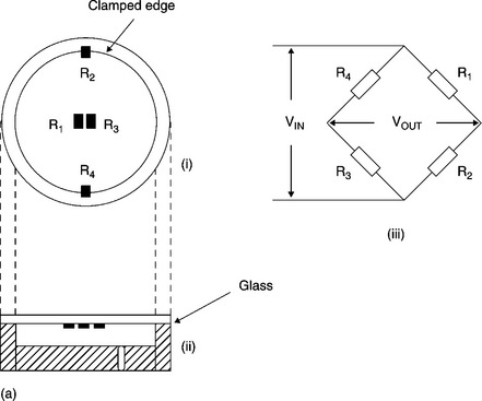
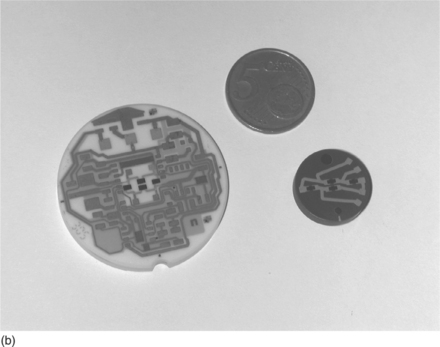
7.3 (a) Schematic drawing of a thick-film ceramic pressure sensor. (i) sensing resistors on the diaphragm; (ii) set up of the diaphragm on the body; (iii) Wheatstone bridge configuration. (b) Two realized designs: on the left, a sensor based on ceramic diaphragm and body; on the right, insulated steel membrane on steel body. (courtesy of Hybritec International, Italy),(courtesy of Gefran, Italy)
Alumina is superior to all of these substrates in terms of dielectric strength, corrosion resistance and the matching of the thermal expansion coefficient with that of the largely available TFRs. However, alumina is surpassed by other substrates in terms of flexural strength and elastic modulus (Table 7.1).
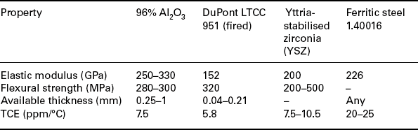
In addition, insulated metals and LTCC are very easily machined, formed and processed in a workshop. Particularly interesting in this picture are LTCC tapes for their low elastic modulus, which is about three times lower than that of standard alumina substrates, and their otherwise comparable elastic and electrical properties. One example of applications taking advantage of these properties is represented by the successful implementation of millinewton load sensors down to 100 mN full scale (Birol et al., 2007).
City Sensor, France; WIKA, Germany; Impress Sensors & Systems, England; DJ Instruments, USA; Metallux Electronic, Switzerland; Hybritec International, Italy; Baumer, USA; Gefran, Italy; and Hipot, Slovenia, are among the companies that manufacture commercial devices based on thick-film piezo-resistors. I could not confirm whether Fiat Italy is still active in manufacturing this type of sensor for applications for their own internal use.
Features that render thick-film piezo-resistors attractive from a technical as well as a speculative point of view, encompass:
• Strain responses ∆R/R vs. ε (where ∆R/R is the relative change of resistance due to the applied strain ε) linear, symmetrical (for tensile and compressive strains), hysteresis-free (at least up to about 1000 με, i.e. the breaking point of alumina substrates and near the upper limit of elastic behaviour of insulated metal substrates), with the following features:
• Gauge factors (GF ≡ ∆R/R ε) in the range from 2 to 35, according to the composition of the paste, firing cycle, terminations, substrate; hence a gauge factor intermediate between those of metal and semiconductor strain gauge, accompanied by:
• The low temperature coefficient of resistance (TCR ≡ ∆R/R∆T) and of gauge factor (TCGF ≡ ∆GF/GF∆T, of a few hundreds ppm/°C);
• Negligible changes of resistance under (even very intense) magnetic fields, light intensity, electric fields, nuclear radiation;
• A good stability up to comparatively high temperatures (125–150 °C);
• Large immunity to severe conditions, thermal shock, vibrations, acceleration.
Investigations aimed at identifying the best materials and processes have been performed on either commercial pastes or model systems. The picture emerging from studies on RuO2-based and ruthenate-based resistors shows the following properties.
The measured longitudinal gauge factor GFl (strain ε parallel to the current I) and transverse gauge factor GFt (ε perpendicular to I) are both positive (i.e. R increases in tensile stress) with GFl > GFt, being frequently GFl − GFt ~ 2 (1 + ν), where ν is the Poisson’s ratio of the substrate, just as expected, under simplifying assumptions, for isotropic materials (Fawcett and Hill, 1999).
TFRs of the same series (i.e. based on the same conductive phase and the same or similar dielectric matrix) exhibit increasing strain sensitivity (GF values) at decreasing conductive volume fraction, i.e. at increasing sheet resistance Rs (Canali et al., 1980; Tamborin et al., 1997).
TFRs having the same Rs but coarser conductive particles exhibit larger GF values shown in Figure 7.4 (Tamborin et al., 1997).
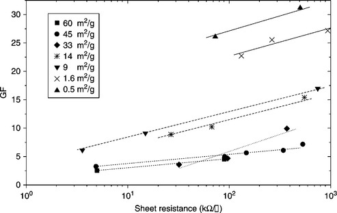
7.4 Strain sensitivity of RuO2-based TFRs prepared with powders of various sizes, as a function of the sample sheet resistance.
Model resistors prepared with Bi2Ru2O7, RuO2, CaIrO3, IrO2 powders of similar size were compared (Prudenziati et al., 1997); the strain sensitivity appeared to be unaffected by the nature of the conductive oxides except for samples fired at high temperatures (e.g. 850–950 °C) where the compositions of the glassy matrix changed as a result of interactions with the conducting phase. The role of the glass composition remains unclear. It was suggested that addition of oxides (e.g. BaTiO3, MoO3) and metal (e.g. Mo, K, Fe) provide ‘super GF factors’, i.e. GF values larger than 30, up to 200–300 (Abe and Takeda, 1986). Unfortunately these modifiers are responsible for asymmetric responses under compressive and tensile stresses, lack of linearity in ∆R vs. ε response, very high noise levels and crack lines running on the resistor’s surface. Moreover, it was shown that the artificial (false) ‘super-gauge factors’ are to be ascribed to defects (cracks and fissures) in the glassy matrix: when these defects are ‘healed’ (closing them with glues) the asymmetric response disappears and ‘normal’ GF values are recovered (Prudenziati et al., 1989).
Correlations between compositions, sheet resistance, gauge factors, TCR and excess noise have been studied in model systems prepared with the same glass frit and RuO2 powders covering a range of particle sizes from a few nanometers to micrometers (Tamborin et al., 1997), resulting in samples with sheet resistance Rs in the range from 200 Ω/![]() to 3 MΩ/
to 3 MΩ/![]() . At a selected Rs value, the GFl increases linearly with the logarithm of RuO2 grain size, while the TCR and excess noise do not significantly depend on the RuO2 powder size. Similar investigations by researchers in Dresden (Dietrich et al., 2009) opted for the conductive/glass size–particle ratio as the parameter for RuO2-based resistors with the same sheet resistance (10 KΩ/
. At a selected Rs value, the GFl increases linearly with the logarithm of RuO2 grain size, while the TCR and excess noise do not significantly depend on the RuO2 powder size. Similar investigations by researchers in Dresden (Dietrich et al., 2009) opted for the conductive/glass size–particle ratio as the parameter for RuO2-based resistors with the same sheet resistance (10 KΩ/![]() ). In addition, the ageing stability was also measured. The increase of GF values by increasing the RuO2 particle size was confirmed, whereas the results on TCR and noise index were in substantial disagreement (probably because of the different composition of the glassy phase, although in both studies it was a lead–silicate glass).
). In addition, the ageing stability was also measured. The increase of GF values by increasing the RuO2 particle size was confirmed, whereas the results on TCR and noise index were in substantial disagreement (probably because of the different composition of the glassy phase, although in both studies it was a lead–silicate glass).
In all TFRs, either prepared with commercial pastes (bearing ruthenates, RuO2 a mixture of these compounds) or model systems, the best compromise between the strain sensitivity and noise spectral density, hence the optimum signal-to-noise ratio of piezoresistors, can be achieved with resistors of intermediate sheet resistances, e.g. Rs in the 10 KΩ/![]() (Hrovat et al., 2001).
(Hrovat et al., 2001).
Considerably less copious is the harvest of data available on piezo effects in TFRs based on a conductive phase other than a Ru-compound. Ir O2-based resistors with lead–silicate glass offer similar behaviour in terms of sensitivity and TCR, with the additional benefit of higher stability up to 175 °C but also higher cost (Tankiewicz et al., 2002).
Sensitivity to stress applied normally to the printed piezoresistor is about twice that experienced with uniaxially applied stress, in accordance with the resolved components of the stress and the low stiffness of the film as compared with its substrate (Fawcett and Hill, 1999; Puers et al., 1987). Thick-film piezoresistors under hydrostatic pressure invariably exhibit ∆R/R∆p of the order of 20–30 (Fawcett and Hill, 1999). Also notable is the persistence of the high gauge factors down to liquid helium temperatures (Ferrero et al., 1990).
No systematic study has been performed with lead-free thick-film piezoresistors. However, in some explorative investigations, no interesting strain sensitivity was experienced so far in either RuO2-based (Morten et al., 1991) or CaRuO3-based systems (Rane et al., 2007).
A deeper knowledge of the resistors’ microstructure and advanced computational methods for modelling these complex phenomena are paving the way for a satisfactory interpretation of the physical origin of the mentioned effects. A separate contribution in this volume (Grimaldi, Chapter 5) describes the approaches used and the actual level of understanding of the mechanisms of electrical transport and mechanical–electrical phenomena occurring in cermet TFRs. In brief, the results show that the coexistence of electron tunnelling and percolation phenomena, together with the heterogeneity of the microstructure, are responsible for the strain sensitivity of the resistors. Their segregated structure is responsible for the non-marked difference in GFl and GFt, whereas a gauge factor (GF) enhancement results from the highly heterogeneous dispersion of conducting phases, which are stiffer than the insulating one. Therefore, the local strains within the matrix are enhanced with respect to the averaged macroscopic strain.
Polymer-based TFRs, such as carbon resistors, offering the chance of thermal cure at low temperatures (typically 125–150 °C) and consequently the possibility of printing on flexible organic substrates, were promising for sensors envisaged for low pressure and/or low load sensors. However, no suitable materials were identified. The resistors were generally characterized by lack of linearity, significant hysteresis, high TCR and low sensitivity. Pseudo-plastic effects of the substrates (e.g. Mylar) and the matrix of the carbon-conducting phase were signalled as responsible for this deluding performance (Arshak et al., 1995).
7.4 Magnetoresistive effects and sensors
Contactless sensors relying on magnetoresistive properties of screen-printed and fired films based on either metal ferromagnetic materials and perovskite oxides have been realized. Properties of the materials and films, choice of structure and sensor type are briefly delineated here.
In ferromagnetism, close relationships exist between electrical transport and magnetization, resulting in the dependence of the resistivity on the direction of the magnetization vector: measurements of the resistivity with the current I parallel (ρ//) or perpendicular (ρ⊥) to the magnetization direction provide different figures, with ρ// > ρ⊥ in most cases, as a consequence of the anisotropic scattering of the conduction electrons. The quantity:
where ρo = (ρ// + ρ⊥)/2, is defined as anisotropic magneto-resistance (AMR) and assumes typical values of a few percentage points. In the more general case of the current flowing at a θ angle with respect to M, the expression of ρ reads as:
This property is the basis of a variety of many thin film sensors. In thin films, vapour deposited or sputtered, the saturation magnetization direction is ‘entailed’ by an external magnetic field applied parallel to the plane of the substrate during the deposition process or in the next annealing, and ‘constricted’ on the film plane because of the large demagnetizing field normal to the film plane. The most common composition for these films is Ni81Fe19, which does not exhibit magnetostrictive effects, exhibits a relative high Curie temperature of 850 °C, and, according to a general rule for alloys, a TCR much lower than that of the parent elements (Bozorth, 1993; Dibbern, 1986).
A search for magneto-resistive properties of ferromagnetic-metal based screen-printed films was performed first in films prepared with commercial air-fireable Ni-based pastes, developed for non-sensing applications (e.g. cathodes in gas discharge displays). In these pastes, the strong tendency of Ni to get consistently oxidized at high firing temperatures is contrasted by a ‘passivation effect’ provided by boride glassy and crystalline phases, e.g. AlB10, Ni3(BO3)2 and/or boron–lead silicate glassy phases (Sirotti et al., 1990). The complex microstructure of the films, with Ni accounting for only 70 to 80%wt in the fired layer, and limited growth of Ni grains even after treatments up to 900 °C, result in: (1) resistivity and TCR values not too dissimilar to those of Ni-bulk, (2) poor AMR ratio (Morten et al., 1990).
Nevertheless, special designs, aimed at achieving a reasonable degree of immunity to thermo-resistive effects, allowed designers to realize prototypes of interesting contactless sensors for linear position, speed of rotation and linear distance measurements (Morten et al., 1997).
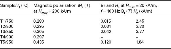
Improved properties were looked for with the development of nitrogen-fireable pastes based on NiCo alloys. Two approaches where followed: either in situ alloy formation (and sintering) from fine powders (1–5 μm) of Ni and Co in the ratio Ni:Co = 4:1 (samples referred to as Ni/Co-based films) or the sintering of a Ni80Co20 powder (1–1.5 μm particles) obtained by co-reduction of Ni(II) and Co(II) acetates with a polyol process (samples referred to as Ni80Co20; Bianco et al., 2000; Gusmano et al., 1996). The pastes, with no other constituents but the organic vehicle, were printed and fired in N2, on alumina substrates previously glazed with a calcium–silicate glass layer fired in air at 1000 °C to achieve adequate adhesion. Films prepared at increasing firing temperatures (750 °C–1000 °C) exhibit increasing magnetic polarization Ms (Masoero et al., 1999) and a decrease of the coercive field Hc, which are interpreted as natural consequences of perfected sintering and alloy formation in Co-Ni phase in one type of films and sintering of Ni80Co20 fine powders in the other films (Table 7.2).
Table 7.2
Magnetic properties of NiCo-based thick-films prepared at various peak firing temperatures Tf, Ms and remanent magnetization Br, in Tesla, coercive field Hc in kA/m
The microstructure exhibited carbonaceous residues due to incomplete burning of the organic vehicle, as well as porosities and oxidized regions due to residual oxygen partial pressure in the firing furnaces; these contribute to making the films magnetically harder than a corresponding bulk alloy. The temperature dependence of the saturation magnetization is very weak until at least 200 °C and follows the Curie–Weiss behaviour with a Curie temperature of 697 °C. Compared with Ni-based magneto-resistors, the new ferroelectric thick-film compositions exhibit a notably improved AMR value (Fig. 7.5 and Table 7.3) due to the enhanced longitudinal response added to the very low (essentially negligible) transverse response. Also a sensitivity S of the longitudinal response for H > Hsat is of interest for application purposes. However, the major actual drawback of these systems is due to the remarkable deterioration of the magneto-response at increasing ambient temperature. For example, the maximum ∆R/Rlong at Hsat in Ni80Co20 films fired at 950 °C follows the trend shown in Table 7.4.
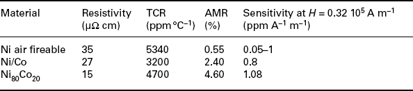
Table 7.4
Temperature dependence of the maximum ∆R/R (at Hsat) measured in the longitudinal response of Ni80Co20-based TF–MRs

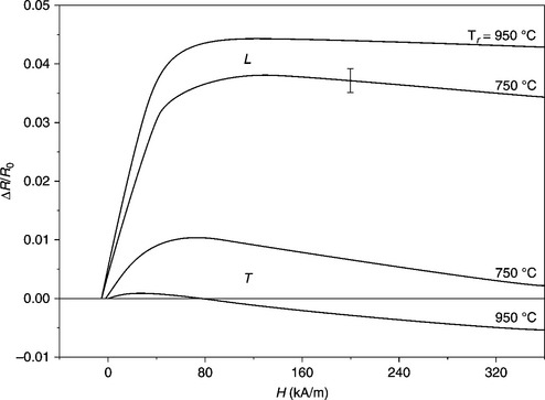
7.5 Comparison of the longitudinal (L) and transverse (T) magnetoresistance of two layers of Ni/Co = 70/30 alloy prepared with different peak firing temperatures (Tf) and measured at room temperature, as a function of Þeld H. R0 is the resistance measured in zero field.
The ferromagnetic properties of the films do not justify this result (according to the Ms vs. T behaviour) but the high TCR values of the Thick-Film-Magnetoresistors (TF-MRs) do (Table 7.3): the large increase in R0 makes the ∆R/R0 progressively lower at increasing T values.
Nowadays the same drawback afflicts the second family of printed magneto-resistors described in the literature, i.e. ferromagnetic screen-printed perovskites. This class of materials, chiefly manganites (notably La-A-Mn-O with A = Ca, Ba, Sr manganites), is a subject of very active research since the discovery of their anomalous high magneto-resistance close to the Curie temperature Tc. In addition, this effect is enhanced and extended to a wider temperature range in polycrystalline materials (Fig. 7.6).
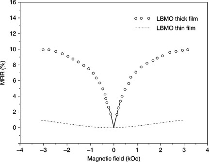
7.6 Variation of magneto-resistance ratio (MRR) for screen-printed and epitaxial thin film of La0.67Ba0.33MnO3 (LBMO) with magnetic field. The field is varied from zero to 3 kOe (240 A/m) and back to zero. (adapted from Khare et al. 2004)
Magneto-resistance ratio MRR (defined as MRR = (ρH − ρ0)/ρ0, where ρ0 and ρH are the resistivity measured at zero and H fields, respectively) as large as 90% have been observed at low temperatures (Viret et al., 1997) and the application of relatively low magnetic fields promotes a substantial reduction of the resistivity (low-field MRR, LFMR). This effect can be enhanced by using submicroscopic particles and LFMR values of about 30% can be routinely obtained, e.g. at low temperature in the range of field of 104 A/m. It has been found that the magneto-transport behaviour in manganites can be attributed to a double exchange mechanism between pairs of Mn3 + and Mn4 + ions. In this mechanism, a parallel alignment of the manganese spins is required before the electron can transfer between the ions to give charge transport. Application of an external magnetic field enhances the spin ordering and thus suppresses the resistivity. With a decrease of temperature there is a natural increase in alignment of spins, the resistivity decreases and the MRR vanishes, as observed in epitaxial films. On the other hand, in polycrystalline samples, such as screen-printed films, there is an additional source of MRR due to grain boundaries. A sharp increase in MRR at low field is attributed to spin-polarized tunnelling across the boundaries. The boundaries provide a kind of thin insulating barrier for electron tunnelling together with a magnetic decoupling of grains. Application of a small magnetic field aligns the randomly oriented grains and thus increases the tunnelling with the consequent decline in resistivity. Furthermore, the magnetic field applied at low temperatures (T < Tc) reduces the spin-dependent grain-boundary scattering of charge carriers (Khare et al., 2004).
This substantial LFMR has been used to design magneto-resistive magnetic thick-film sensors, e.g. a magnetic position sensor (Balcells et al., 1996), a magnetic potentiometer (Balcells et al., 2000), an angular position sensor, an on–off switch (Rubi et al., 2006). However, applications at or above room temperature are dampened by the fact that the LFMR decays rather fast with temperature and becomes almost negligible (< 0.05%) already below the Curie temperature (Tc < 360 K in La1 − xAxMnO3). The proposed alternative was to use the LFMR exhibited by the Sr2FeMoO6 oxides (Tc > 410 K). The synthesis of these materials resulted in a variety of subtle problematic issues related to stoichiometry, purity and disorder (Fe/Mo antisites), which was progressively overcome (Fontcuberta et al., 2002). The second alternative to overcome the issue of decay in LFMR(T) of manganese perovskites was recognized in the presence of the anisotropic magneto-resistance (AMR), which offers a relative resistance change of about 0.25% and 0.1% at 300 K and 350 K respectively, for a magnetic field H = 100 Oe (about 6 × 10³ A/m) parallel to the film plane (Balcells et al., 2002). The prospects for further progress in both materials preparation and opportunities for new oxides with still higher Curie temperatures are discussed in Foncuberta et al. (2002).
7.5 Radiant sensors
Already in 1995 researchers in RCA Laboratories at Princeton, USA (Nicoll and Kazan, 1955; Thomsen and Bube, 1955) were applying thick-film technology just as a cost-effective production process for solid state sensors. In fact, R. H. Bube (Thomsen and Bube 1955) describes highly sensitive photoconductive layers prepared, ‘by a “paint” of cadmium sulfide or selenide (a water mixture of sulfide or selenide with chloride and copper) onto a suitable surface, and firing the surface with its dried layer to form a polycrystalline sintered layer’. Thick-film photoconductors based on CdS, CdSe and CdInSe have been intensively studied in the past 45 years. The main changes in electrical and optical characteristics resulting from oxygen chemisorptions, residual Cu and Cl ions, sintering atmosphere and firing cycles have been understood and a lot of knowledge accrued in studies performed in several research centres, e.g. in India (Amalnerkar et al., 1980); Germany (Battelle Institute), Belgium (Ghent State University), Japan (Matsushita and Toshiba), UK (Southampton University), to cite a few. A review of thick-film CdS-based sensors has been provided by Setty and Amalnerkar (1994) and new applications of CdS-CdSe-based thick-films described by Ross (Ross 1995). In addition, the search for cheap production techniques for solar energy conversion devices has triggered the development of printed photovoltaic cells. This field also has been addressed in many countries, with the most intense activities in the decade between 1980 and 1990. Thick-film CdS/CdTe heterojunctions appear to be the most promising candidate and a conversion efficiency of around 10% has been demonstrated (Ikegami and Uda, 1994; Uda et al., 1997).
Photoconductive cells have seen a long, prosperous life on the market. Hamamatsu Photonics has manufactured and supplied CdS photo-cells for decades, until it recently (2006) ceased this production as a direct result of the Restriction of Hazardous Substances in Electrical and Electronic Equipment (RoHS) Directive, which restricts the import of Cd-containing products to the European Union (http://hamamatsu.com). The commercial production of screen-printed and sintered CdS/CdTe solar cells by Matsushita Battery Industrial Company started in January 1986 (Ikegami and Uda, 1994) and modules for different applications appear in the Panasonic Solar Cell Handbook (August 1998; see http://downloads.solarbotics.com/PDF/sunceramcat.pdf) under the tradename SunCeram II. We cannot confirm that production is continuing in this case.
7.6 Potentiometric sensors
As the name indicates, the potentiometric sensor consists in a variable resistance and wiper device. The primary design elements of such a system are a resistor and a wiping contact enclosed in a suitable package. The voltage drop across a potentiometer or variable resistor is monitored to achieve the desired control. The ratiometric output signal is proportional to the angular or linear position of the wiping contact (wiper). Both, linear and non-linear types of output signals can be obtained by appropriate design of the variable resistor. Applications of such systems include fluid level gauges (Fig. 7.7) and flow meters, while in addition, in automotive applications they are found in brake wear life gauges and position sensors to monitor valves and suspension and/or steering components. Automotive subsystems utilizing this type of sensor include electronic fuel injection, active suspension and exhaust gas recirculation (Wada et al., 1997).
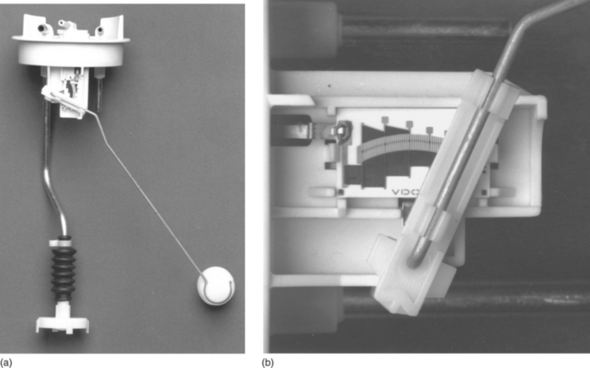
7.7 A fluid level sensor: the wiper of a thick-film potentiometer is connected to a lever arm (a). Any change in fluid level causes a change in the float lever arm assembly (b) thus providing an output signal proportional to the position of the wiper on the resistor track.
Depending on the application, the thick-film material can be of cermet or polymer composition. Typical wiping contacts are metallic and are designed to complement the device performance. The high reliability greatly overshadows the relatively low accuracy (0.5–2%) of devices based on thick-film materials. The thick-film materials offer the required fine line definition, accurate trimming, linearity, low noise, high abrasion and corrosion resistance for these types of devices.
7.7 Conclusion and future trends
The driving force of development in resistive thick-film physical sensors has been the need for cheap, reliable, stable devices and systems for harsh environments. As shown in this chapter and in the vast literature on the subject, a variety of successful products and applications has been accomplished. Future markets can be envisaged however, in which other demands, such as a reduction in size, integration with printed electronics and very large-scale mass production, will be the priorities. Therefore efforts might be at a premium in the evaluating printing methods such as MicroPen® and ink-jet printing, with the related issue of ink composition. Likely studies of interactions between both cermets and polymer-based inks and new, mostly flexible, substrates have to be addressed. These approaches should also be promising for the introduction of thick-film physical sensors into new market sectors such as in biomedical instrumentation and diagnostic devices and in portable electronic devices. Of course, a deeper and clearer understanding of electrical transport in cermet resistors and research into the electrical properties of complex oxides would support the advanced performance of devices already present in the actual panorama of thick-film physical sensors.
7.8 References
Abe, O., Takeda, Y. Strain characteristics of thick-film resistors and its application to a strain sensor. IMC 1986 Proceedings, Kobe, Japan, May. 1986:282–284.
Affronte, M., Campani, M., Morten, B., Prudenziati, M., Laborde, O. Magnetoresistance of RuO2-based thick-film resistors. Journal of Low Temperature Physics. 1998; 112:355–371.
Amalnerkar, D.P., Setty, M.S., Pavaskar, N.R., Sinha, A.P.B. Studies on thick-films of photoconducting cadmium sulphide. Bulletin of Material Science. 1980; 2(4):251–264.
Arima, H. Thick-film thermistors and RTDs. In: Handbook of Sensors and Actuators, 1 (Thick-film Sensors). UK: Elsevier; 1994:127–150.
Arshak, K.I., Ray, A.K., Hogarth, D.G., Collins, C.A., Ansari, F. An analysis of polymeric thick-film resistors as pressure sensors. Sensors and Actuators. 1995; A49(1–2):41–45.
Balcells, L., Calvo, E., Fontcuberta, J. Room-temperature anisotropic magnetoresistive sensor based on manganese perovskite thick-films. Journal of Magnetism and Magnetic Materials. 2002; 242–245:1166–1168.
Balcells, L., Enrich, R., Mora, J., Calleja, A., Fontcuberta, J., et al. Manganese perovskites: thick-film based position sensors fabrication. Applied Physics Letters. 1996; 69(10):1486–1488.
Balcells, L., Carrillo, A.E., Martinez, B., Sandiumenge, F., Fontcuberta, J. Room temperature magnetoresistive sensor based on thick-films manganese perovskite. Journal of Magnetism and Magnetic Materials. 2000; 221:224–230.
Bartsch de Torres, H., Rensch, C., Fischer, M., Schober, A., Hoffmann, M., et al. Thick-film flow sensor for biological microsystems. Sensors and Actuators A. 2010; 160(1–2):109–115.
Bianco, A., Gusmano, G., Montesperelli, G., Morten, B., Prudenziati, M., et al. Microstructure and surface composition of ferromagnetic thick-films prepared with NiCo Polyol derived powders. Thin Solid Film. 2000; 359:21–27.
Birol, H.Doctoral thesis, Fabrication of low temperature co-fired ceramic (LTCC)-based sensor and micro-fluidic structures. École Polytechnique Federale De Lausanne, 2007.
Birol, H., Maeder, T., Jacq, C., Ryser, P. Effects of firing conditions on thick-film ptc thermistor characteristics in LTCC Technology. IMAPS Conference on Ceramic Interconnect Technology. 2004:106–109.
Birol, H., Maeder, T., Nadzeyka, I., Boers, M., Ryser, P. Fabrication of a millinewton force sensor using low temperature co-fired ceramic (LTCC) technology. Sensors and Actuators, A: Physical. 2007; A134(2):334–338.
Bozorth, R.M.Ferromagnetism. New York: IEEE, 1993.
Brignell, J.E., White, N.M., Cranny, A.W.J. Sensor applications of thick-film technology. IEE Proceedings. 1988; 135:77–84.
US Patent No. 5 244 601 (14 September 1993)
Cai, Z., Li, X., Hu, Q., Zeng, X. Laser sintering of thick-film PTC thermistor paste deposited by micro-pen direct-write technology. Microelectronic Engineering. 2009; 86:10–15.
Canali, C., Malavasi, D., Morten, B., Prudenziati, M., Taroni, A. Piezoresistive effects in thick-film resistors. Journal of Applied Physics. 1980; 51:3282–3288.
Cattaneo, A., Dell’Acqua, R., Dell’Orto, G., Pirozzi, L., Canali, C. A practical utilization of the piezoresistive effect in thick-film resistors: a low cost pressure sensor. Proceedings of the International Microelectronics Symposium. 1980:221–228.
Chitale, S.M., Huang, C.Y.D., Stein, S.J., Wada, T. Piezoresistivity in high thick-film resistors: sensor design and very thin YSZ substrates. Proceedings of 7th International Microelectron Conference, Yokohama, Japan. 1992:561–570.
Dell’Acqua, R., Dell’Orto, G. High pressure thick-film monolithic sensors, 1986. [SAE Paper 860474, Detroit].
Dibbern, U. Magnetic field sensors using the magnetoresistive effect. Sensors and Actuators. 1986; 10(1–2):127–140.
Dietrich, S., Kretzschmar, C., Partsch, U., Rebenklau, L. Reliability and effective signal-to-noise ratio of RuO2-based thick-film strain gauges: the effect of conductive and glass particle size. 32nd International Spring Seminar on Electronics Technology, ISSE 2009. 2009:1–6.
Evans, W.D.J. Thick-film platinum resistance temperature detectors. The development and manufacture of advanced types for industrial and domestic applications. Platinum Metals Review. 1981; 25:2–11.
Fawcett, N., Hill, M. The electrical response of thick-film resistors to hydrostatic pressure and uniaxial stress between 77 and 535 K. Sensors and Actuators A. 1999; 78(2–3):114–119.
Feingold, A., Wahlers, R.L., Amstutz, P., Huang, C., Stein, S.J., et al. New microwave applications for thick-film thermistors. Proc SPIE, Vol. 3582, Proceedings of the 1998 International Symposium on Microelectronics. Technical Program Committee and IMAPS Staff, 1988.:179–184. [assembled and edited by the 1998].
Ferrero, C., Marinari, C., Masoero, A., Morten, B., Prudenziati, M. Performance of thick-film strain gauges at cryogenic temperatures. Cryogenics. 1990; 30:726–729.
Fixsen, D.J., Mirel, P.G.A., Kogut, A., Seiffert, M. A low noise thermometer readout for ruthenium oxide resistors. Review of Scientific Instruments. 2002; 73(10):3659–3663.
Fontcuberta, J., Balcells, L., Bibes, M., Navarro, J., Frontera, C., et al. Magnetoresistive oxides: new developments and applications. Journal of Magnetism and Magnetic Materials. 2002; 242–245:98–104.
Gusmano, G., Bianco, A., Montesperelli, G., Morten, B., De Cicco, G., et al. Preparation and properties of new thick-film magnetoresistive materials. Sensors and Actuators A. 1996; 52:161–165.
Holmes, P.J. Changes in thick-film resistor values due to substrate flexure. Microelectronics Reliability. 1973; 12:395–396.
Thermistor composition, US Patent 4 961 999 (9 October 1990)
Hrovat, M., Belavič, D., Samardzija, Z., Holc, J. A characterization of thick-film resistors for strain gauge applications. Journal of Materials Science. 2001; 36:2679.
Hrovat, M., Belavič, D., Bencan, A., Bernard, J., Hole, J., et al. Thick-film resistors on various substrates as sensing elements for strain gauge applications. Sensors and Actuators A. 2003; 107:261–272.
Hrovat, M., Belavič, D., Kita, J., Cilenšek, J., Golonka, L., et al. Thick-film temperature sensors on alumina and LTCC substrates. Journal of the European Ceramic Society. 2005; 25:3443–3450.
Hrovat, M., Belavič, D., Kita, J., Holc, J., Drnovšek, S., et al. Thick-film strain and temperature sensors on LTCC substrates. Microelectronics International. 2006; 23(3):33–41.
Hrovat, M., Belavič, D., Kita, J., Holc, J., Cilenšek, J., et al. Thick-film PTC thermistors and LTCC structures: the dependence of the electrical and microstructural characteristics on the firing temperature. Journal of the European Ceramic Society. 2007; 27:2237–2243.
Hrovat, M., Belavič, D., Kita, J., Holc, J., Cilenšek, J., Drnovšek, S., Thick-film NTC thermistors and LTCC materials: the dependence of the electrical and microstructural characteristics on the firing temperature. Journal of the European Ceramic Society 2009; 29:3265–3271. http://sales.hamamatsu.com/en/products/solid-state-division/compound-semiconductors/cds.php
Ikegami, S., Uda, H. Screen-printed CdS/CdTe solar cells. In: Prudenziati M., ed. Thick-Film Sensors. Amsterdam: Elsevier, 1994.
Ionescu, R. Combined Seebeck and resistive SnO2 gas sensors, a new selective device. Sensors and Actuators B. 1998; 48:392–394.
Jacq, C., Maeder, T., Ryser, P. High-strain response of piezoresistive thick-film resistors on titanium alloy substrates. Journal of the European Ceramic Society. 2004; 24(6):1897–1900.
Jacq, C., Vionnet, S., Maeder, T., Ryser, P. Integrated thick-film hybrid microelectronics on aluminium substrates. Proceedings of the European Microelectronics and Packaging Symposium, Prague. 2004.
Jiang, J.C., Crosbie, G.M., Tian, W., Cameron, K.K., Pan, X.Q. Transmission electron microscopy structure and platinum-like temperature coefficient of resistance in a ruthenate-based thick-film resistor with copper oxide. J Appl Phys. 2000; 88(2):1124–1128.
Jurków, D., Golonka, L. Novel cold chemical lamination bonding technique, a simple TCC thermistor-based flow sensor. Journal of the European Ceramic Society. 2009; 29(10):1971–1976.
Khare, N., Moharil, U.P., Singh, B., Gupta, A.K. Study of low field magneto-resistance in La0.67A0.33MnO3 (A ≡ Ca, Ba, Sr) screen-printed films. Indian Journal of Pure and Applied Physics. 2004; 42(1):62–66.
Kogut, A., Wollack, E., Fixsen, D.J., Limon, M., Mirel, P., et al. Design and calibration of a cryogenic blackbody calibrator at centimeter wavelengths. Review of Scientific Instruments. 2004; 75:5079–5083.
Kuzel, R., Koprivova, E., Broukal, J. Thick-film resistors with high TCR. Microelectronics International. 1993; 4(1):28–31.
Mach, M., Pietriková, A., Gabàni, S., Pavlìk, V., Flachbad, K., et al. Low temperature micro-calorimeters based on thick-film resistors. 26th International Spring Seminar on Electronics Technology, Stará Lesná, Slovak Republic. 2003.
Marioli, D., Rolla, P., Taroni, A. Insulated metal substrates for thick-film sensors applications. Proceedings of 9th European Hybrid Microelectronics Conference (Nice). 1993:261–268.
Markowski, P., Dziedzic, A. Planar and three-dimensional thick-film thermoelectric microgenerators. Microelectronics Reliability. 2008; 48:890–896.
Masoero, A., Morten, B., Olcese, G.L., Prudenziati, M., Tango, F., et al. Magnetic properties of Ni-Co thick-film magnetoresistors. Thin Solid Films. 1999; 350:214–218.
Morten, B., Prudenziati, M. Piezoresistive thick-film sensors. In: Prudenziati M., ed. Thick-film Sensors. Amsterdam: Elsevier; 1994:189–208.
Morten, B., Prudenziati, M., Taroni, A., Piezoresistenza in resistori a film spesso depositati per serigrafa. Digest AEI Conference. 1977. [(unpublished)].
Morten, B., Prudenziati, M., Sirotti, F., DeCicco, G., Alberigi-Quaranta, A., et al. Magnetoresistive properties of Ni-based thick-films. Journal of Materials Science: Materials in Electronics. 1990; 1:118–122.
Morten, B., Ruffi, G., Sirotti, F., Tombesi, A., Moro, L., et al. Lead-free ruthenium-based thick-film resistors: a study of model-systems. Journal of Materials Science: Materials in Electronics. 1991; 2(1):46–53.
Morten, B., Prudenziati, M., De Cicco, G., Bianco, A., Montesperelli, G., et al. Thick-film magnetoresistors and related sensors. Measurment Science and Technology. 1997; 8:21–28.
Nicolics, J., Smetana, W. A laser power detector built up by application of thick-film technology. Sensors and Actuators A. 1991; 25–27:235–239.
Nicoll, F.H., Kazan, B. Large area high-current photoconductive cell using cadmium sulphide powder. Journal of the Optical Society of America. 1955; 45:647–650.
Ohta, T., Kajikawa, T., Kumashiro, Y. Characteristics of (Bi, Sb)2(Te, Se)3-based thick-film thermoelectric elements for power generation. Electrical Engineering in Japan. 1990; 110:14–23.
Park, K., Bang, D.Y. Electrical properties of Ni–Mn–Co–(Fe) oxide thick-film NTC thermistors prepared by screen printing. Journal of Materials Science: Materials in Electronics. 2003; 14(2):81–88.
Pike, G.E., Seager, G.H. Electrical properties and conduction mechanisms of Ru-based thickfilm (cermet) resistors. Journal of Applied Physics. 1977; 48:5152–5169.
Postma, H. Thermometers for cryogenic temperatures. In: Prudenziati M., ed. Handbook of Sensors and Actuators (Vol. 1) Thick-film Sensors. Elsevier; 1994:127–150.
Prudenziati, M. Device for pressure measurement using a resistor strain gauge, Sept 21, 1979. [U.S. 4-311-980 patent issued Jan 19, 1982, on application filed by Fabbrica Italiana Magneti Matelli in].
Prudenziati, M., Morten, B., Cilloni, F., Ruffi, G. Very high strain sensitivity in thick-film resistors: real and false super gauge factors. Sensors and Actuators. 1989; 19:401–414.
Prudenziati, M., Tankiewicz, S., Morten, B., Piccinini, S., Golonka, L. Piezoresistive effects in thick-film piezoresistors: the effect of the conductive phase. Proceedings of International Spring Seminar on Electronic Technology, ISSE’97, Poland. 1997:76–81.
Prudenziati M., ed. Thick-film Sensors. Amsterdam: Elsevier, 1994.
Prudenziati, M., Morten, B., Taroni, A. Characterization of thick-film resistor strain gauges on enamel steel. Sensors and Actuators. 1981/82; 2:17–27.
Puers, B., Sansen, W., Paszczynski, S. Assessment of thick-film fabrication methods for force (pressure) sensors. Sensors and Actuators. 1987; 12:57–76.
Rane, S., Prudenziati, M., Morten, B. Environment friendly Perovkite ruthenate-based thick-film resistors. Materials Letters. 2007; 61:595–599.
Reynolds, Q.M., Norton, M.G. Thick-film platinum temperature sensors. Hybrid Circuits. 1986; 9:33–35.
Ross, J.N. Thick-film photosensors. Measurement Science and Technology. 1995; 6:405–409.
Rubi, D., Fontcuberta, J., Lacaba, M., Gonzalez, A.M., Baztan, J., et al. On–off magnetoresistive sensor based on screen-printed La2/3Sr1/3MnO3 manganite. Sensors and Actuators A. 2006; 132:52–55.
Rubin, L.G. Cryogenic thermometry: a review of progress since 1982. Cryogenics. 1991; 31:341–356.
Setty, M.S., Amalnerkar, D.P. CdS based photoconducting sensors. In: Prudenziati M., ed. Thick-Film Sensors. Amsterdam: Elsevier; 1994:359–377.
Sirotti, F., Prudenziati, M., Giardullo, B., Anzolin, W., Manfredini, T. Ni-based air-fireable thick-film conductors. Journal of Materials Science. 1990; 25:4688–4693.
Smetana, W., Reicher, R. Designing the performance of a thick-film laser power detector by means of a heat-transfer analysis using finite-element method. Sensors and Actuators A: Physical. 1997; A58(3):213–218.
Tamborin, M., Piccinini, S., Prudenziati, M., Morten, B. Piezoresistive properties of RuO2-based thick-film resistors: the effect of RuO2 grain size. Sensors and Actuators A. 1997; 58:159–164.
Tankiewicz, S., Morten, B., Prudenziati, M., Golonka, L.J. IrO2-based thick-film resistors. Journal of Applied Physics. 2002; 91:4261–4266.
Thomsen, S.M., Bube, R.H. High-sensitivity photoconductor layers. Review of Scientific Instruments. 1955; 26:664–665.
Uda, H., Sonomura, H., Ikegami, S. Screen-printed CdS/CdTe cells for visible-light-radiation sensor. Measurement Science and Technology. 1997; 8(1):86–91.
Viret, M., Drouet, M., Nassar, J., Contour, J.P., Fermon, C., et al. Low-field colossal magnetoresistance in manganite tunnel spin valves. Europhysics Letters. 1997; 39(5):545–549.
Wada, T., Stein, S.J., Stein, M.A., Chitale, S.M. The state-of-the-art of thick-film technology for automotive sensors. Proceedings IEMT/IMC. 1997:41–46.
Watanabe, M., Morishita, M., Ootuka, Y. Magnetoresistance of RuO2-based resistance thermometers below 0.3 K. Cryogenics. 2001; 41:143–148.
Weber, J., Potje-Kamloth, K., Haase, F., Detemple, P., Volklein, F., et al. Coin-size coiled-up polymer foil thermoelectric power generator for wearable electronics. Sensors and Actuators A. 2006; 132:325–330.
White, N.M. An assessment of thick-film piezoresistors on insulated steel substrates. Hybrid Circuits. 1989; 20:23–27.
White, N.M., Turner, J.D. Thick-film sensors: past, present and future. Measurement Science and Technology. 1997; 8:1–20.
Willekers, R.W., Mathu, F., Meijer, H.C., Postma, H. Thick-film thermometers with predictable R-T characteristics and very low magnetoresistance below 1 K. Cryogenics. 1990; 30(4):351–355.
Yeager, C.J., Courts, S.S. A review of cryogenic thermometry and common temperature sensors. IEEE Sensors Journal. 2001; 1(4):352–360.
Ylöstalo, J., Berglund, P., Niinikoski, T.O., Voutilainen, R. Cryogenic temperature measurement for large applications. Cryogenics. 1996; 36:1033–1038.
Zhong, J., Bau, H.H. Thick-film thermistors printed on LTCC tapes. American Ceramic Society Bulletin. 2001; 80(10):39–42.