
Printed thick-film mechanical microsystems (MEMS)
Abstract:
This chapter discusses the use of printed thick-films in mechanical microsystems or MEMS. It considers two types of microsystem, one based on silicon and the other on ceramic materials. Silicon is the most widely used material for MEMS, and there is a wide range of micromachining processes available to fabricate microstructures. Piezoelectric thick-films such as lead zirconate titanate (PZT) have been successfully printed on silicon but there are difficulties with interfacial reactions and compatibilities with some micromachining processes. Nonetheless, several thick-film MEMS have been realised in silicon and these are described in detail. Printing on ceramics is more straightforward but the range of micromachining processes available is much more limited. Alumina and low-temperature co-fired ceramic (LTCC) substrates have been used to realise ceramic MEMS with LTCC offering the potential for quite complex microstructures. Challenges for the technology include improving film properties, printed resolution and compatibility with micromachining processes and fragile microstructures.
10.1 Introduction
The development of mechanical microsystems (also known as MicroElectroMechanical Systems or MEMS) became an established technical subject during the 1980s. It is now a multi-billion dollar industry with numerous successful devices including ink-jet print heads, pressure sensors, accelerometers and projection systems. The industry remains largely dominated by single crystal silicon (Si) and relies on micromachining processes adapted from the semiconductor industry to fabricate microscale mechanical structures and components. The majority of microsystems are transducers, i.e. they perform some form of sensing or actuating function, and numerous techniques have been developed to achieve this functionality. In the case of sensing applications, physical effects can be monitored by, for example, exploiting the piezoresistive properties of silicon, measuring a change in capacitance, monitoring the resonant frequency of a mechanical structure (resonant sensing) or by using piezoelectric materials deposited on the microstructure. Similarly, actuation can be achieved by generating electrostatic forces, thermal expansion effects and again by using deposited piezoelectric materials. The use of piezoelectric materials in MEMS offers a low power approach for sensing and actuating that fundamentally scales down well with the size of the structures (a property it shares with electrostatics).
Piezoelectric MEMS have been demonstrated in a number of applications and these are most commonly based upon thin-film piezoelectric materials. Examples of such MEMS include high-frequency resonant devices (DeVoe, 2001), energy harvesting (Marzencki et al., 2008), ultrasonic transducers (Yamashita et al., 2002) and microphones (Ko et al., 2003). Non-ferroelectric piezoelectrics such as zinc oxide (ZnO) and aluminium nitride (AlN) are typically sputter-deposited onto the substrate. Process parameters are critical in obtaining correct film orientation, which is necessary for achieving good piezoelectric properties. Ferroelectric thin films, most commonly based upon lead zirconate titanate (PZT) are also used in MEMS, and these benefit from higher piezoelectric coefficients than the non-ferroelectric materials. The deposition process parameters are again critical in determining the level of activity of the material (Trolier-McKinstry and Muralt, 2005).
Piezoelectric MEMS sensors and actuators require sufficient thickness of the active material in order for the device to meet the requirements for sensitivity and force, respectively. Therefore, in some cases, thin piezoelectric films do not provide enough active material and thicker films are required. This chapter describes the development of printed thick-film layers and their use in MEMS. The majority of the material covered relates to printed piezoelectric thick-films but other types of printed active materials, such as magnetostrictives and piezoresistives, have also been used in MEMS. The chapter first considers thick-film MEMS based upon silicon substrates and this includes details of the processing constraints and limitations that must be considered. A comprehensive review of thick-film MEMS based upon silicon is presented. The chapter then focuses on thick-film MEMS based on other substrate materials such as ceramics, where we see a greater variety of devices. Finally, future trends and opportunities are discussed.
10.2 Printed films with silicon MEMS
MEMS by definition require some form of mechanical component in order to achieve the required mechanical functionality. In the case of a microscale pressure sensor, for example, the mechanical component could be a simple diaphragm. Another example would be a resonant sensor which requires a mechanical structure that is excited into resonance and the frequency of which forms the output of the sensor. Resonant structures can become quite complicated in order to achieve the dynamic properties required for such a high performance sensing mechanism. In either case, the printed films must be combined with a micromechanical structure that is both fragile and delicate. This is even more challenging since the printed material must typically be printed directly on the microstructure itself at the locations of maximum strain. Micromachining processes have to be developed that enable the printing process to be applied to micromechanical structures.
Another consideration is the number of materials and layers required for the printed film to function. For example, a thick-film piezoelectric material requires top and bottom electrodes to function, which means two further conductive layers are necessary. The deposition of these additional layers must also be considered in the design of the overall micromachining process. Before this is explored further, the subject of silicon micromachining will be briefly discussed.
10.2.1 Silicon micromachining
The fabrication process whereby microscale mechanical structures are realised on silicon wafers is known as silicon micromachining. It is a broad term that covers a huge range of processes for depositing materials, transferring designs (photolithography), etching materials and bonding wafers together. There are two types of micromachining approaches, surface micromachining and bulk micromachining.
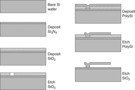
Surface micromachining refers to processes that fabricate the mechanical structure on the surface of the silicon wafer. A basic example process based upon a sacrificial layer is shown in Fig. 10.1. A thin layer of silicon nitride (Si3N4) is deposited onto a bare silicon wafer. This acts to protect the wafer and electrically isolate the subsequent layers from the substrate. Next, a layer of silicon dioxide (SiO2) is deposited onto the nitride layer. The SiO2 film is the sacrificial layer in this process and its thickness determines the final gap between the structure and the substrate. The SiO2 layer is patterned using photolithography and etched with a simple liquid chemical etchant (hydrofluoric acid, HF) or by plasma etching. This etching process removes part of the SiO2 film exposing the nitride layer beneath. These exposed features form the anchor points of the mechanical structure and their location and geometry will depend upon the mechanical deign of the structure. Next, the material that will form the mechanical structure is deposited onto the wafer. This material should have good mechanical properties and polysilicon is a common choice. The thickness of the polysilicon film determines the thickness of the mechanical structure. This mechanical polysilicon layer is patterned by photolithography and selectively removed using a plasma etch. This step transfers the mechanical design to the polysilicon layer. Finally, the silicon dioxide layer is ‘sacrificed’ by removing it completely with an appropriate etch. This leaves the mechanical structure freestanding on the top surface of the silicon wafer.
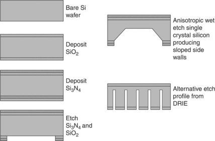
Bulk micromachining refers to processes that result in the mechanical structure being fabricated from the single crystal silicon wafer itself, rather than on top of it. This requires etching processes that selectively etch exposed regions of the silicon wafer. An example process is shown in Fig. 10.2. The wafer is protected by films of materials that resist the etch process. For example, in the case of potassium hydroxide (KOH) etch, silicon nitride is used together with a stress-absorbing SiO2 film. These films are patterned using standard photolithographic techniques and etched to expose the single crystal silicon substrate below. In the case of a wet etch such as KOH, the wafers are simply immersed in the etchant for the required length of time and the exposed silicon is removed at a rate of approximately 0.7 μm/min. KOH is an anisotropic etch, which means the etch rate varies with crystalline direction. The {111} crystal planes are virtually untouched by KOH, which leaves the characteristic sloped side walls shown in Fig. 10.2. The angle of the slope to the surface of the wafer is 54.7 degrees. More recently, a plasma silicon etch known as deep reactive ion etching (DRIE) has been developed for bulk micromachining. The DRIE process is capable of etching the silicon at rates in excess of 10 μm/min, only requires photoresist as a masking material and etches near vertical sidewalls enabling high aspect ration structures to be formed. An example DRIE etch profile is also shown in Fig. 10.2.
10.2.2 Process considerations for thick-film silicon MEMS
The compatibility of printed thick-films with various micromachining steps is a key issue for identifying a complete process whereby these films can be used with mechanical microsystems (Beeby et al., 1999). One difficulty associated with the thick-film printing process is the pressure applied to the substrate during the printing process. The mechanical structure upon which the PZT is to be printed must be of sufficient strength to withstand this pressure. A second difficulty is the accuracy of registration of the printed layers with respect to micromachined structures and layers patterned using standard photolithographic techniques. The registration accuracy of thick-film layers printed using typical processing equipment is ± 50 μm, which is relatively poor compared to photolithography. The effect of both these restrictions can be reduced or overcome if the thick-film printing processes are carried out first, followed by the silicon micromachining. This results in the printing steps being carried out on a partially etched or even completely un-etched silicon wafer. The subsequent micromachining processes could, where applicable, be aligned to the printed layer, thereby improving registration.
This approach requires the printed PZT film to survive the subsequent etching, photolithographic steps and deposition processes. An investigation into the compatibility issues of micromachining silicon wafers with PZT layers printed on the surface has been completed by Beeby et al. (1999). This work studied in particular the interaction and adhesion between the printed films and the substrate and the effects of exposure to various micromachining processes.
Interfacial reactions
Printed thick-film PZT layers typically require firing at temperatures in excess of 850 °C, and this causes a problem when the films are printed on silicon due to migration of lead (Pb) atoms from the PZT into the silicon (Beeby et al., 1999, Maas et al., 1997). This migration results in a reaction between the lead and the silicon forming lead silicate compounds at the silicon/film interface. This reaction can cause delamination of the bottom thin film electrode and printed film, and increased conductivity of SiO2 passivation layers. This increased conductivity can cause short circuits between electrodes and care has to be taken to ensure these are sufficiently physically separated. An example reaction is shown in Fig. 10.3. This migration is unaffected by standard passivation layers such as SiO2 and Si3N4, with the Pb diffusing easily through these layers.
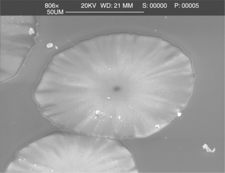
10.3 Example reaction between lead from the PZT and silicon substrate after firing at 900 °C for 1 hour.
One method of avoiding this is to deposit a diffusion barrier between the printed PZT and the substrate. The diffusion barrier should prevent the Pb atoms reaching the Si substrate whilst being as thin as possible and have sufficient adhesion to both the substrate and the subsequently deposited/printed films (Dorey and Whatmore, 2005). Example diffusion barriers include thin-film (70 nm thick) yttria-stabilised zirconia (YSZ) plus 30 nm titanium dioxide (TiO2), 120–150 nm zirconium oxide (ZrO2), 350 nm TiO2, or thick-film layers of YSZ (1 μm), 1 μm SiO2/50 nm TiO2/0.5 μm platinum (Pt) (Dorey and Whatmore, 2005).
Compatibility with micromachining processes
Micromachining processes are required either to selectively etch the substrate, thereby forming the micromechanical structure or to pattern the printed film itself. Given the overall fabrication process described above, it is clearly necessary to etch the silicon substrate or the various deposited films using a process that does not affect the printed film or electrode layers. It is not possible to protect printed thick-films using a photolithographic process because the topology of a printed wafer prevents spin coating resist layers with even thicknesses. Standard wet (liquid) and dry (plasma) etches were evaluated by Beeby et al. (1999) in order to identify suitable methods. Wet etches were found not to be suitable. For example, a common wet anisotropic KOH etch was found to reduce the adhesion of the electrode and PZT films causing the printed areas to float away. Similarly, a wet-buffered hydrofluoric acid (BHF) (a SiO2 etch) also reduced the adhesion of the printed film. Plasma-based etches, however, were found to have little affect on the printed films or bottom electrode. For example, a sulphur hexafluoride (SF6) reactive ion etch (RIE), which is a semi-anisotropic Si etch, was found to remove the Si at up to 1 μm a minute depending upon the area of exposed silicon. Depending upon the presence of any reaction material, a short SiO2 plasma etch based upon CHF3 may be required beforehand to remove the lead silicate.
10.2.3 Example silicon/thick-film MEMS
A number of different mechanical sensors have been fabricated in silicon and the final fabrication processes developed for these devices highlight the details discussed above.
The first of these is a micromachined silicon micropump fabricated with a thick-film PZT actuator (Koch et al., 1998). The pump, shown in Fig. 10.4, consists of a thin silicon membrane with a thick-film PZT actuator printed on the top surface. This structure is bonded to two other wafers, which form the cantilever valves that control the direction of the fluid flow through the pump. The PZT actuator is activated in one direction causing the membrane to move upwards increasing the volume in the pump chamber and drawing fluid in through the inlet. The actuator is then connected with the opposite polarity, causing the membrane to move down, reducing the chamber volume and forcing the fluid out through the outlet. The device was fabricated by first micromachining the membranes and then printing the PZT and electrode films. This approach highlighted the difficulty of printing onto fragile structures. In this case, the 8 mm × 4 mm diaphragm of the micropump was found to fracture during printing if its thickness was less than 60 μm. The pump proved successful in achieving rates of up to 120 μl min− 1 but did require a 600 Vpp driving voltage.
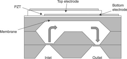
10.4 Silicon micropump with printed thick-film piezoelectric actuation (piezoelectric layer 100 μm thick).
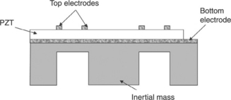
The next device is a bulk micromachined silicon accelerometer with thick-film PZT elements for sensing the deflections of the inertial mass (Beeby and White, 2001). The device structure is shown in Fig. 10.5 and it demonstrates a fabrication process that overcomes the fragility of the microstructure. It consists of a square inertial mass supported at each corner by a thin silicon beam with the printed thick-film PZT located on the top surface of each beam. As the inertial mass vibrates in and out of the plane of the wafer, the supporting beams deflect and the PZT becomes strained hence generating a charge output. The final device shown in Fig. 10.5 is clearly very fragile and would not survive the physical nature of the screen-printing process. The following process, shown in Fig. 10.6, describes the approach taken to overcome this.
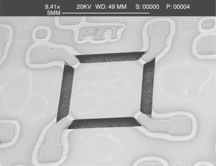
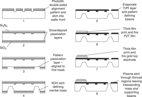
Double-polished, 525 μm thick, type < 100 > silicon wafers were first patterned using a standard double-sided photolithography process to enable processes carried out on both sides of the wafer to be aligned. The double-sided alignment pattern on the top side also included the chip frame and 1 mm2 alignment aids for the thick-film printing steps. Next, KOH masking layers (600 nm SiO2 and 160 nm Si3N4) were grown/deposited on both sides of the wafers. These layers were then patterned on the back wafer surface to define the inertial mass using a double-sided alignment process to locate the inertial mass at the centre of the chip. The passivation layers were etched using a resist mask and a CHF3 + Ar plasma, after which the resist was removed. The wafers were then immersed in agitated KOH at 70 °C for 13 hours, sufficient to etch down to a depth of 480 μm. This etched a trench around the square inertial mass leaving a thin membrane 40 μm thick and 660 μm wide. The KOH etch has to be performed before printing since the PZT and electrodes cannot withstand this etch. The SiO2 and Si3N4 passivation layers were stripped and the bottom electrode (500 nm Pt + 50 nm Ti) was deposited using an e-beam evaporator. This electrode combination was previously found to be unaffected by an SF6 plasma etch (Beeby et al., 1999), and could therefore be used as the masking layer for the final etch that defines the beams and releases the inertial mass. The bottom electrode was patterned with a 1.7 mm thick hardbaked layer of resist sufficient to withstand a 12-minute ion beam mill. The layer of resist was then stripped and the substrates prepared for the thick-film printing process. Since the inertial mass was at this stage only supported by a 40 μm thick membrane, additional support was required. This was achieved by bonding the substrate to a host wafer using a thin layer of resist. The host wafer supports the inertial mass during the printing process and protects the etched substrate against the vacuum chuck used by the thick-film printer. Once supported in this manner, the membranes were found to comfortably withstand the pressure exerted during the printing process. The PZT paste was printed through a stainless steel screen with the screen aligned to the 1 mm2 features defined in the top surface during step 1. This positioned the PZT elements on the bottom electrodes that define the supporting beams. Two print strokes yielded a thickness of approximately 60 μm after drying and firing at 890 °C for 1 hour, which has been found to sinter the particles adequately without resulting in too much lead loss or reaction. A gold cermet ink, ESL 8836, was printed on the top of the PZT and fired at 890 °C, leaving an approximate thickness of 10 μm. Due to the reaction increasing the conductivity of the oxide, the top electrode was located entirely on the top surface of the PZT and accurate alignment between printed layers was essential to prevent short circuits between the top and bottom electrodes.
The final process involves plasma etching from the front of the wafer through the silicon membrane, with the bottom electrode being used as the masking layer to define the final structure. Given the presence of the reaction material, a CHF3 + Ar etch for 1 hour was first performed, which cleaned the surface prior the silicon etch. An SF6 silicon etch for 80 minutes was sufficient to etch through the membranes across the entire wafer, leaving the inertial mass supported by the four beams with the PZT sensing structure already in place on the top surface of each beam. The wafers were once more resist bonded to a host wafer to support the device during dicing. Once sawn, the individual chips were freed from the host wafer by soaking in acetone before being packaged for testing. The yield of this process was excellent, with 97% of devices in the first batch of this kind being successfully fabricated and diced.
Despite being designed primarily to demonstrate the feasibility of the fabrication process, the accelerometer functioned correctly with a flat frequency response up to its first resonant peak at 7.5 kHz. The accelerometer was also used to demonstrate a self-test procedure, where three of the piezoelectric elements were used to excite the inertial mass allowing the operation of the fourth element in the sensing mode to be confirmed (Beeby et al., 2001).
This fabrication process was also used by Beeby and White (2001) to demonstrate the use of screen-printed piezoelectric elements to drive and detect the vibrations of a resonant silicon MEMS beam. Whilst the resonator was not implemented as a sensor, the piezoelectric elements worked well successfully driving the beam into resonance at 56.5 kHz. This work led to the incorporation of printed piezoelectric films on a stainless steel triple beam tuning fork (TBTF) resonator that was employed as a strain gauge (Yan et al., 2004). This device is designed to be used as an alternative to a traditional resistive strain gauge and was therefore quite large (45 mm long, 7 mm wide).
Screen-printed piezoelectric films for silicon MEMS have also been studied by a collaboration between Ferroperm Piezoeceramics A/S (now part of the Meggitt Group) and the Technical University of Denmark. They have developed a commercially available screen-printable piezoelectric material called INSENSOR TF2100, which is based upon Ferroperm Pz26 material, and have combined this with silicon to make a variety of accelerometers. One design is very similar to the device shown in Fig. 10.5 but with a different electrode arrangement and fabricated using an advanced silicon etch process which is a fast etch that gives high aspect ratio structures with vertical sidewalls (Lou-Moeller et al., 2007). Another version developed by the same team places the supporting beams midway along the length of the inertial mass rather than at the corners, and the volume occupied by the mass is maximised to improve sensitivity (Hindrichsen et al., 2006). In this case, the micromachining process is completed before printing and the device was found to withstand the printing process, provided that the beams were not thinner than 20 μm. This device demonstrated a sensitivity of 4.15 mV/g.
This team has continued to work on accelerometers and has demonstrated a circular device with the advantage that features are not etched completely through the wafer (Hindrichsen et al., 2009). A cross-section is shown in Fig. 10.7 and this design simplifies printing and mechanically reduces off-axis cross sensitivity. The top electrodes are arranged as rings about the periphery of the annular membrane. This is the location of the maximum stresses, which will be of opposite sign during operation. Therefore the inner and outer rings are polarised in opposite directions to compensate for the opposite stresses. The PZT is printed across the device apart from openings that allow access to the SiO2/Ti/Pt barrier layer and bottom electrode. The PZT film is 24 μm thick and is sintered at 850 °C. The top electrode is a 400 nm thick platinum (Pt) film patterned using a lift off process. The device works well as a uniaxial accelerometer and has a wide operating bandwidth due to the high resonant frequency of 23.5 kHz.
The most recent work by this team has demonstrated a triaxial MEMS accelerometer (Hindrichsen et al., 2010). The device is similar to the previous design with a square inertial mass supported by beams located at the mid point of the sides of the mass. By analysing the output of each bean independently, accelerations in three axes can be detected. The accelerometers are fabricated using silicon on insulator (SOI) wafers with the depth of the buried oxide determining the thickness of the beams. The disparity between the resolution of the MEMS process and the printing step is overcome by first etching through the wafer to define the beams. The printed pattern is designed to overlap the edges of the beams, but since the substrate has been removed the material remains on the screen and the resolution effectively becomes the same as for the etch process. However, this approach does not work perfectly since some PZT overhangs of differing dimensions were left and these affected the performance of the device.
Other work on screen-printed piezoelectric layers have avoided the difficulties of the high firing temperatures on silicon by using a laser transfer method (Xu et al., 2005). The thick-film PZT was printed onto a sapphire substrate, dried at 80 °C for 10 minutes and then fired at 1200 °C for 2 hours in a Pb-rich atmosphere. The PZT elements were polished and a thin-film Chrome/Gold (200 Å Cr/5000 Å Au) electrode was evaporated onto the top of the PZT. The PZT elements were bonded to a Pt-coated silicon wafer using conductive silver epoxy. The PZT elements were then exposed to an XeCl excimer laser with 308 nm wavelength and 700 mJ/cm2 fluence, which releases them from the sapphire substrate. Another Cr/Au film was deposited onto the PZT using a shadow mask to define the pattern. This approach leaves a very dense film with higher dielectric constants than standard thick-films and improved piezoelectric properties. The challenge with this approach would be in aligning the two substrates prior to bonding and achieving a good quality epoxy bond across the entire PZT surface.
10.3 Printed films with ceramic MEMS
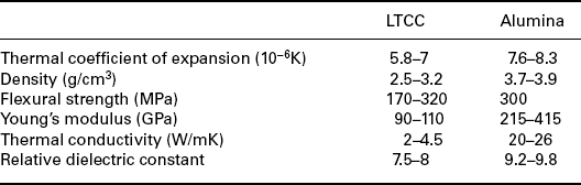
Compared with silicon, ceramic substrates offer the advantage of less aggressive interactions with thick-film materials and particularly with PZT films fired at high temperatures. The most common ceramic substrate material is aluminium oxide (Al2O3), better known as alumina, which is very limited in terms of bulk micromachining options compared with silicon and can only be cut by laser machining. Due to this limitation, alumina is typically used as a substrate for surface-micromachined structures. Low-temperature co-fired ceramics (LTCCs) are designed to be fired simultaneously with printed passive components, such as resistors, inductors and capacitors, at temperatures below 1000 °C. LTCC substrates are typically stacked on top of each other, laminated under pressure and co-fired to give a multilayer substrate for use with hybrid circuits and multi-chip modules. LTCC is formed from alumina and glass powders and in its green state (unfired) it is much softer than alumina and can be cut and drilled by conventional machining, laser micromachined or even embossed using micromachined nickel tools (Andrijasevic et al., 2007). The ability to stack and bond layers of machined LTCC offers the capability to realise mechanical microstructures suitable for use with thick-film materials for both sensing and actuating applications. A comparison between alumina and LTCC is given in Table 10.1.
10.3.1 Surface-micromachined ceramic MEMS
In this class of devices, the alumina is used simply as a supporting substrate for free-standing micromechanical structures fabricated onto the top surface. A variety of processes for different applications have been developed, but they are all based upon the sacrificial process illustrated in Fig. 10.1. The following devices are all examples that highlight the capabilities of this approach and the range of applications that have been demonstrated.
The first is a ceramic capacitive pressure sensor designed for high-temperature applications (Sippola and Ahn, 2006). Screen printing has been used to deposit the top and bottom electrodes, the ceramic structural layers and the thick-film sacrificial layer. These layers have been printed onto an alumina substrate that has vias pre-laser drilled through the thickness that allow access for the chemical etchant that removes the sacrificial layer, as illustrated in Fig. 10.8. The gold bottom electrode was screen-printed first and this is patterned to avoid the vias. Next, a standard thick-film dielectric was printed to protect the electrode layer. The third printed layer is a gold film that acts as the sacrificial layer, and the dielectric and top electrode layers are than printed on top of this. The gold sacrificial film is removed by a liquid gold etch leaving a 4.8 mm × 2.8 mm, 32 μm thick diaphragm with a 22 μm thick gap between the electrodes. Finally, a dielectric layer is printed on the back of the alumina to seal the vias. The paper claims that the mechanical properties of the printed dielectric structure are superior to LTCC, and highlights the flexibility offered by the process that enables the gap height to be defined by the thickness of the sacrificial layer. The sensor proved to be hermetic after firing and demonstrated sensitivities up to 21.9 fF/psi at room temperature and 10 fF/psi at 300 °C.
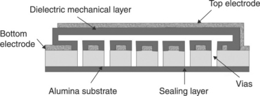
10.8 Ceramic capacitive pressure sensor by Sippola and Ahn, 2006.
One disadvantage of the previous device is the cost associated with a gold sacrificial layer. An alternative approach is to use strontium carbonate (SrCO3) powder in an epoxy matrix (Lucat et al., 2008). The epoxy will have decomposed by 450 °C but the SrCO3 can withstand temperatures up to 900 °C and this is simply removed by a weak phosphoric acid aqueous solution. This process has been used to demonstrate a range of printed devices and structures including cantilever force sensors (Lakhmi et al., 2010), micro-channels and an electrothermal actuator (Ginet et al., 2007).
A much more complex surface micromachining approach was developed by Suzuki et al. (2009) in the fabrication of a micro accelerometer. This used a screen-printed barium titanate (BaTiO3) film on a platinised alumina substrate. Amorphous silicon, used as the sacrificial layer, was then vapour deposited on top, patterned and etched. This was followed by the deposition and patterning of Parylene, aluminium and a second Parylene layer. The exposed amorphous silicon was then removed by a plasma etch to leave the free-standing inertial mass. It is clear that most of this process is based upon conventional silicon micromachining steps and only the BaTiO3 is actually screen-printed.
The final example of a free-standing microstructure printed on an alumina substrate is a piezoelectric cantilever designed for vibration energy harvesting (Kok et al., 2009). In this work, the sacrificial layer is a printed carbon film that burns out at temperatures above 800 °C. A variety of combinations of electrodes and PZT films were screen-printed over the top of the carbon layer, after which the films were co-fired thereby sintering the films and removing the sacrificial layer. A maximum power output of 40 μW was measured when the harvester was shaken at the cantilever’s resonant frequency of 400 Hz and an acceleration level of 0.5 g (1 g = 9.81 m/s2). Energy harvesting is a topic receiving a great deal of interest at the moment. For a device to be successful it should operate at a target frequency specified by the application and the mass should be maximised to increase the power output. The device should also be robust and operate unchanged for many years. It is not clear if these attributes are achievable with this process or mechanical structure.
10.3.2 Low temperature co-fired ceramic MEMS
The use of LTCC to fabricate microstructures is an established process, with the first devices being demonstrated in the late 1990s. Whilst it offers many advantages in terms of the geometries that can be achieved, restrictions include the limitations on some dimensions (i.e. thicknesses and gaps) by dried tape thickness, which is prescribed by the manufacturer. Also, the mechanical properties are limited to those of the fired film, which are certainly inferior to silicon.
An early example is a capacitive pressure sensor designed to operate wirelessly in high-temperature applications (Fig 10.9) (Fonseca et al., 2002). The sensor is made from three layers of LTCC, with the outer layers being 0.1 mm thick. The centre spacer layer has a circular hole cut in it with a radius of 4.2 mm. The silver top electrode is printed inside a coil inductor and a silver bottom electrode is printed on the bottom layer. The three layers are laminated together in a hot vacuum press and subjected to 3000 psi at 70 °C and then diced up to leave the individual sensors. These are fired in air for 30 minutes at 500 °C and then 20 minutes at 850 °C, which hardens the LTCC and fires the ink. The capacitor and inductor form a resonant LC circuit, the frequency of which depends upon the capacitance, which in turn depends upon the applied pressure. The sensor can be interrogated remotely and was found to operate up to 400 °C and over a pressure range of 7 Bar.
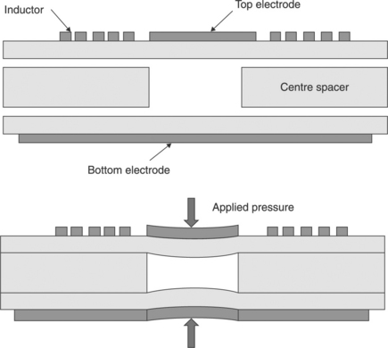
10.9 LTCC capacitive pressure sensor (after Fonseca et al., 2002).
Other sensing mechanisms have also been evaluated on LTCC by the research team at the Jozef Stefan Institute in Slovenia. They compared thick-film resistors, which act as a strain gauge producing a change in resistance when strained, on alumina, pre-fired and co-fired LTCC (Belavic et al., 2007). The resistivity and thermal coefficient of resistance were found to vary between the substrates, but the amount of variation depends upon the resistive ink used. The gauge factor remains largely unaffected, with the LTCC resistors being marginally less sensitive than the alumina case. They also compared PZT thick-films on the same range of substrates and found that the level of piezoelectric activity on LTCC was around 50% that of the value found on alumina. This was thought to be due to reactions between the silica in the LTCC and the lead in the PZT.
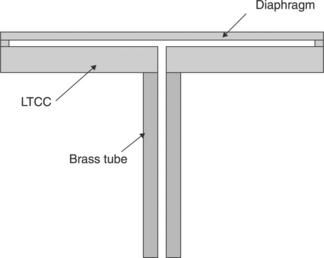
The same group have also demonstrated an LTCC piezoresistive pressure sensor illustrated in Fig. 10.10. The diaphragm had a diameter of 26 mm and a thickness of 0.2 mm, with four piezoresistors printed in the standard layout for diaphragm pressure sensors with two in the centre and two on the edge. The holes where first cut by laser machining and the assembly laminated at 875 °C. The sensors functioned well in the intended low pressure regime but the offset voltage did exhibit a large temperature dependence of 30–80 μV/K.
The most impressive demonstration of the capability of the LTCC assembly process for microstructures is demonstrated by a solid propellant-based micro thruster (Thakur et al., 2010). Features were laser machined and then up to eight patterned layers were laminated together to form the final structure. The laminated assembly forms a 420 mm thick cavity with an exhaust nozzle located at the side of the chamber. The thick-film aspect of this device is routine, with a screen-printed resistor being located in the chamber for ignition purposes. The conductive tracks and wire bond pads were printed using DuPont 6146 Ag/Pd paste, whilst the resistors were formed from DP 5092D or DP CF011 compositions. After filling with suitable propellant, this was ignited by the thick-film heater, producing an average thrust of 19.5 mN for 150 ms.
10.4 Conclusion and future trends
Thick-film materials will continue to be a niche process within MEMS that does offer some useful advantages but also suffers some drawbacks. Thick-films often offer improved material properties compared to their thin-film counterparts and also benefit from a very simple low-cost printing deposition process. The drawbacks include the reactions that can occur when printing on silicon, the relatively poor resolution achievable compared to photolithography and the physical nature of the printing process. The properties of some printed materials, such as piezoelectrics, are also inferior to their bulk counterpart, which will reduce the performance of the MEMS device.
These challenges are being addressed and further improvements can be expected with time. Printed piezoelectric film properties, for example, are being improved by increasing the densification and reducing the porosity of the films. The use of nano-size particles to reduce firing temperatures is also an avenue of research, with attention being paid to grain growth during sintering. Alternative printing processes are another area where significant improvements could be obtained that radically increase the use of printed films in MEMS. Digital printing techniques such as ink-jet printing are attractive because they are non contact and do not require a screen. The challenge with ink-jet printing is achieving inks loaded with enough active material to demonstrate useful film properties whilst maintaining the rheology required for the ink-jet process. The viscosity requirements for ink-jet inks are much lower than for screen printing and therefore the inks cannot contain the same concentration of active particles possible in an ink developed for screen printing. Ink-jet printing is also not well suited to achieving thick-printed films: numerous prints are required to build up film thicknesses.
One printing technique that offers the benefits of digital printing without the rheological constraints on the inks is dispenser printing. This involves the use of a pneumatically driven syringe and a computer-controlled x, y, z stage to deposit inks in the pattern required. It is non-contact, does not require a screen and can print existing thick-film inks without modification. Another significant advantage is the potential increase in resolution. Syringe nozzles are available with 1 μm diameter orifices offering the potential for a pattern resolution comparable with most MEMS microstructures.
10.5 References
Andrijasevic, D., Smetana, W., Zehetner, J., Zoppel, S., Brenner, W., Aspects of micro structuring low temperature co-fi red ceramic (LTCC) for realisation complex 3D objects by embossing. Proceedings of the 32ndInternational Conference on Micro- and Nano-Engineering, May – August 2007, pp. 1198 – 1201. Microelectronic Engineering 2007; 84:5–8.
Beeby, S.P., White, N.M. Silicon micromechanical resonator with thick-film printed vibration excitation and detection mechanisms. Sensors and Actuators A: Physical. 2001; 88:189–197.
Beeby, S.P., Blackburn, A., White, N.M. Processing of PZT piezoelectric thick-films on silicon for microelectromechanical systems. Journal of Micromechanics and Microengineering. 1999; 9(3):218–229.
Beeby, S.P., Grabham, N.J., White, N.M. Microprocessor implemented self validation of thick-film PZT/Silicon accelerometer. Sensors and Actuators A: Physical. 2001; 92:168–174.
Belavic, D., Hrovat, M., Holc, J., Zarnik, M.S., Kosec, M., et al. The application of thick-film technology in C-MEMS. Journal of Electroceramics. 2007; 19(4):363–368.
DeVoe, D.L. Piezoelectric thin film micromechanical beam resonators. Sensors and Actuators A: Physical. 2001; 88(3):263–272.
Dorey, R.A., Whatmore, R.W. Ceramic thick-films for MEMS. In: Setter N., ed. Electroceramic-based MEMS. New York: Springer; 2005:177–197.
Fonseca, M.A., English, J.M., von Arx, M., Allen, M.G. Wireless micromachined ceramic pressure sensor for high-temperature applications. Journal of Microelectromechanical Systems. 2002; 11(4):337–343.
Ginet, P., Lucat, C., Ménil, F., Battaglia, J.-L. Modelling and characterizing a screen-printed metallic electrothermal microactuator. International Journal of Applied Ceramic Technology. 2007; 4:423–427.
Hindrichsen, C.C., Almind, N.S., Brodersen, S.H., Lou-Moeller, R., Hansen, K., et al. Triaxial MEMS accelerometer with screen-printed PZT thick-film. Journal of Electroceramics. 2010; 25:108–115.
Hindrichsen, C.C., Larsen, J., Thomsen, E.V., Lou-Moeller, R., Hansen, K. Circular piezoelectric accelerometer for high band width application. Proceedings of IEEE Sensors Conference, Christchurch, NZ, October 25–28. 2009; 475–478.
Hindrichsen, C.C., Thomsen, E.V., Lou-Moeller, R., Bove, T. MEMS accelerometer with screen-printed piezoelectric thick-film. Proceedings of IEEE Sensors Conference, Korea, October 22–25. 2006; 1477–1480.
Hrovat, M., Belavic, D., Ursic, H., Kita, J., Holc, J., et al. An investigation of thick-film materials for temperature and pressure sensors on self-constrained LTCC substrates. 2008:339–346.
Ko, S.C., Kim, Y.C., Lee, S.S., Choi, S.H., Kim, S.R. Micromachined piezoelectric membrane acoustic device. Sensors and Actuators A: Physical. 2003; 103(1–2):130–134.
Koch, M., Harris, N., Evans, A.G.R., White, N.M., Brunnschweiler, A. A novel micromachined pump based on thick-film piezoelectric actuation. Sensors and Actuators A: Physical. 1998; 70:98–103.
Kok, S.-L., White, N.M., Harris, N.R. Fabrication and characterisation of free-standing thick-film piezoelectric cantilevers for energy harvesting. Measurement Science and Technology. 2009; 20:124010.
Lakhmi, R., Debeda, H., Dufour, I., Lucat, C. Force sensors based on screen-printed cantilevers. IEEE Sensors Journal. 2010; 10(6):1133–1137.
Lou-Moeller, R., Hindrichsen, C.C., Thamdrup, L.H., Bove, T., Ringgaard, E., et al. Screen-printed piezoceramic thick-films for miniturised devices. Journal of Electroceramics. 2007; 19:333–338.
Lucat, C., Ginet, P., Castille, C., Debeda, H., Menil, F., Microsystems elements based on free-standing thick-films made with a new sacrificial layer process. Microelectronics Reliability, 48, 6, Thermal, Mechanical and Multi-physics Simulation and Experiments in Micro-electronics and Micro-systems (EuroSimE 2007). 2008:872–875. [June].
Maas, R., Koch, M., Harris, N., Evans, A., White, N. Thick-film printing of PZT onto silicon. Materials Letters. 1997; 31:109–112.
Marzencki, M., Ammar, Y., Basrour, S. Integrated power harvesting system including a MEMS generator and a power management circuit. Sensors and Actuators A: Physical. 2008; 145–146:363–370.
Sippola, C.B., Ahn, C.H. A thick-film screen-printed ceramic capacitive pressure microsensor for high temperature applications. Journal of Micromechanics and Microengineering. 2006; 16:1086–1091.
Suzuki, M., Kobayashi, Y., Aoyagi, S., Tajiri, H., Nagahata, T., Micro accelerometer using screen-printed BaTiO3 film on ceramic substrate. Proceedings of 15th International Conference on Solid-State Sensors, Actuators and Microsystems. 2009:1174–1177. [Transducers 2009, Denver, CO, USA].
Thakur, J., Pratap, R., Fournier, Y., Maeder, T., Ryser, P. Realization of a solid-propellant based microthruster using low temperature co-fired ceramics. Sensors and Transducers Journal. June 2010; 117(6):29–40.
Trolier-McKinstry, S., Muralt, P. Thin film piezoelectrics for MEMS. In: Setter N., ed. Electroceramic-based MEMS. New York: Springer; 2005:199–215.
Xu, B., White, D., Zesch, J., Rodkin, A., Buhler, S., et al. Characterisitics of lead zirconate titanate ferroelectric thick-films from a screen-printing laser transfer method. Applied Physics Letters. 2005; 87:192902.
Yamashita, K., Katata, H., Okuyama, M., Miyoshi, H., Kato, G., et al. Arrayed ultrasonic microsensors with high directivity for in-air use using PZT thin film on silicon diaphragms. Sensors and Actuators A: Physical. 2002; 97–98:302–307.
Yan, T., Jones, B.E., Rakowski, R.T., Tudor, M.J., Beeby, S.P., et al. Development of metallic digital strain gauges. Measurement and Control. 2004; 37(7):214–216. [10.6 Complete micromachining process for the silicon/thick-film PZT accelerometer].