
2.2
The Photophysics of Halide Perovskite Solar Cells
Mingjie Li Bo Wu and Tze‐Chien Sum
Nanyang Technological University, Division of Physics and Applied Physics, School of Physical and Mathematical Sciences, 21 Nanyang Link, SPMS‐PAP‐03‐05, Singapore, 637371, Singapore
2.2.1 Introduction to Photophysics Studies of Halide Perovskites
The rapid transcendence of organic‐inorganic lead halide perovskites to prominence is unprecedented in the annals of photovoltaic (PV) history. In less than a decade, the efficiencies of these amazing perovskite solar cells have bounded from a mere 3.8% in 2009 to 22.1% in 2016. Despite the great strides made with the device efficiency, the detailed understanding of halide perovskite's fundamental photophysics remains modest. To realize the full potential of these perovskite solar cells, both basic characterization and device optimization studies need to progress synchronously to gain a complete picture of their fundamental photophysical and optoelectronic properties. A wide array of optical spectroscopy techniques is available to the spectroscopist to characterize the optical properties and probe the charge dynamics of these materials and devices. These techniques range from the ubiquitous absorption spectroscopy to more sophisticated pump‐probe techniques of transient absorption (TA), spectroscopy terahertz (THz) spectroscopy, and photoconductance spectroscopy. The operating principles of these techniques are not covered here, and the interested reader is directed to other excellent articles on them. In this chapter, we first discuss the basic optical properties of polycrystalline halide perovskite thin films, followed by the charge dynamics of these bare films and the interfacial charge‐transfer mechanisms at the heterojunctions of perovskite solar cells. Lastly, we discuss the photophysical properties of perovskite single crystals (SCs) and their potential for perovskite optoelectronics.

Figure 2.2.1 (a) Electronic band structure of cubic MAPbI3 calculated from density functional theory with spin–orbit coupling [1]. Gray upward arrows indicate the allowed transitions in the visible range. The upward arrows at the R point represent the possible transitions corresponding to the higher absorption energies. (b) Room temperature absorption coefficient of polycrystalline MAPbI3 thin film as a function of photon energy. Representative PL spectra at ∼1.6 eV that arises from carrier recombination near the R valley (dashed line) in (a).
Source: (a) Even et al. 2014 [1]. Copyright 2014. Reprinted with permission of American Chemical Society. (b) Xing et al. 2013 [2]. Copyright 2013. Reprinted with permission of the American Association for the Advancement of Science.
2.2.2 Optical Properties of CH3NH3PbI3 Polycrystalline Thin Films
2.2.2.1 Electronic Band Structure and Optical Transitions
The photophysics and charge carrier dynamics in semiconductors is highly dependent on their electronic band structures. We begin with considering the band structure of organic–inorganic lead halide perovskites (e.g. methylammonium lead iodide – CH3NH3PbI3 or simply MAPbI3 in short), which had been subjected to extensive theoretical calculations by many groups. Figure 2.2.1a shows the representative calculated band structure of cubic MAPbI3 near the R point by the density functional theory (DFT) method with spin–orbit coupling included [3]. The cubic MAPbI3 presents a direct bandgap where the valence band maximum (VBM) and conduction band minimum (CBM) occur at almost the same point in the Brillouin zone. Similarly, the tetragonal and orthorhombic phases of MAPbI3 are also direct semiconductors with bandgaps comparable to the cubic phase. Despite the organic constituents, MAPbI3 retains its inorganic semiconductor characteristics, with the CBM almost entirely composed of Pb p orbital with negligible coupling with I, while the VBM comprised the antibonding states derived from the hybridization of the I 5p‐ and Pb 6s states. The strong s–p antibonding coupling results in a small‐hole effective mass which is comparable with the electron effective mass, making MAPbI3‐based perovskites an ideal candidate for thin‐film p‐i‐n solar cells.
The optically allowed transitions (E 1/2,u → E 1/2,g) at R represent the bandgap energy that is evident from the strong absorption onset at ∼1.6 eV (see Figure 2.2.1b). MAPbI3 also possesses a fairly large absorption coefficient (>105 cm−1 at ∼2.5 eV or ∼500 nm – see Figure 2.2.1b) [2], which is comparable to CdTe and GaAs and is approximately one order higher than crystalline Si. The charge carriers photoexcited by the wide range of visible light can subsequently relax into the R valley from the M point. These transitions would account for the absorption continuum for photon energies >1.6 eV band edge. Furthermore, Even et al. proposed that the absorption edge at ∼2.6 eV arise from the optically allowed transitions at the R point, involving transitions from the deeper energy levels to the CBM or from the VBM to the higher energy states (see vertical arrows in Figure 2.2.1a). Eventually, the relaxation of carriers at the R valley from CBM to VBM would give rise to a photoluminescence (PL) peak near 1.6 eV.
2.2.2.2 Exciton Binding Energies and Photoexcited Species: Excitons Versus Free photo-excited species"?> Carriers
Knowledge of the dominant photoexcited species in perovskites is essential for a clear understanding of the working principles of perovskite solar cells. One possible clue to whether the primary species is a free carrier or a bound electron–hole pair lies in the value of the exciton binding energy E b. However, this is not entirely straightforward as a puzzling range of the exciton binding energies (E b) soon emerged (i.e. <10 to ∼50 meV) from the sustained efforts to identify the primary photoexcited species (excitons or free carriers) in MAPbI3 [4–6]. These attempts are also greatly frustrated by the various experimental techniques used – ranging from optical absorption [7] and magnetoabsorption [8] to temperature‐dependent PL [9, 10] and temperature‐dependent absorption spectroscopy [4], etc., which contribute to the spread of exciton E b. It is therefore difficult to conclude if the primary photoexcited species in these perovskites at room temperatures are excitons (insulating) or free carriers (conducting). MAPbI3 differs from typical semiconductors such as CdS (E b ∼ 26 meV) which has dominating excitonic properties at room temperatures [11]. A coexistence of both species in thermal equilibrium at room temperatures seems plausible based on the E b value alone. This coexistence picture is consistent with the findings of Vardeny's group, where evidence of both excitons and photogenerated carriers with an estimated branching ratio of 1 : 10 through pump‐probe spectroscopy were presented [12].
Using femtosecond pumped transient THz spectroscopy, Sundstrom's group provided the first evidence that free charge carriers are generated within 2 ps in MAPbI3 and MAPbI3/me‐Al2O3 thin films [13]. These findings concur with the Drude‐like free‐carrier responses from transient THz spectroscopy studies of perovskites by Herz's group [14]. Furthermore, the dominant free electron and free hole bimolecular recombination were evidenced by several groups [10, 15–17] over a wide range of photoexcited charge carrier concentration through ultrafast spectroscopy techniques (e.g. time‐resolved THz, TA, and time‐resolved photoluminescence (TRPL)). Direct measurements of the exciton binding energies using high magnetic fields eventually revealed binding energies <16 meV at low temperatures and a few milli‐electron volts at room temperature (within the detection limits of the technique). Eventually, Petrozza's group [4] clearly showed that the grain size of the perovskite crystallites strongly affects the excitonic properties. The resulting surface‐induced structural changes and doping could reduce the E b. Hence, the broad spread of E b found in the literature could be rationalized to be due to not only from the experimental uncertainties in the various measurement approaches, but, more importantly, from the strong dependence on the perovskite film processing (influencing the crystal size and morphology of solution‐processed perovskites).
2.2.2.3 Carrier Diffusion Lengths, Carrier Mobilities, and Defects defects"?>
Charge carrier transport is strongly affected by scattering from lattice defects and/or lattice vibrations in the absorber material. Generally, there is a higher degree of electronic disorder and defect states in low‐temperature solution‐processed semiconductors. Hence, the exciton or free electron–hole diffusion lengths in these semiconductors are typically limited to about 10 nm. Where such semiconductors are used as light absorbers, light absorption and charge carrier collection are usually decoupled in a bid to achieve high‐efficiency PV cells. However, the impressive efficiency values demonstrated in a variety of PV architectures by low‐temperature, solution‐processed organic–inorganic halide perovskite materials seem to defy this traditional perception [18, 19].
The first reports on the long electron–hole diffusion lengths in MAPbI3 and MAPbI3−x Cl x perovskites were independently reported by Xing et al. [2] and Stranks et al. [20]. Both teams had utilized transient optical spectroscopy and selective extraction of the photoinduced electron or hole in MAPbI3 with electron transport layers/hole transport layers (ETLs/HTLs) to elucidate balanced and long‐range electron–hole diffusion lengths of at least 100 nm in polycrystalline MAPbI3 (Figure 2.2.2). In addition, Stranks et al. measured electron–hole diffusion lengths of nearly one order of magnitude longer for MAPbI3−x Cl x (i.e. >1 μm and balanced and correspondingly longer charge carrier lifetimes). Although the origins of this extended diffusion length were still unclear at that time, the charge diffusion lengths are highly sensitive to film‐processing conditions even for the MAPbI3−x Cl x films [21]. A minimum value of the diffusion length is necessary for obtaining an appreciable (>10%) power conversion in perovskite solar cells. It is presently unclear how organic or inorganic cation substitution or halide substitution/mixing affects the electron and hole diffusion lengths. Nonetheless, the ultimate value of the diffusion lengths is known to be defined by perovskite SCs, which were reported to be >10 μm and as long as 175 μm [22].

Figure 2.2.2 (a) Time‐integrated PL spectra and (b) time‐resolved PL decay transients measured at 760 ± 10 nm for quartz/MAPbI3 (65 nm) (black), quartz/MAPbI3 (65 nm)/PCBM (light gray), quartz/MAPbI3 (65 nm)/spiro‐OMeTAD (dark gray) films under vacuum after excitation at 600 nm (1 kHz, 150 fs, 1.3 mJ cm−2). The solid lines in (b) are the single‐exponential fits of the PL decay transients. a.u.: arbitrary units. (c) A plot of exciton diffusion length versus PL lifetime quenching ratios. The diffusion length is scaled in multiples of MAPbI3 layer thickness (L = 65 nm).
Source: Xing et al. 2013 [2]. Copyright 2013. Reprinted with permission of the American Association for the Advancement of Science.
Related to the carrier diffusion lengths is the question about their charge carrier mobilities. With noncontact transient THz spectroscopy, Wehrenfennig et al. [14] reported the lower bounds for the high‐frequency effective charge mobility of 11.6 cm2 V−1 s−1 for MAPbI3−x Cl x and 8 cm2 V−1 s−1 for MAPbI3 in polycrystalline samples that were spin coated on mesoporous Al2O3. The extracted mobility value is the sum of electron and hole mobilities. It is not possible to separate the respective contributions of the electrons and holes using this approach. With the same method, Ponseca et al. [13] reported charge carrier effective mobilities up to 25 cm2 V−1 s−1 for solution‐processed MAPbI3 on an Al2O3 scaffold. Furthermore, through comparing the carrier mobilities with bare MAPbI3 and MAPbI3 on a TiO2 scaffold, the electron and hole mobilities are found to be relatively balanced up to the microsecond. In high‐quality vapor‐deposited MAPbI3−x Cl x films, Wehrenfennig et al. [14] further reported that charge carrier mobilities ≥33 cm2 V−1 s−1 could be achieved with these perovskites.
The first report on estimating the defect densities was by Xing et al. using a pump‐fluence‐dependent PL approach [23]. Briefly, the authors had considered an unknown (i) number of trapping pathways, each with their distinct trapping rates and trap densities. At low pump fluence where multiparticle recombination is suppressed, the photoexcited carriers relax via the band edge through spontaneous emission (with lifetime τ 0 ) or through trap‐mediated pathways. The relaxation of the photogenerated charge carrier distribution via various trap‐mediated non‐radiative pathways (i.e. first term of (Eq. 2.2.1)) and the radiative recombination (i.e. second term of (Eq. 2.2.1)) can be described by the following differential equations:
where ![]() is the distribution of the ith trap state or non‐radiative pathway and
a
i
is the product of the trapping cross‐section and the carrier velocity. Whereupon, using the expression for the integrated band edge PL intensity (
is the distribution of the ith trap state or non‐radiative pathway and
a
i
is the product of the trapping cross‐section and the carrier velocity. Whereupon, using the expression for the integrated band edge PL intensity (![]() , where k is a constant), the initial photogenerated charge carrier density
n
c(0) can be obtained as
, where k is a constant), the initial photogenerated charge carrier density
n
c(0) can be obtained as
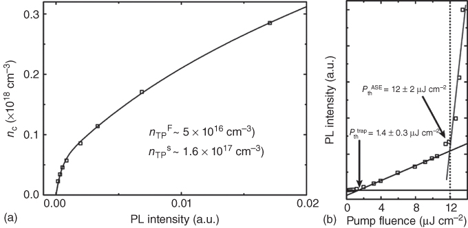
Figure 2.2.3
Determination of the trap state densities. (a) PL intensity as a function of photon‐generated exciton density within the low pump‐fluence range. The experimental data can be well fitted (R
2 = 0.99) with (Eq. 2.2.3) for two types of trapping states. (b) PL intensity as a function of pump fluence. The arrows indicate the trap state saturation threshold fluence ( ) and the ASE threshold fluence (
 ). The dark gray and light gray lines represent the linear fits to experimental data in the two linear regimes of SE and ASE, respectively. The dashed vertical black line indicates the onset of ASE.
Source: Xing et al. 2014 [23]. Copyright 2014. Reprinted with permission of Springer Nature.
Figure 2.2.3a shows a fit of the experimental data over the low pump fluence, which yields two distinct types of traps in MAPbI3 thin films – bulk traps (of trap density ![]() ) with fast trapping times versus surface/interfacial traps (of trap density
) with fast trapping times versus surface/interfacial traps (of trap density ![]() ) with slow trapping times. These elucidated trap densities correlate well with a simple estimate of the total trap density (i.e. bulk and surface) obtained from the intersection of the linearly extrapolated PL intensity with that of the pump‐fluence axis (i.e.
) with slow trapping times. These elucidated trap densities correlate well with a simple estimate of the total trap density (i.e. bulk and surface) obtained from the intersection of the linearly extrapolated PL intensity with that of the pump‐fluence axis (i.e. ![]() – Figure 2.2.3b). This intersection represents the pump fluence needed to fill all the traps (i.e. the threshold trap pump fluence
– Figure 2.2.3b). This intersection represents the pump fluence needed to fill all the traps (i.e. the threshold trap pump fluence ![]() ). Comparatively, the trap densities elucidated here are similar to defect densities in highly ordered organic crystals (1015–1018 cm−3) [24] as well as that of solution‐deposited, high‐temperature‐annealed Cu‐In‐Ga‐S/Se (CIGS) chalcogenide layers (1016 cm−3) [25]; which are better than that of solution‐processed organic thin films (1019 cm−3) [26]. For more details of this approach, the interested reader is directed to the supplementary information of Ref. [23]. The findings of this straightforward approach agree well with another more elaborate kinetic model approach [16] by Stranks et al. (i.e. accounting for exciton formation, exciton dissociation, exciton decay, and free electron trapping) that yielded a trap state density of 2.5 × 1016 cm−3.
). Comparatively, the trap densities elucidated here are similar to defect densities in highly ordered organic crystals (1015–1018 cm−3) [24] as well as that of solution‐deposited, high‐temperature‐annealed Cu‐In‐Ga‐S/Se (CIGS) chalcogenide layers (1016 cm−3) [25]; which are better than that of solution‐processed organic thin films (1019 cm−3) [26]. For more details of this approach, the interested reader is directed to the supplementary information of Ref. [23]. The findings of this straightforward approach agree well with another more elaborate kinetic model approach [16] by Stranks et al. (i.e. accounting for exciton formation, exciton dissociation, exciton decay, and free electron trapping) that yielded a trap state density of 2.5 × 1016 cm−3.
Indeed, first‐principles DFT calculations by Yan's group showed that MAPbI3 possesses unusual defect properties (i.e. p‐type VPb and n‐type MAi being the dominant defect) favorable for solar PV applications [27]. This suggests that MAPbI3 thin film's conductivity can be tuned from intrinsic n‐type to p‐type by adjusting its preparation condition. Their calculations also reveal that defects such as MAi, VPb, MAPb, Ii, VI, and VMA with low formation energies (<0.05 eV) yield shallow levels; while defects such as IPb, IMA, Pbi, and PbI with high formation energies create deep levels. The deep‐level defects are the main source of non‐radiative recombination. Defects with low formation energy may be formed in the mixed perovskite‐based absorbers, or in the interfaces between the perovskite absorbers and contacts. These formation energies strongly suggest that MAPbI3 intrinsically has a rather low non‐radiative recombination rate and is consistent with the long electron–hole diffusion lengths. In view of the high solar cell efficiencies for MAPbI3 thin films, it is unsurprising that the bulk defect densities are low.
2.2.2.4 Transient Spectral Features and Charge Dynamics charge dynamics"?>
Femtosecond transient absorption (TA) spectroscopy is one of the most commonly used techniques to uncover the primary photophysical processes in MAPbI3 perovskites. However, given that the organic component is highly sensitive to external environmental factors (i.e. humidity), sample handling, and fabrication steps, as well as experimental conditions during data acquisition, the observations of TA spectra need to be carefully interpreted.

Figure 2.2.4 Representative linear absorption spectrum (a) of CH3NH3PbI3 or (MAPbI3) showing the absorption edges at ∼480 and ∼760 nm and its TA spectrum (b) showing the PB1, PB2, and PIA signatures at various probe delays. Schematic of PB1 (480 nm) and PB2 (760 nm) contributions from (c) dual valence band model [2] and (d) dual valence band and dual conduction band model [28] and overlapping signals from (e) PbI2 [29] or from (f) iodoplumbate complexes [30].
Source: Sum et al. 2016 [31]. Copyright 2016. Reprinted with permission of American Chemical Society.
Figure 2.2.4 shows the representative linear absorption and TA spectra of CH3NH3PbI3 or (MAPbI3). The latter were obtained with a commercial TA setup (HELIOS, Ultrafast Systems) using a pump of 600 nm and fluence of ∼10 μJ cm−2. There are two distinct negative ΔA valleys located at approximately 480 and 760 nm (simply termed PB1 and PB2, respectively) that originate from a combination of PB (photobleaching) and SE (stimulated emission) signals. A broad positive ΔA (or photoinduced absorption (PIA)) band spans over the 550–650‐nm wavelengths, which is assigned to photoinduced refractive index changes [32]. The two PB signatures agree well with the two absorption edges present in the linear absorption spectrum previously assigned to excitonic transitions. Generally, there is broad agreement over the assignment of the band edge PB2 signal, but the origin of PB1 remains controversial. A detailed model that could account for all these spectral signatures is still lacking. Several interpretations have been proposed: (i) a dual valence band model [2], (ii) a dual conduction band and dual valence band model [28], (iii) overlapping contributions from PbI2 impurities [29], and (iv) charge transfer of iodoplumbate complexes in the fully formed MAPbI3 (or a dual excited state model) [30]. Recent first‐principles band structure calculations have partly supported models (i) and (ii). For Figure 2.2.4c, photoexcitation with energy less than PB1 (i.e. with 600‐nm pulses), the PB1 transition (480‐nm transition) would correspond to the situation where only the CB is populated, hence the dual valence bands. On the other hand, under photoexcitation with energy less than PB1 (i.e. with 510‐ or 580‐nm pulses), as shown in Figure 2.2.4d, the PB1 transition would correspond to situations where only the higher energy valence band (VB2) or the lowest energy conduction band (CB2) are populated, hence the dual conduction bands and dual valence bands. Detailed discussions of the VB/CB assignments in models (i) and (ii) can be found in the supplementary information of Ref. [2] and Chapter of Ref. [28], respectively. Nevertheless, recent detailed TA studies of PbI2 on TiO2 by Flender et al. have shown that the bleaching at 500 nm is unlikely to be related to the plumbate possibly remaining in the perovskite samples, thus discounting model (iv) [33].
Although TA spectroscopy can provide considerable insights into the ground‐ and excited‐state dynamics in MAPbI3 films, it is important not to overgeneralize their findings to the actual performance of perovskite solar cells. The conditions in their device architectures are more complex than in neat films, where the morphology, series and shunt resistances, interfacial traps and band alignments, etc. can have a significant influence on the power conversion efficiency (PCE). There is a complex interplay of these factors in a real device, and these need not be reflected in the TA results of neat or heterojunction films. One should avoid extrapolating and drawing conclusions based on ultrafast optical spectroscopy (UOS) studies alone. UOS studies should be complemented with energetics investigation and materials and device characterization to gain a complete picture (see next section 2.2.3).
2.2.2.5 Photophysical Processes and Their Recombination Constants recombination constants"?>
A common approach to examine the recombination kinetics of thermalized photoexcited free electrons and holes through monomolecular and higher order processes can be described by the following rate equation:
where n is the photoexcited charge carrier density and t is time, k 1 is the monomolecular excitonic‐type recombination or trap‐mediated recombination constant, k 2 is the free carrier bimolecular recombination constant, and k 3 is the three‐body Auger recombination constant. Global fitting the solutions to (Eq. 2.2.4) to the time evolution of the carrier densities at different pump fluences measured by ultrafast spectroscopy techniques (e.g. from TRPL, TA, and time‐resolved THz) such as those shown in Figure 2.2.1 will allow the different rate constants (k 1, k 2, k 3) to be extracted. The rate constants of various perovskite materials are summarized in Table 2.2.1.
Table 2.2.1 List of reported recombination constants for various halide perovskite thin films at room temperature.
| Recombination constants | |||||
| Thin film | k 1 (μs−1) | k 2 × 10⁻¹⁰ (cm3 s−1) | k 3 × 10⁻²⁸ (cm6 s−1) | Techniques | References |
| MAPbI3 | 15 | 0.6 | 1.6 | THz | [34] |
| MAPbI3 | 73 | 1.5 | 3.4 | TA | [35] |
| MAPbI3 | 18 | 1.7 | — | TRPL | [17] |
| MAPbBr3 | 27 | 4.9 | 13.5 | TA | [35] |
| FAPbI3 | 7 | 1.1 | 0.2 | THz | [36] |
| FAPbBr3 | 21 | 11 | 1.5 | THz | [36] |
| MASnI3 | 8 | 14 | — | THz | [37] |
| CsSnI3 | 720 | 100 | — | TRPL | [38] |
MA: methylammonium (CH3NH3 +) and FA: formamidinium (HC(NH2)2 +).
Under low pump fluence excitation (e.g. AM1.5 illumination in solar cells), the photoinduced minority carrier concentration (1015–1016 cm−3) is smaller than the total majority carrier concentration (photoinduced + original doped). The first term in (Eq. 2.2.4) will dominate the second term, and the carrier recombination kinetics is almost monomolecular in nature and exhibits a near monoexponential decay. Strong material dependencies can also be expected for trap‐related recombination channels, because the nature of the traps varies according to film synthesis, processing, and the ensuing morphology. In fact, a wide range of monomolecular charge‐carrier lifetimes (1/k 1) have been reported for MAPbI3, MAPbI3−x Cl x , FAPbI3, thin films, ranging from several nanoseconds to a few microseconds. Much research attention has been directed to the reduction of trap states density (i.e. k 1) in these thin films through optimizing the processing conditions and improving the morphologies.
At higher optical pump fluence, where photogenerated charge‐carrier concentration is much higher than perovskite's trap states density, free electron–hole bimolecular recombination would dominate (i.e. the second term in (Eq. 2.2.4). The charge‐carrier kinetics as a function of pump fluence will follow a power‐law‐type decay. Such bimolecular decay kinetics will continue until the charge‐carrier concentration falls below the trap states density. Upon which, the monomolecular‐type decay will reappear and exhibit as a long exponential tail. In retrospect, the dominant bimolecular nature of the free electron–hole recombination in organic–inorganic lead halide perovskites at excitation fluence of tens of microjoules per square centimeter (or corresponding to carrier densities of ∼1018 cm−3) is now firmly established. This is much larger than the typical PV regime of ∼1013–1015 cm−3. Reported Auger rate constants k 3 vary in the range 0.2–14 × 10−28 cm6 s−1 for various solution‐processed halide perovskite thin films (Table 2.2.1). Auger recombination is unlikely to play a dominant role in PV devices under standard solar illumination, although it may become relevant for the operation of concentrator‐type perovskite PV devices. Nonetheless, Auger effects are still highly relevant in perovskite optical gain media/lasers that operate in the high charge‐density regime.

Figure 2.2.5 A schematic of the photophysical processes and loss mechanisms in perovskites following photoexcitation. Efficient (or strong) pathways and suppressed (or weak) pathways are denoted by the black and gray lines, respectively. Monomolecular recombination is charge carrier density independent, while bimolecular and Auger recombination are charge carrier density‐dependent processes that would typically be present under high‐intensity photoexcitation. In fact, under even higher photoexcitation densities, amplified spontaneous emission (ASE) will out‐compete Auger recombination. However, under solar light intensities (low‐intensity excitation), these latter processes will be strongly suppressed.
Source: Sum et al. 2016 [31]. Copyright 2016. Reprinted with permission of American Chemical Society.
Figure 2.2.5 shows a summative schematic of the key findings in seminal works of the dynamic interplay between the various photophysical processes and relaxation mechanisms in bare solution‐processed MAPbI3 perovskite thin films following photoexcitation [39]. Under low excitation fluence with carrier densities n 0 ≈ 1013−1015 cm−3 (i.e. typical PV conditions), monomolecular processes like trap‐assisted recombination or geminate recombination are found to be inefficient with low first‐order recombination coefficients, k 1 ≈ 10 μs−1 [14]. This observation agrees well with the relatively low trap densities (i.e. n trap 1017 cm−3) [40]. At higher n 0 ≈ 1016−1018 cm−3, multiparticle effects like non‐geminate recombination (bimolecular) and Auger processes (trimolecular) become more important. The non‐geminate recombination arises from the bimolecular recombination of two free charges; which is in contrast to the geminate recombination that originates from the monomolecular annihilation of two Coulombically bound charges. Surprisingly, their bimolecular recombination constants, k 2 ≈ 10−10 cm3 s−1, are approximately four orders lower [10, 14] than Langevin recombination rates for free electron−hole annihilation. However, their Auger rates are found to be large (k 3 ≈ 10−28 cm6 s−1) [14], and in the same order as strongly confined CdSe colloidal quantum dots [41]. Recent works reported that MAPbI3 underwent strong band‐filling effects [5, 15] and bandgap renormalization [32] at higher pump fluence. Depending on the film quality, amplified spontaneous emission (ASE) could even be realized at n 0 ≈ 1018 cm−3, outcompeting the multiparticle processes. More exciting photophysics have also been uncovered recently: correlated electron−hole plasma over the PV and SE fluences [5], the slow hot‐carrier cooling [2] arising from a hot phonon bottleneck effect [32, 42], the microstructure size dependence [43, 44] of the electron–hole interaction and their carrier lifetimes, and the photoinduced refractive index changes [32].
2.2.2.6 Hot Carriers in Perovskites
The previous section mainly discussed the carrier dynamics of thermalized carriers. In contrast, hot carriers refer to those initially generated carriers (i.e. electrons or holes in a Boltzmann distribution) that possess initial kinetic energies at least k BT above the conduction (or valence) bands. The hot‐carrier dynamics in perovskites have been investigated mainly using TA spectroscopy. Since the first report of slow hot‐carrier cooling (∼0.4 ps) in MAPbI3 polycrystalline thin films by Xing et al. in 2013, Li et al. successfully slowed down the cooling by a further 2 orders in MAPbBr3 nanocrystals (up to ∼30 ps) and efficiently (∼83% efficiency) extracted their hot carriers [45]. This later work aptly highlights the potential of perovskites for high‐efficiency hot‐carrier PVs, photocatalysis, and photodetectors. The long hot‐carrier relaxation lifetime and increased hot‐carrier diffusion coefficient are expected to give rise to long hot‐carrier diffusion lengths. By imaging the charge transport using TA microscopy, a hot‐carrier transport as long as ∼600 nm within tens of picoseconds was directly visualized in MAPbI3 thin films [46]. Such long hot‐carrier transport will, in principle, enable hot‐carrier PVs. Presently, the origins of slow hot carrier cooling in halide perovskite thin films are still under intense debate and have been attributed to various contributions such as large polaron screening effect [47], hot phonon effect [42], or acoustical‐optical phonon upconversion [48]. Most recently, Sum's group elucidated a detailed fluence‐dependent picture of the mechanisms of slow hot‐carrier cooling in solution‐processed MAPbI3 thin films [49] using TA spectroscopy and correlating the measurements with detailed theoretical modeling and first‐principles calculations. At moderate carrier concentrations (∼1017–1018 cm−3), carrier cooling is mediated by polar Fröhlich electron–phonon interactions through zone‐center delayed longitudinal optical (LO) phonon emissions (i.e. with a phonon lifetime of ∼0.6 ± 0.1 ps) induced by the hot phonon bottleneck. The hot phonon effect arises from a large energy separation between the LO and longitudinal acoustic (LA) phonon branches, which suppresses the Klemens relaxation pathway essential for LO phonon decay. At high carrier concentrations (∼1019 cm−3), Auger heating further reduces the cooling rates. A clear understanding of these intrinsic photophysics is key to developing disruptive perovskite optoelectronic technologies.
2.2.2.7 Summary and Outlook
CH3NH3PbI3 is now firmly established as the workhorse material in the perovskite field. However, its photophysical properties are highly sensitive to the processing and environmental factors. With the field progressing to newer halide perovskites (e.g. CH3NH3Sn1−x Pb x I3, mixed CH3NH3PbBr3/HC(NH2)2PbI3), and lead‐free systems (e.g. CH3NH3SnI3), there is a greater urgency to thoroughly characterize and establish CH3NH3PbI3 as the model system. One possibility for benchmarking among the various photophysics/photochemistry groups would be to perform round‐robin studies of sealed standard CH3NH3PbI3 (or MAPbI3) films from leading materials laboratories. In the near future, UOS techniques, especially TAS, will continue to play a leading role in probing the photophysical mechanisms and charge dynamics in halide perovskites.
2.2.3 Energetics and Charge Dynamics at Perovskite Interfaces
2.2.3.1 Introduction
Our earlier discussion focused on the intrinsic photophysical properties of bare polycrystalline perovskite thin films. In the absence of any charge extraction heterojunctions, the photoexcited charges in the perovskite film eventually undergo recombination as the system relaxes back to its equilibrium state. In a typical perovskite solar cell, there are two essential interfaces (i.e. perovskite/HTL and perovskite/ETL) sandwiching the halide perovskite active layer to facilitate charge extraction to the electrodes. The presence of these charge transport layers would alter the relaxation pathways seen in the bare perovskite films. Inevitably, the energy‐level alignments at these interfaces would strongly influence the charge‐transfer dynamics. Herein, we examine some of these seminal developments from this perspective in perovskite solar cells.
2.2.3.2 Energetics at the Perovskite/Charge Transport Layer Interfaces charge dynamics!perovskite/charge transport layer interfaces"?>
To facilitate hole transfer, the VBM of perovskite materials must be lower than that of the HTL (e.g. spiro‐OMeTAD); and, conversely, to facilitate electron transfer, the CBM of perovskite materials must be higher than those of ETL (e.g. TiO2 or ZnO). Most papers simply assume that the energy levels of perovskite and the HTL/ETL are aligned from common vacuum levels, assuming that one is dealing with far apart isolated layers. This assumption need not be valid as Fermi‐level pinning could also occur depending on the electronic interaction between the two layers and the position of the band onsets (or gap states) with respect to the vacuum level. Furthermore, interfacial states, interfacial dipoles, and band bending may also be present at the perovskite interface. Such interfacial electronic structures in perovskites would strongly influence the interfacial charge dynamics (e.g. barrier formation affecting the charge transfer); and the features of PV device operation (e.g. photocurrent generation and energy band offsets affecting the open‐circuit voltages).
Photoelectron spectroscopy (PES) provides an important tool to investigate the interfacial energy alignment and electronic structure at material interfaces. The VBM and work function before and after interface formation can be precisely determined. Due to high surface sensitivity of the PES technique, the interface must be carefully prepared (e.g. by thermal deposition and transferred in situ or by spin coating in a glove box, followed by careful transfer in portable transfer capsules to the ultrahigh vacuum (UHV) PES chamber) to avoid external contaminants (such as water vapor and hydrocarbons) from the ambient. The first two PES studies on the energy‐level alignment of perovskite/HTLs are by Schulz et al. [50] and Chen et al. [51]. The former investigated the energy‐level alignments of MAPbI3, MAPbI3−x Cl x , and MAPbBr3 with spiro‐OMeTAD using ultraviolet photoelectron spectroscopy (UPS) and inverse photoelectron spectroscopy (IPES). Their findings revealed a band bending of 0.1–0.3 eV for the spiro‐OMeTAD layer. The latter study investigated the interfacial alignment between MAPbI3 and CuPc (another HTL material) using X‐ray photoelectron spectroscopy (XPS) and UPS, where a 0.3 eV band bending was found for the CuPc layer (Figure 2.2.6b). The band bending observed in these HTLs is a consequence of the Fermi‐level alignment. As the work function of the HTL is smaller than that of the perovskite, charge transfer from the HTL to perovskite occurs as the two Fermi levels align. The reduction of the carriers at the surface of the HTL results in the bending of the bands upward at the interface to higher energies. This could be deleterious for the interfacial charge transfer, resulting in hole trapping and reducing the charge‐transfer efficiency. Therefore, if the work function of the HTL can be slightly increased, the upward band bending (toward the interface) can be suppressed.
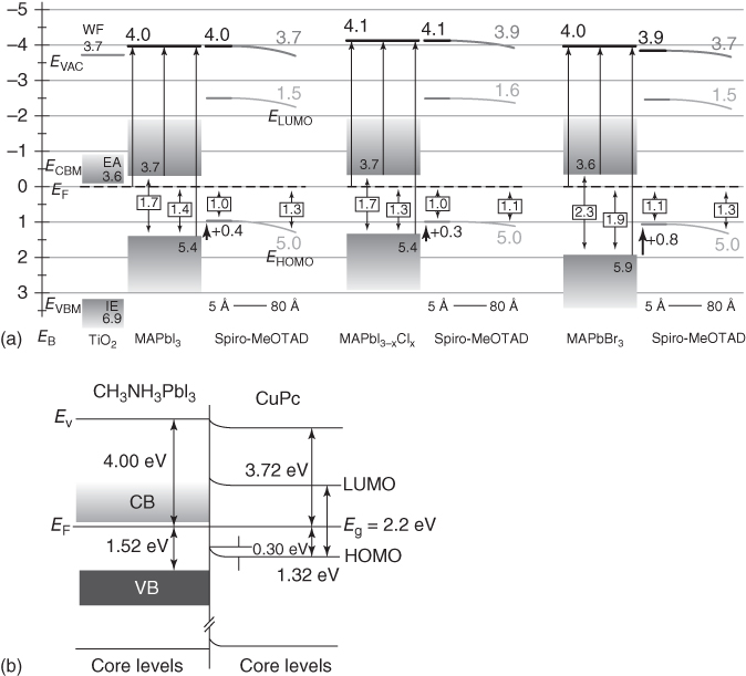
Figure 2.2.6 Energy‐level alignment between perovskite and hole transport materials. (a) MAPbI3, MAPbI3−x Cl x , and MAPbBr3 aligned with spiro‐MeOTAD. (b) MAPbI3 aligned with CuPc where the CuPc energy levels bend down away from the interface. HOMO, highest occupied molecular orbital; LUMO, lowest unoccupied molecular orbital.
Source: (a) Schulz et al. 2014 [50]. Copyright 2014. Reprinted with permission of Royal Society of Chemistry. (b) Chen et al. 2014 [51]. Copyright 2014. Reprinted with permission of American Physical Society.
Conventional PES studies (with Al Kα ∼ 1.486 keV photons) on the perovskite/ETL interface face inherent challenges from the sample preparation. For example, one would not be able to probe the interface of spin‐coated perovskite on the TiO2. To overcome this limitation, Lindblad et al. [52] utilized hard X‐ray PES (with 4 keV photons) that yielded photoelectrons with a much longer inelastic mean free path to probe MAPbI3 spin coated on mesoporous (me)‐TiO2 layers. They found the VBM of MAPbI3 to be 2.1 eV higher than that of TiO2. Based on the values of the optical band gaps for TiO2 (3.2 eV) and MAPbI3 (1.5 eV), they also deduced the CBM of MAPbI3 to be ∼0.4 eV higher than that of TiO2. While this approach increased the sensitivity of the bulk energy levels of perovskite and TiO2 and permits direct referencing between the bulk TiO2 and perovskite, it is still not a direct probe of the interfacial energy alignment. A straightforward approach to study this interface with conventional PES would be to utilize in situ vapor deposition of perovskite materials on TiO2 substrates.
The significance of investigating the interface band alignment is aptly highlighted in several works that reported strong dependence of perovskite's Fermi‐level position on the underlying substrate [53, 54]. The substrate‐type modulates the Fermi energy to VBM difference (E F − E VBM), thereby making the MAPbI3 layer more n‐ or p‐type. Typically, the VBM of MAPbI3 is lowered to ∼1.7 eV on n‐type substrates such as ZnO, TiO2, ZrO2; while it can be significantly lowered to ∼1.38 eV on PEDOT:PSS (poly(3,4‐ethylenedioxythiophene) polystyrene sulfonate); ∼1.0 eV on NiO x and ∼0.9 eV on Cu2O [53]. Such tunability of the Fermi‐level position and the majority carrier type with the substrate is believed to arise from the low density of intrinsic carriers (i.e. from unintentional dopants) and the low density of electronically active mid‐gap bulk and interface defects (or otherwise E F would be pinned) [54]. For future studies, it is extremely important to correlate these findings with interfacial charge‐transfer studies and device characterization to fully understand the extent of the tunability to improve the performance of alternate inverted [55] or tandem [56] perovskite architectures.
2.2.3.3 Charge‐Transfer Dynamics charge dynamics!electron transfer process"?> at the Perovskite/Charge‐Transport Layer Interface
Using infrared TA spectroscopy and microwave photoconductivity, Moser in collaboration with Grätzel and coworkers performed the first study to probe the charge‐transfer mechanism in perovskite solar cells (Figure 2.2.7). They found clear evidence of not only efficient hole injection from photoexcited CH3NH3PbI3 into the HTL (spiro‐OMeTAD) but also efficient electron injection from photoexcited MAPbI3 into the ETL TiO2; both processes occurring simultaneously over comparable ultrafast timescales within 3 ps [57]. Probing at 1.4 μm allowed the authors to directly observe the carrier's population decay within the perovskite itself (Figure 2.2.7b). Using TA spectroscopy, they demonstrated that the population of long‐lived charges in TiO2/MAPbI3/HTM (hole transporting material) samples is higher than that in Al2O3/MAPbI3/HTM samples (Figure 2.2.7b), which in turn indicated a more efficient charge separation in the former than in the later. It was revealed that the efficiency of charge extraction in a perovskite solar cell also depends on the ratio between charge recombination and charge separation rates. In this regard, Moser et al.'s findings showed that it is advantageous to use TiO2 as the electron acceptor and transporter, together with an HTM in perovskite solar cells.
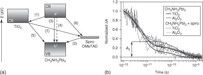
Figure 2.2.7 (a) Schematic diagram of energy levels and electron transfer processes in an HTM/perovskite/TiO2 cell. (1) Electron injection; (2) hole injection; (3) radiative exciton recombination; (4) non‐radiative exciton recombination; (5) back electron transfer at the TiO2 surface; (6) back charge transfer at the HTM surface; (7) charge recombination at the TiO2/HTM interface. (b) Transient absorption signals were measured at a probe wavelength of 1.4 μm following the femtosecond laser‐pulsed excitation at 580 nm: CH3NH3PbI3 (or MAPbI3) on TiO2 (black); CH3NH3PbI3 on Al2O3 (dark gray – lower trace); CH3NH3PbI3 and spiro‐OMeTAD on TiO2 (dark gray – upper trace); CH3NH3PbI3 and spiro‐OMeTAD on Al2O3 (light gray). Thick solid lines represent bi‐exponential fits of experimental points starting at time t = 1 ps. A 2 represents the normalized absorbance change at 25 ps, used as a metric to compare the various samples.
Source: Marchioro et al. 2014 [57]. Copyright 2014. Reprinted with permission of Springer Nature.
Although TiO2 is the workhorse electron acceptor in perovskite PVs, a detailed understanding of the interfacial charge‐transfer mechanisms at this heterojunction remains incomplete. In particular, there have been diverse conclusions about the charge‐transfer times (i.e. spanning <1 ps to hundreds of picoseconds) and charge‐transfer efficiencies have been obtained for the MAPbX3/TiO2 heterojunction (see summary in Table 2.2.2). The confusion could be partly traced to the mesoporous TiO2 as the nanopores can greatly alter the perovskite's film morphology and crystallinity. Hence, systematic studies of the interfacial charge‐transfer dynamics and comparison with other standard samples (e.g. perovskite/quartz, perovskite/Al2O3) are particularly difficult to achieve. Nevertheless, these diverse observations of the charge‐transfer times together with evidence of carrier accumulation [63] in MAPbI3 and anomalous I–V hysteresis observed in MAPbX3/TiO2 heterojunction‐based solar cells [64] indicate that the charge transfer at this interface may be more complex than was previously believed.
Table 2.2.2 List of reported electron transfer times from perovskite to TiO2.
| Type of interface | Techniques | Charge‐transfer time/efficiency | References |
| MAPbI3/me‐TiO2 | TA | ∼3 ps | [57] |
| MAPbI3/planar TiO2 | TA | 39.9 ± 2.5 ps | [29] |
| MAPbI3/me‐TiO2 | TA | 89.6 ± 12.5 ps | |
| MAPbI3/me‐TiO2/planar TiO2 | TA | 150.0 ± 17.6 ps | |
| MAPbI3/me‐TiO2 | TA | 260–307 ps | [58] |
| MAPbI3/me‐TiO2 | TR‐THz | <1 ps | [13] |
| MAPbI3/me‐TiO2 | TA | <200 fs | [59] |
| MA(1−y)FA y PbI x Br(3−x)/me‐TiO2 | TA | ∼100 fs | [60] |
| MAPbI3/TiO2 | DFT calculation | <100 fs | [61] |
| MAPbI3/me‐TiO2/planar TiO2 | TRPL | Quenching efficiency 99% | [13] |
| MAPbI3/planar TiO2 | PL | Quenching efficiency 47% | [62] |
Through TRPL and TA spectroscopy, Xing et al. found that the electron transfer at the MAPbI3/compact TiO2 interface to be slower than that at the MAPbI3/PCBM ([6,6]‐phenyl‐C‐61‐butyric acid methyl ester) interface [65]. These findings concur with those of Wojciechowski et al., who had also observed slow electron transfer at the MAPbI3−x Cl x /TiO2 interface, in contrast to the effective quenching at the MAPbI3−x Cl x /PCBM or C60‐SAM (self‐assembled monolayer) interfaces [66]. From the deficiency of surface organic cations (i.e. electron deficiency) in MAPbI3 elucidated from XPS studies, Xing et al. deduced that the passivation of the surface states of MAPbI3 and TiO2 resulted in the formation of a strong interfacial dipole, which would function as an electron barrier at the MAPbI3/TiO2 interface. Consequently, this leads to PL intensity enhancement and PL lifetime lengthening for MAPbI3 interfaced to compact TiO2. This work aptly highlights the significance of complementary energetics and charge dynamics approach to tackle material interface problems. The presence of this interface is consistent with the observations of carrier accumulation [63] in MAPbI3 from impendence spectroscopy and could possibly be one of the contributions to the anomalous I–V hysteresis observed in MAPbX3/TiO2 heterojunction‐based solar cells [64]. More recently, Nazeeruddin and coauthors reported an ultrafast interfacial electron injection from mixed‐halide iodide−bromide perovskite MA1−y FA y PbI x Br3−x into mesoporous TiO2 within ∼100 fs [60]. Such rapid electron transfer competes successfully with the electron–phonon energy relaxation inside the perovskite, demonstrating that hot charge carriers can be harvested before they thermalize, a potential way to break the Shockley–Queisser limit and boost the device efficiency. Further energetics and charge dynamics studies on other perovskite/ETL interfaces (e.g. MAPbX3/ZnO) can be expected.
2.2.3.4 Summary and Outlook
Moving forward, it is important that charge dynamics studies at the perovskite/inorganic semiconductor interface should be accompanied by both energetics and physical studies to understand the intrinsic chemical and morphological nature of the surface where various defect types (e.g. surface traps, vacancies, etc.) and crystal sizes are inevitably present. The perovskite sample fabrication (i.e. single‐step deposition, dual‐deposition processing, and evaporation approach), processing (i.e. annealing temperatures and duration), and ambient conditions (i.e. the oxygen and moisture content in the glove box) all exert a profound influence on the perovskite film quality and its morphology and surface properties. Hence, the inclusion of XPS data of the perovskite surface in dynamics studies could help diagnose the surface chemical nature of the perovskite films made by various research groups, thereby permitting better comparison. Such standardization will become more important as surface engineering approaches are now becoming increasingly popular. Apart from energetics studies, careful control of the pump fluence in the dynamics studies is also important as the use of relatively high pump fluence would mask the effects of carrier accumulation (if a barrier is present) with a flood of photoexcited carriers. Similarly, use of pump energies far larger than the perovskite bandgap will generate a population of hot carriers that could overcome the barrier with hot‐carrier transfer [65]. Any of these factors or a combination of them are likely to influence the interfacial charge‐transfer times listed in Table 2.2.2, thus causing the spread. Further studies are needed to clarify this.
2.2.4 Toward Perovskite Single‐Crystal Photovoltaics
Large‐scale SCs typically possess fewer defects compared to polycrystalline or amorphous thin films. Hence, organic–inorganic halide perovskite SCs are expected to yield even better PV performances. Theoretical calculations have shown that efficiencies up to 25% can be obtained for large crystals (i.e. diameter > 10 μm), which is higher than those with smaller grain sizes [67]. A breakthrough in synthesizing large perovskite SCs using solution methods in 2015 has thrown them into the spotlight [22, 68–71]. Based on the historical developments for Si and GaAs solar cells, one can expect that perovskite PVs would soon embark on the same path toward single‐crystalline solar cells. In this section, we focus on the photophysics of organic–inorganic halide perovskite SCs.
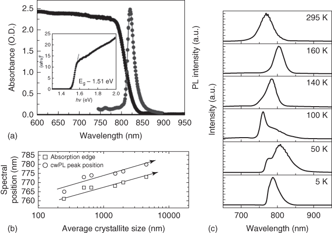
Figure 2.2.8 Absorption and PL properties of MAPbI3 SCs. (a) Absorption and PL profile of a MAPbI3 SC. (b) Grain‐size‐dependent PL energy shift. (c) Temperature‐dependent MAPbI3 SC PL profile change.
Source: (a) Saidaminov et al. 2015 [70]. Copyright 2015. Reprinted with permission of Nature Publishing Group. (b) D'Innocenzo et al. 2014 [72]. Copyright 2014. Reprinted with permission of American Chemical Society. (c) Fang et al. 2015 [73]. Copyright 2015. Reprinted with permission of John Wiley & Sons.
2.2.4.1 Absorption and Emission Properties emission properties"?>
Unlike perovskite polycrystalline thin films, the absorption edge of perovskite SCs is usually extended. Figure 2.2.8a shows the typical absorption and emission profiles of MAPbI3 SC, where its absorption edge is redshifted by around 0.1 eV (∼50 nm) compared to the polycrystalline thin films (as shown in Figure 2.2.1) [22, 70]. The extended absorption, exhibiting a shoulder centered at around 800 nm, also contributes to the external quantum efficiency (EQE) of MAPbI3 SC‐based solar cells [22]. The extended absorption is possibly due to the weak absorption from the Urbach tail that only becomes pronounced in thick crystals. We note that this energy shift is also seen in the emission spectra. Using two‐photon excitation, the bulk regions of the SC can be excited. Yamada et al. found the PL peak of MAPbI3 crystal to be around 812 nm, which is redshifted compared to polycrystalline thin films (∼770–780 nm). One possibility for the emission redshift could be due to reabsorption [74]. As photons emitted in the interior pass through the thick crystal to the collection optics, the blue side of the spectrum becomes absorbed by the crystal. Such phenomenon usually happens in crystals with large band‐to‐band absorption and small Stokes shift [74]. The reabsorption will reshape the PL spectra, resulting in the redshift and narrowing of the spectrum. Another possibility for the emission redshift is that the bandgap energies of the MAPbI3 polycrystalline thin film and SC are different. The difference could arise from the size effect. For example, MAPbI3 perovskite in mesoporous TiO2 matrix is found to have blueshifted absorption and PL spectra compared to polycrystalline thin films with relatively larger crystalline size [75]. As grain size decreases, the absorption edge and PL is found to continuously blueshift, while the linewidth is also simultaneously broadened (Figure 2.2.8b) [68, 72]. Smaller crystals may suffer from stronger inorganic cage deformation that compresses the lattice, resulting in an increased bandgap [68, 76]. These bandgap changes suggest a means of tuning the perovskite emission and broadening the light‐harvesting spectrum by simply varying the crystal size [72].
Apart from tuning the bandgap, varying the crystal size also affects the nature of the primary photoexcited species – excitons versus free carriers (discussed earlier). The electron–hole interaction in hybrid perovskite system is sensitive to the microstructure of the material. Larger MAPbI3 SCs show an excitonic transition at the absorption edge, which is absent in small crystals. It is speculated that the formation of excitonic transition in large crystals is related to the ordering of the system, particularly the orientational order of the organic cation (methylammonium, MA +). The organic cation has a permanent dipole. If it can freely rotate, separation of electron–hole pairs is facilitated due to the increase of the low‐frequency dielectric constant. However, in SCs, the rotational disorder of the cations is quenched. Thus, free carriers will thermalize and coalesce into forming excitons [43].
The emission spectra become more complicated at low temperatures when phase transitions occur (Figure 2.2.8c) [73]. Above the phase transition temperature (163 K for MAPbI3), the PL spectrum shifts from 770 to 805 nm when the temperature drops, corresponding well with the absorption edge redshift and is attributed to the band‐edge transition. Between 163 and 125 K, a blueshift of the PL peak occurs – opposite to the shift above 163 K. Below 100 K, a new band appears at ∼805 nm and gradually dominates with lowering temperatures. Below the phase transition temperature, the PL spectra can be fitted using three Gaussian peaks. The high‐energy peak (I) is assigned to free exciton (FE) emission, while the intermediate (II) and low (III) energy peaks are attributed to bound excitons (BEs). The BEs have long lifetimes and strong emission, possibly attributed to the localization caused by site distribution of the organic cations at low temperatures. For MAPbBr3 SCs, hydrogen‐like Wannier–Mott exciton emission was also observed. The first and second exciton transitions were found at 2.2558 and 2.2673 eV. According to the relation of the band‐edge (E g) and exciton binding energy (E b): E n = E g − E b/n 2, where n = 1, 2, 3, …; an exciton binding energy of 15.9 meV was derived. Donor–acceptor (D–A) pair emission dictates the sub‐bandgap emission band at low temperature [77]. With increasing excitation power, the D–A band does not increase in intensity, but instead shows a pronounced blueshift, corresponding to the increase of recombination events for close‐by electron–hole pairs.
2.2.4.2 Surface Versus Bulk Optical Properties
In large semiconducting crystals, the surface and the bulk properties are usually distinct from each other. Surface defects and imperfections such as dangling bonds, dislocations, and chemical impurities adsorbed can result in very different optical and electronic properties at the surface compared to the bulk part. For example, moisture can cause a significant blueshift of MAPbI3 SC emission from 796 to 770 nm [78]. Such a change is related to the surface‐hydration‐induced lattice expansion, which results in local stress and the surface reconstruction [79]. Distinct PL blueshift from the bulk to the surface was also observed when using one photon to excite the surface and two‐photon excitation for the bulk [80]. However, reabsorption effects cannot be neglected here due to much deeper penetration depth with two‐photon excitation. To further understand the surface defect properties and their effects, photocarrier dynamics with different surface passivation were also investigated. The passivation with an electron‐rich ligand (hexylthiophene) was found to significantly improve MAPbI3 SC emission intensity and carrier lifetime, while it also helps reduce the BE formation at low temperature. This implies that the electron‐rich sulfur of the hexylthiophene donates its electrons to positively charged defects (likely to be iodide vacancies) at the surface of MAPbI3 crystals.
Surface recombination occurring at the free surface or grain boundaries can also be a dominating factor limiting the device efficiency. This can result in a fast initial decay of the carrier density. For large crystals, their surfaces usually have much higher defect densities than those of the bulk in SC, thereby resulting in high surface recombination rates. The minority carrier lifetime can be expressed as
where 1/τ surface, 1/τ radiative, 1/τ defect are the surface, radiative, and bulk Shockley–Read–Hall (SRH) recombination rates, respectively; and higher order recombination is excluded in the expression. An important parameter to quantify the quality of a surface is the surface recombination velocity (SRV), which is defined by the ratio of the recombination rate per unit area (U s) to the excess carrier concentration close to the surface (Δn):
Due to the presence of the surface recombination, the carrier dynamics of perovskite SC usually exhibits a bi‐exponential decay manner. The initial fast decay with a lifetime of ∼ns is attributed to the surface recombination, while the longer component is attributed to the bulk recombination lifetime [69, 81]. Quantification of the SRV is usually through TA spectroscopy or TRPL spectroscopy. For example, in MAPbBr3 SCs, the SRV is around 3.4 × 103 cm s−1 (TA spectroscopy) and ∼6.7 × 103 cm s−1 (TRPL), while that for MAPbI3 SCs is about half of the MAPbBr3 values [80]. SRV as low as a few centimeters per second had been reported for MAPbBr3 SC [82]. Surprisingly, the SRV of polycrystalline MAPbI3 thin films (0.45 × 103 cm s−1) was found to be more than six times lower than in the SCs (0.45 × 103 cm s−1), possibly due to excess MA cations that passivate grain boundaries in the former. For SCs, a Pb2+‐rich environment was found instead [83]. We have to point out that in SCs or in polycrystalline thin films, the SRVs are generally a few orders lower than conventional non‐passivated PV semiconductors such as GaAs, CdTe (105–106 cm s−1). Considering that surface recombination occurs in an SRH‐like trend, recombination via mid‐gap traps created by surface defects will dominate and influence the SRV. In organic–inorganic halide perovskites, the defects at the grain boundaries or surfaces give rise to very few mid‐gap states for recombination [84]. An empirical criterion to estimate the magnitude of SRV in semiconductors is to compare the position of the semiconductor band energy with the Fermi‐level stabilization energy [85]. The Fermi‐level stabilization energy (E FS), also known as the neutral level, located at around 4.9 eV below the vacuum level, is the reference energy used to predict the dominant semiconductor native defects. For GaAs and CdTe, that E FS lies near the middle of their bandgap, the SRVs are much higher (>105 cm s−1), and therefore surface passivation is usually necessary [86]. For semiconductors such as InP as well as halide perovskites (MAPbI3, MAPbBr3), the E FS lies either near the CBM or VBM, indicating that the native defects tend to form away from the mid‐gap, and hence provide small SRV for MAPbI3 (∼103 cm s−1) and InP (∼102 cm s−1) SCs [80, 87]. The SRV is so low in perovskite SCs that it indicates that surface passivation is unnecessary for optimizing the PV performance when grain sizes are larger than ∼30 μm [81].
2.2.4.3 Carrier Lifetimes, Diffusion Lengths, and Diffusion Coefficients
With regards to PV application, apart from the earlier discussion, other key parameters include carrier lifetime τ (surface and bulk carrier lifetime), mobility μ, diffusion length L D, and trap density n t [69].
τ can be determined from the decay transients from TA spectroscopy or TRPL spectroscopy. For example, the dynamics of MAPbX3 SCs usually show a bi‐exponential decay [68, 69, 81]. A shorter decay time constant can be attributed to the lifetime at the surface part of the SC where surface recombination dominates. The longer component is due to the bulk carrier lifetime [81]. As shown in Figure 2.2.9a, the MAPbI3 SC's surface carrier lifetime was measured to be ∼18 ns, while the bulk lifetime was 570 ns – obtained using TA spectroscopy [70]. With other techniques, such as impedance spectroscopy and transient photovoltage measurements, the bulk carrier lifetime in MAPbI3 SC is found to be as high as 82–95 μs [22].
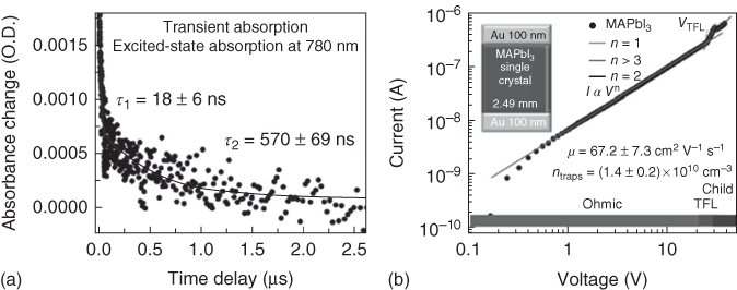
Figure 2.2.9 (a) Trap density of MAPbI3 SC measured using trap‐filled limit voltage. (b) Carrier lifetime measured using time‐resolved PL spectroscopy.
Source: Saidaminov et al. 2015 [70]. Copyright 2015. Reprinted with permission of Nature Publishing Group.
μ is usually measured using space‐charge‐limited‐current (SCLC), time‐of‐flight (ToF), Hall measurements, etc. High carrier mobilities were found for solution‐processed MAPbX3 SCs. For example, Dong et al. reported a hole mobility of 164 ± 25 cm2 V−1 s−1 and electron mobility of 24.8 ± 4.1 cm2 V−1 s−1 for MAPbI3 using the SCLC and ToF techniques [22]. For MAPbBr3, high carrier mobility of 115 cm2 V−1 s−1 was also reported by Shi et al. using ToF measurements [69]. For MAPbCl3, the carrier mobility is 42 ± 9 cm2 V−1 s−1 from SCLC measurements [71]. The carrier mobilities obtained for SCs are generally 1–2 orders higher than those for polycrystalline thin films.
L D can be estimated from the expression:
where τ is the carrier lifetime and D is the diffusion coefficient that can be expressed using the following Einstein relation: D=μV t , where μ is carrier mobility, V t is the thermal energy. The diffusion length of MAPbI3 SC is frequently reported to range from a few micrometers to hundreds of micrometers [22, 69]. Such a high carrier diffusion length implies that a perovskite SC‐based PV device would be able to absorb all the above bandgap light and extract all the carriers generated simultaneously. The high carrier mobility and diffusion length is a result of the greatly reduced defect density in the bulk SC compared to the polycrystalline. As shown in Figure 2.2.9b, trap density estimated for MAPbI3 SCs is on the order of 1010 cm−3 using trap‐filled limit voltage (V TFL), which is 5 orders lower than that of polycrystalline perovskite thin films measured using the same technique [22, 69].
2.2.4.4 Transient Spectral Features and Excitation Dynamics excitation dynamics"?>
The ability to interpret and discern the transient spectral features and excitation dynamics in perovskite SCs is key to understanding its full photophysics picture. A particularly problematic dilemma in the characterization of the large and thick perovskite SCs (several millimeters) is the limited penetration depth (of several 100 nm) for above bandgap photons via single‐photon excitation. Two‐photon excitation offers a viable solution. For example, it was reported that MAPbBr3 SCs have two‐photon absorption (TPA) coefficients of ∼8.6 cm GW−1 at 800 nm excitation [88], which can result in a penetration depth of around 100 μm. Recently, Wu et al. utilized a combination of one‐photon and two‐photon excitation spectroscopy to elucidate a comprehensive photophysical picture of the surface and bulk regions of perovskite SCs.

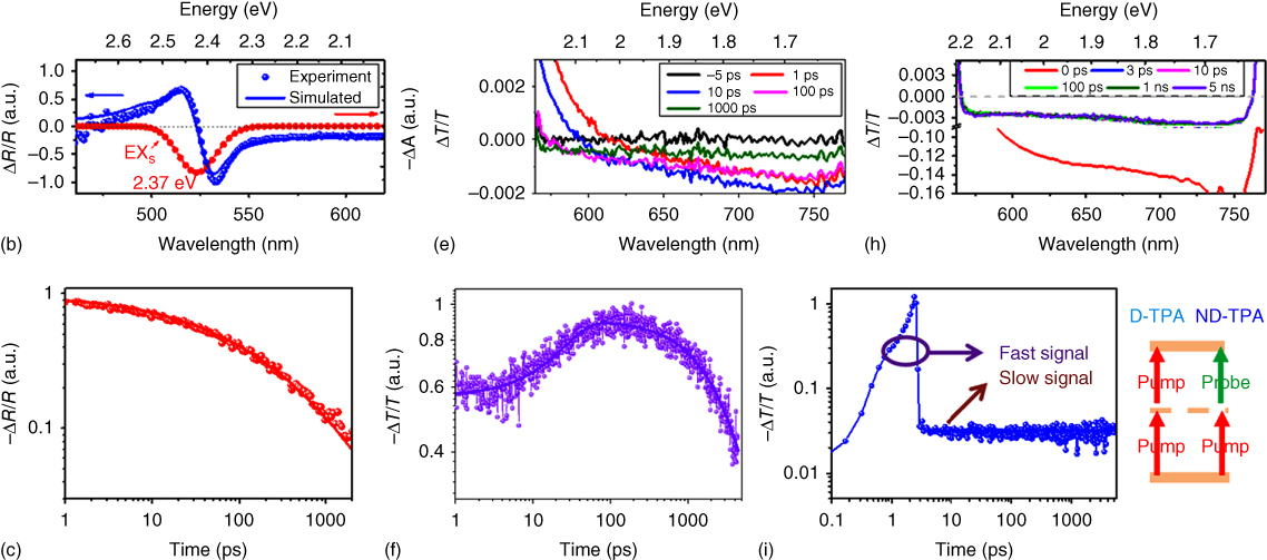
Figure 2.2.10 Femtoseconds to nanoseconds transient absorption of MAPbBr3 single crystal. (a) The pseudocolor transient reflectivity (TR) profile of MAPbBr3 with 400 nm excitation. (b) The TR profile (experimental result selected at 10 ps delay) (blue dot) and the fitted curve (blue solid) using surface exciton absorption (red line). (c) Normalized TR dynamics monitored at 532 nm and the fitted curves using model depicted in the text. (d) The pseudocolor transient absorption (TA) profile of MAPbBr3 with 400 nm excitation. (e) TA profile of MAPbBr3 SC at selected delays excited by 400 nm. (f) Normalized transient dynamics monitored at 700 nm for MAPbBr3 SC with 400 nm excitation. (g) The pseudocolor TA profile of MAPbBr3 with 800 nm excitation. Inset shows the zoom‐in profile near time zero. (h) TA profile of MAPbBr3 SC at selected delays excited by 800 nm. (i) Normalized transient dynamics monitored at 700 nm for MAPbBr3 SC with 800 nm excitation. (The time zero has been shifted for better display.) The right side shows a schematic of the D‐TPA and ND‐TPA.
Source: Wu et al. 2016 [80]. Copyright 2016. Reprinted with permission of John Wiley & Sons.
Figure 2.2.10a shows the pseudo‐color transient reflectivity (TR) spectra feature of a MAPbBr3 SC with 400 nm excitation. Two anti‐symmetric peaks were found centered around 2.3–2.4 eV (Figure 2.2.10b) [80, 81]. The shape of the TR spectra is consistent, except for the drop in magnitude with time. As organic–inorganic halide perovskites possess a large refractive index (n ∼ 2–3), the TR is dominated by the refractive index change [32]:
where n(E) and Δn(E) are the steady‐state reflective index and reflective index change after excitation at photon energy E. The change of the refractive index is associated with a change of absorption coefficient Δα, through the Kramers–Kronig relations:
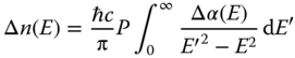
where c is the speed of light and P is the Cauchy principal integral.
Upon photoexcitation, the excitonic absorption peak and/or continuum bands are filled, leading to an absorption bleach at the probe wavelengths (Δα < 0). Under low‐fluence photoexcitation, the bleaching of the continuum band is negligible due to the low occupation probability. As shown in Figure 2.2.10b, the TR profile of MAPbBr3 can be well fitted with an excitonic bleach at around 2.37 eV, confirming the validity of this interpretation. Due to the abrupt change in refractive index at the air/perovskite interface, the TR profile and dynamics are mainly from the very shallow surface region (∼10 nm) [89]. With 400‐nm excitation, the TR dynamics shown in Figure 2.2.10c originates from surface recombination dynamics and diffusion into the bulk. Hence, excitation wavelengths with different absorbing lengths will yield strikingly different TR dynamics due to the two varying contributions from surface recombination and diffusion [81].
On the other hand, if pump‐probe spectroscopy is performed in transmission mode, no TA signal can be detected below 560 nm (2.22 eV) due to the strong absorption of the transmitted probe by the thick MAPbBr3 SC (Figure 2.2.10d). The TA spectra show a negative change in transmission (ΔT < 0) at wavelengths >620 nm. Also evident is an isosbestic point (occurring around 620 nm at 1 ps) that gradually blueshifts at longer delays, separating the −ΔT in the redder part of the spectrum from the +ΔT (or PB) in the bluer part. This +ΔT region is from the tail of the PB peak (arising from state‐filling and SE following absorption of the pump beam). However, the PIA region (−ΔT) that is present in SCs is absent in the TA spectrum of the polycrystalline thin film, indicating that it is a unique spectral feature of SCs. The PIA possibly arises from the transitions of the photoexcited species to higher excited states or sub‐bandgap trap state absorption in the crystal, which is significant in thick crystals while being negligible in thin films. The fast blueshift of the isosbestic point and the disappearance of the PB band within 100 ps (Figure 2.2.10e) indicate that the excited species at the surface diffuses very efficiently into the bulk. The build‐up time (∼100 ps) of the PIA yields a diffusion length of 48 nm using the diffusion equation of ![]() . This value represents the average propagation distance of the excited species away from the surface photoexcited region into the bulk. The fitted PIA decay lifetime of ∼3.8 ns (Figure 2.2.10f) is in between the value of the PL lifetimes of the true surface (∼1 ns) and true bulk (∼34 ns) values, constituting an average lifetime [80].
. This value represents the average propagation distance of the excited species away from the surface photoexcited region into the bulk. The fitted PIA decay lifetime of ∼3.8 ns (Figure 2.2.10f) is in between the value of the PL lifetimes of the true surface (∼1 ns) and true bulk (∼34 ns) values, constituting an average lifetime [80].
Figure 2.2.10g shows a pseudo‐color TA profile of the SC with two‐photon pumped (800 nm) excitation. In the first few picoseconds timescale, an ultrafast and strong PIA component appears immediately after excitation spanning the wavelength range of ∼650−750 nm (Figure 2.2.10h). After the decay of this “ultrafast” component, a residue PIA component (slow) similar to that observed in 1PA excitation at long delays persists and does not show any decay within the 5 ns time window (Figure 2.2.10i). The ultrafast PIA component is an artifact that originates from the nondegenerate (ND)‐2PA of the pump and probe – i.e. simultaneous absorption of a pump and a probe photon resulting in a TPA process. The “slow” component, on the other hand, is the “real” carrier relaxation dynamics following photoexcitation by degenerate (D)‐2PA of the pump photons (Figure 2.2.10i schematic). The constant nonequilibrium ΔT/T signal over the 5 ns time window suggests the presence of a long‐lived species in the bulk – in fact, its lifetime corresponds well with the bulk emission lifetime (30–40 ns) and is attributed to the bulk excitation recombination [80].
Table 2.2.3 List of reported recombination constants for various halide perovskite single crystals at room temperature.
| Recombination constants | ||||
| Thin film | k 1 (μs−1) | k 2 × 10⁻¹⁰ (cm3 s−1) | Techniques | References |
| MAPbBr3 | 40 | 5.4 | TRPL | [90] |
| FAPbBr3 | 15 | 3.5 | TRPL | [90] |
| CsPbBr3 | 21 | 5.7 | TRPL | [90] |
| MAPbBr3 | 29 | 2.0 | TRPL | [80] |
| MAPbI3 | 0.7–0.8 | 0.38–0.82 | (Micro‐)TRPL | [91] |
| MAPbBr3 | 2.5 | 2.0 | (Micro‐)TRPL | [91] |
MA: methylammonium (CH3NH3 +) and FA: formamidinium (HC(NH2)2 +).
2.2.4.5 Recombination Constants in the Surface and Bulk Regions bulk regions"?> of Perovskite Single Crystals
Table 2.2.3 lists the recombination constants of several typical perovskite SCs. The monomolecular recombination coefficient (k 1) of SCs has been widely reported, corresponding to the inversion of the carrier lifetime under low fluence, as discussed. The SCs generally have a lower k 1 rate due to the presence of much lower trap density than do polycrystalline films. For example, the observed k 1 for MAPbI3 SC is usually around 0.1–10 μs−1, which is much lower compared to MAPbI3 polycrystalline thin films with typical lifetimes of nanoseconds to microseconds (corresponding to a k 1 of 1–103 μs−1). Under high excitation densities, processes such as bimolecular and Auger recombination at the surface and bulk regions, as well as carrier diffusion would contribute to the observed decay dynamics and complicate the analysis. Hence, there have been few reports on the bimolecular and Auger recombination coefficients (k 2 and k 3). As Table 2.2.3 shows, the bimolecular recombination coefficients of lead bromide SCs are generally accepted on the order of 10−10 cm3 s−1, similar to that of polycrystalline thin films. Lead iodide SCs have a coefficient of around 10−11 cm3 s−1, which is slightly lower than polycrystalline thin films. Presently, there has been no report on the Auger recombination coefficients for SCs, which warrants further investigations.
Perovskite SCs are expected to have high potential application as PV materials. They possess many improved optoelectronic properties compared to their polycrystalline counterparts, such as much reduced trap density, lengthened carrier lifetime, improved diffusion length, reduced bandgap, etc. However, unlike polycrystalline thin films, perovskite SCs are relatively unexplored. For example, the bulk regions of the SCs still remain poorly understood compared to the surface part in spectroscopic characterization due to the limited above bandgap light penetration depth (∼102 nm). For example, photophysics properties such as exciton binding energy, PL quantum yield, bimolecular/Auger recombination coefficients, and hot‐carrier relaxation are still unknown in the bulk. These bulk properties are very important, as they provide us an excellent platform to correlate with theoretical simulation and understand the intriguing fundamental properties. Meanwhile, developing a practical approach to synthesize thin SC films (e.g. ∼1 μm thickness) should be the focus to boost the perovskite solar efficiency up to 25%.
2.2.5 Concluding Remarks
The rapid ascent of organic‐inorganic lead halide perovskite to the world stage has presented both opportunities and challenges for the PV and materials characterization communities. With single‐junction polycrystalline perovskite solar cells inching toward their Shockley–Queisser limits, one can look forward to the development of newer architectures like tandem and hot‐carrier perovskite solar cells (or a combination of both) to breach that limit. Given the much better properties of perovskite SCs compared to their polycrystalline counterparts, one could also envisage new developments in that direction. However, a key challenge is to be able to grow large area and continuous SC thin films. Nonetheless, nondestructive and noncontact spectroscopy techniques will continue to play a vital role in understanding the photophysical properties, interfacial energetics, and charge‐transfer mechanisms in these next‐generation perovskite solar cells.
References
- 1 Even, J., Pedesseau, L., and Katan, C. (2014). J. Phys. Chem. C 118: 11566.
- 2 Xing, G.C., Mathews, N., Sun, S.Y. et al. (2013). Science 342: 344.
- 3 Even, J., Pedesseau, L., Katan, C. et al. (2015). J. Phys. Chem. C 119: 10161.
- 4 D'Innocenzo, V., Grancini, G., Alcocer, M.J.P. et al. (2014). Nat. Commun. 5: 3586.
- 5 Saba, M., Cadelano, M., Marongiu, D. et al. (2014). Nat. Commun. 5: 5049.
- 6 Sum, T.C., Chen, S., Xing, G.C. et al. (2015). Nanotechnology 26: 342001.
- 7 Koutselas, I.B., Ducasse, L., and Papavassiliou, G.C. (1996). J. Phys. Condens. Matter 8: 5953.
- 8 Hirasawa, M., Ishihara, T., Goto, T. et al. (1994). Physica B 201: 427.
- 9 Ishihara, T. (1994). J. Lumin. 60–61: 269.
- 10 Savenije, T.J., Ponseca, C.S., Kunneman, L. et al. (2014). J. Phys. Chem. Lett. 5: 2189.
- 11 Ip, K.M., Wang, C.R., Li, Q., and Hark, S.K. (2004). Appl. Phys. Lett. 84: 795.
- 12 Sheng, C.X., Zhang, C., Zhai, Y.X. et al. (2015). Phys. Rev. Lett. 114: 116601.
- 13 Ponseca, C.S., Savenije, T.J., Abdellah, M. et al. (2014). J. Am. Chem. Soc. 136: 5189.
- 14 Wehrenfennig, C., Eperon, G.E., Johnston, M.B. et al. (2014). Adv. Mater. 26: 1584.
- 15 Manser, J.S. and Kamat, P.V. (2014). Nat. Photonics 8: 737.
- 16 Stranks, S.D., Burlakov, V.M., Leijtens, T. et al. (2014). Phys. Rev. Appl. 2.
- 17 Yamada, Y., Nakamura, T., Endo, M. et al. (2014). J. Am. Chem. Soc. 136: 11610.
- 18 Lee, M.M., Teuscher, J., Miyasaka, T. et al. (2012). Science 338: 643.
- 19 (a) Burschka, J., Pellet, N., Moon, S.J. et al. (2013). Nature 499: 316.(b) Zhou, H.P., Chen, Q., Li, G. et al. (2014). Science 345: 542.
- 20 Stranks, S.D., Eperon, G.E., Grancini, G. et al. (2013). Science 342: 341.
- 21 Docampo, P., Hanusch, F.C., Stranks, S.D. et al. (2014). Adv. Energy Mater. 4.
- 22 Dong, Q.F., Fang, Y.J., Shao, Y.C. et al. (2015). Science 347: 967.
- 23 Xing, G., Mathews, N., Lim, S.S. et al. (2014). Nat. Mater. 13: 476.
- 24 Mehraeen, S., Coropceanu, V., and Bredas, J.L. (2013). Phys. Rev. B 87: 195209.
- 25 Graetzel, M., Janssen, R.A.J., Mitzi, D.B., and Sargent, E.H. (2012). Nature 488: 304.
- 26 Willa, K., Hausermann, R., Mathis, T. et al. (2013). J. Appl. Phys. 113: 133707.
- 27 Yin, W.‐J., Shi, T., and Yan, Y. (2014). Appl. Phys. Lett. 104: 063903.
- 28 Marchioro, A. (2014). Interfacial Charge Transfer Dynamics in SolidState Hybrid Organic‐ Inorganic Solar Cells. Ph.D. Thesis. École polytechnique federale de Lausanne.
- 29 Wang, L.L., McCleese, C., Kovalsky, A. et al. (2014). J. Am. Chem. Soc. 136: 12205.
- 30 Stamplecoskie, K.G., Manser, J.S., and Kamat, P.V. (2015). Energy Environ. Sci. 8: 208.
- 31 Sum, T.C., Mathews, N., Xing, G. et al. (2016). Acc. Chem. Res. 49: 294.
- 32 Price, M.B., Butkus, J., Jellicoe, T.C. et al. (2015). Nat. Commun. 6.
- 33 Flender, O., Klein, J.R., Lenzer, T., and Oum, K. (2015). Phys. Chem. Chem. Phys. 17: 19238.
- 34 Milot, R.L., Eperon, G.E., Snaith, H.J. et al. (2015). Adv. Funct. Mater. 25: 6218.
- 35 Yang, Y., Yang, M.J., Li, Z. et al. (2015). J. Phys. Chem. Lett. 6: 4688.
- 36 Rehman, W., Milot, R.L., Eperon, G.E. et al. (2015). Adv. Mater. 27: 7938.
- 37 Noel, N.K., Stranks, S.D., Abate, A. et al. (2014). Energy Environ. Sci. 7: 3061.
- 38 Xing, G.C., Kumar, M.H., Chong, W.K. et al. (2016). Adv. Mater. 28: 8191.
- 39 Sum, T.C. and Mathews, N. (2014). Energy Environ. Sci. 7: 2518.
- 40 Yu, Z., You, S., Wang, C. et al. (2014). J. Mater. Chem. A 2: 9007.
- 41 Klimov, V.I., Mikhailovsky, A.A., McBranch, D.W. et al. (2000). Science 287: 1011.
- 42 Yang, Y., Ostrowski, D.P., France, R.M. et al. (2016). Nat. Photonics 10: 53.
- 43 Grancini, G., Kandada, A.R.S., Frost, J.M. et al. (2015). Nat. Photonics 9: 695.
- 44 deQuilettes, D.W., Vorpahl, S.M., Stranks, S.D. et al. (2015). Science 348: 683.
- 45 Li, M., Bhaumik, S., Goh, T.W. et al. (2017). Nat. Commun. 8: 14350.
- 46 Guo, Z., Wan, Y., Yang, M. et al. (2017). Science 356: 59.
- 47 Zhu, H., Miyata, K., Fu, Y. et al. (2016). Science 353: 1409.
- 48 Yang, J., Wen, X., Xia, H. et al. (2017). Nat. Commun. 8: 14120.
- 49 Fu, Q.X.J., Han, G., Wu, B. et al. Nat. Commun. doi: 10.1038/s41467‐017‐01360‐3.
- 50 Schulz, P., Edri, E., Kirmayer, S. et al. (2014). Energy Environ. Sci. 7: 1377.
- 51 Chen, S., Goh, T.W., Sabba, D. et al. (2014). APL Mater. 2: 081512.
- 52 Lindblad, R., Bi, D., Park, B.‐W. et al. (2014). J. Phys. Chem. Lett. 5: 648.
- 53 Miller, E.M., Zhao, Y., Mercado, C.C. et al. Phys. Chem. Chem. Phys. 16: 2014, 22122.
- 54 Schulz, P., Whittaker‐Brooks, L.L., MacLeod, B.A. et al. (2015). Adv. Mater. Interfaces 2: 1400532.
- 55 Chen, W., Wu, Y., Liu, J. et al. (2015). Energy Environ. Sci. 8: 629.
- 56 Mailoa, J.P., Bailie, C.D., Johlin, E.C. et al. (2015). Appl. Phys. Lett. 106: 121105.
- 57 Marchioro, A., Teuscher, J., Friedrich, D. et al. (2014). Nat. Photonics 8: 250.
- 58 Zhu, Z.L., Ma, J.A., Wang, Z.L. et al. (2014). J. Am. Chem. Soc. 136: 3760.
- 59 Piatkowski, P., Cohen, B., Ramos, F.J. et al. (2015). Phys. Chem. Chem. Phys. 17: 14674.
- 60 Grancini, G., Viola, D., Lee, Y. et al. (2017). ChemPhysChem 18: 2381.
- 61 Long, R., Fang, W.H., and Prezhdo, O.V. (2017). J. Phys. Chem. C 121: 3797.
- 62 Docampo, P., Ball, J.M., Darwich, M. et al. (2013). Nat. Commun. 4: 2761.
- 63 Heo, J.H., Im, S.H., Noh, J.H. et al. (2013). Nat. Photonics 7: 487.
- 64 (a) Snaith, H.J., Abate, A., Ball, J.M. et al. (2014). J. Phys. Chem. Lett. 5: 1511.(b) Sanchez, R.S., Gonzalez‐Pedro, V., Lee, J.W. et al. (2014). J. Phys. Chem. Lett. 5: 2357.
- 65 Xing, G.C., Wu, B., Chen, S. et al. (2015). Small 11: 3606.
- 66 Wojciechowski, K., Stranks, S.D., Abate, A. et al. (2014). ACS Nano 8: 12701.
- 67 Huang, J.S., Shao, Y.C., and Dong, Q.F. (2015). J. Phys. Chem. Lett. 6: 3218.
- 68 Nie, W.Y., Tsai, H.H., Asadpour, R. et al. (2015). Science 347: 522.
- 69 Shi, D., Adinolfi, V., Comin, R. et al. (2015). Science 347: 519.
- 70 Saidaminov, M.I., Abdelhady, A.L., Murali, B. et al. (2015). Nat. Commun. 6: 7586.
- 71 Maculan, G., Sheikh, A.D., Abdelhady, A.L. et al. (2015). J. Phys. Chem. Lett. 6: 3781.
- 72 D'Innocenzo, V., Kandada, A.R.S., De Bastiani, M. et al. (2014). J. Am. Chem. Soc. 136: 17730.
- 73 Fang, H.H., Raissa, R., Abdu‐Aguye, M. et al. (2015). Adv. Funct. Mater. 25: 2378.
- 74 Yamada, Y., Yamada, T., Phuong, L.Q. et al. (2015). J. Am. Chem. Soc. 137: 10456.
- 75 Choi, J.J., Yang, X., Norman, Z.M. et al. (2014). Nano Lett. 14: 127.
- 76 Grancini, G., Marras, S., Prato, M. et al. (2014). J. Phys. Chem. Lett. 5: 3836.
- 77 Tilchin, J., Dirin, D.N., Maikov, G.I. et al. (2016). ACS Nano 10: 6363.
- 78 Grancini, G., D'Innocenzo, V., Dohner, E.R. et al. (2015). Chem. Sci. 6: 7305.
- 79 Murali, B., Dey, S., Abdelhady, A.L. et al. (2016). ACS Energy Lett. 1: 1119.
- 80 Wu, B., Nguyen, H.T., Ku, Z.L. et al. (2016). Adv. Energy Mater. 6: 1600551.
- 81 Yang, Y., Yan, Y., Yang, M.J. et al. (2015). Nat. Commun. 6.
- 82 Fang, H.H., Adjokatse, S., Wei, H.T. et al. (2016). Sci. Adv. 2: e1600534.
- 83 Yang, Y., Yang, M.J., Moore, D.T. et al. (2017). Nat. Energy 2: 16207.
- 84 (b) Kim, J., Lee, S.H., Lee, J.H., and Hong, K.H. (2014). J. Phys. Chem. Lett. 5: 1312.
- 85 Walukiewicz, W. (1989). Appl. Phys. Lett. 54: 2094.
- 86 (a) Kuciauskas, D., Kanevce, A., Dippo, P. et al. (2015). IEEE J. Photovolt. 5: 366.(b) Beck, S.M. and Wessel, J.E. (1987). Appl. Phys. Lett. 50: 149.
- 87 Rosenwaks, Y., Shapira, Y., and Huppert, D. (1992). Phys. Rev. B 45: 9108.
- 88 Walters, G., Sutherland, B.R., Hoogland, S. et al. (2015). ACS Nano 9: 9340.
- 89 (a) Tanaka, T., Harata, A., and Sawada, T. (1997). J. Appl. Phys. 82: 4033.(b) Ahrenkiel, R.K. and Dashdorj, J. (2004). J. Vac. Sci. Technol., B 22: 2063.
- 90 Zhu, H., Trinh, M.T., Wang, J. et al. (2016). Adv. Mater. .
- 91 Tian, W.M., Zhao, C.Y., Leng, J. et al. (2015). J. Am. Chem. Soc. 137: 12458.