
2.4
Beyond Methylammonium Lead Iodide Perovskite
Teck M. Koh1, Biplab Ghosh2,3, Padinhare C. Harikesh2,3, Subodh Mhaisalkar1,3 and Nripan Mathews1,3
1 Energy Research Institute @ NTU (ERI@N), Research Techno Plaza, X‐Frontier Block, Level 5, 50 Nanyang Drive, Singapore, 637553, Singapore
2 Nanyang Technological University, Interdisciplinary Graduate School, 50 Nanyang Avenue, Singapore, 639798, Singapore
3 Nanyang Technological University, School of Materials Science and Engineering, 50 Nanyang Avenue, Singapore, 639798, Singapore
2.4.1 Introduction: Beyond CH3NH3PbI3
Lead (Pb)‐based halide perovskites have revolutionized the photovoltaic (PV) research community with its rich structural diversity, unusual optoelectronic properties, defect‐tolerant characteristics, and cheaper processing routes. However, concerns over the stability of the typical perovskite structures as well as the toxicity of the Pb within the perovskite have prompted investigations beyond CH3NH3PbI3. This chapter discusses development of such novel Pb‐based perovskites as well as the development of Pb‐free alternatives.
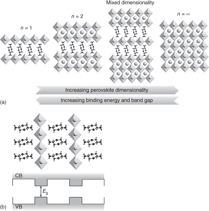
Figure 2.4.1 (a) Schematic illustration showing the crystalline structure of multidimensional perovskites, including 2D perovskites (n = 1 and 2, where n represents the metal halide lattices) and mixed‐dimensional perovskites, and 3D perovskites (n = ∞). (b) Schematic representation of the bandgap (E g) between the conduction band and the valence band (CB and VB, respectively) in 2D perovskites. Layered perovskites form multiple quantum wells, in which the inorganic and organic layers act as “well” and “barrier,” respectively.
Source: Koh et al. 2016 [6]. Copyright 2016. Adapted from Wiley‐VCH Verlag GmbH & Co. KGaA.
2.4.1.1 Multidimensional Perovskites
In general, the typical halide perovskite is defined by the general formula AMX3 (where A = Cs, CH3NH3 + or MA+, HC(NH2)2 + or FA+; M = Pb2+, Sn2+, Ge2+, Cu2+; and X = I−, Br−, Cl−) ([1]. Goldschmidt tolerance (t, Eq. 2.4.1)) and the octahedral (μ, (Eq. 2.4.2)) factors are the tools that are commonly used to determine the structural stability of perovskites by considering the ionic radii of A+, M2+, and X−. The equations are defined as follows [1], respectively:


where R A, R M, and R X refer to the corresponding ionic radii. The majority of stable “three‐dimensional” (3D) perovskites possess values of 0.8 < t < 0.9 and 0.442 < μ < 0.895, with significant deviations that result in the edge‐shared and face‐shared octahedral, instead of the pristine corner‐shared structure of the classic AMX3 perovskite [1, 2]. A number of organic ammonium cations that do not accommodate within the octahedral cavities in the 3D perovskite structure, on the other hand, adopt the “two‐dimensional” (2D) perovskite slabs with corner‐shared octahedra, and conform to the Ruddlesden–Popper formulae of A n−1A′2M n X3n+1, where A′ are typically bulkier organic ammonium cations [3, 4], whereas A, M, and X retain the same definitions. Consequently, along with the development of new organic cations, numerous perovskite materials with the general formulae (RNH3)2(A) n−1M n X3n+1 (n = integer) are now generally defined as 2D perovskites, while (RNH3)2(A) m M m X3m+2 is categorized as a 1D perovskite, where RNH3 is an aliphatic or aromatic alkylammonium cation [5]. Hence, these perovskites can be broadly classified as multidimensional perovskites (Figure 2.4.1a) [6], although the term 0D perovskites are strictly just molecular crystals and are not considered.
The corner‐shared PbX6 4− octahedra layers accommodate larger cations and the energy difference between the ionic bonding in the inorganic layers and the van der Waals forces among the organic molecules lead to the formation of self‐assembled layered perovskites that contain alternating organic and inorganic layers [7]. This unique configuration creates internal multiple quantum wells (Figure 2.4.1b) and displays interesting photophysical properties. For instance, the highest occupied molecular orbital–lowest unoccupied molecular orbital (HOMO–LUMO) energy gap of the organic ammonium cation is typically larger than the bandgap of the inorganic layers [8], and therefore the difference in the dielectric constants between these two layers creates periodic barriers and wells. Hence, these materials can be considered as containing a self‐organized multiple‐quantum‐well structure. The strong tendency to form layered perovskites and the solubility of both starting components in the same solvent has permitted a facile and convenient spin‐coating technique to deposit the thin films with homogeneous coverage on the substrate [9]. This controlled formation of layered structures has led to perovskites with larger cations and variable structures and sizes that alter the photophysical and electronic properties of these new semiconductors [10]. Adding to this versatility, mixed cations with different sizes can also form well‐organized layered structures where the smaller cations occupy voids created by the corner‐shared PbX6 4− octahedral, while the larger cations cap the stacks of inorganic layers and interleave between the 2D nanosheets [3, 11, 12]. Some prototypical examples of mixed‐dimensional perovskites are (CH3(CH2)3NH3)2(CH3NH3)2Pb3I10 and (CH3(CH2)3NH3)2(CH3NH3)3Pb4I13, which crystallized as well‐organized layered structures [6]. The properties such as the bandgap, band energy levels, carrier binding energy, and charge transport, among others, can be easily tuned simply by varying the organic cations and the thickness of the inorganic layers [6].
2.4.1.2 Multidimensional Perovskite Photovoltaics
Tremendous effort has been placed in the conventional 3D perovskites (MAPbI3, FAPbI3, for example) for their solar cell applications; however, significantly less research studies were found in multidimensional perovskite PVs. Smith et al. reported the first multidimensional perovskite solar cells (PSCs) only in 2014 [13]. They presented the first single‐crystal structure of an n = 3 perovskite, (PEA)2(MA)2[Pb3I10] (PEA + = phenethylammonium cation), derived from dark red crystals that were obtained from slow evaporation of a saturated perovskite solution. The pure n = 3 perovskite single crystal can be grown; however, the spin‐coated thin film from the lead precursor solution actually consisted of a mixture of different orders (n = 1, 2, 3, 4, and 5) in the perovskite film due to the rapid and uncontrollable self‐assembly process. These multidimensional perovskite‐based PVs exhibit overall power conversion efficiency (PCE) of 4.73%, J sc of 6.72 mA cm−2, V oc of 1.18 V, and fill factor (FF) of 0.60. Importantly, the V oc value observed here is higher than that of MAPbI3‐based solar cells, which is probably due to its slightly larger bandgap. Despite the lower efficiencies, this multidimensional perovskite displays high moisture resistance even after storage for 46 days under 52% relative humidity (RH), whereas the MAPbI3 thin film had turned from black to yellow under the same conditions (Figure 2.4.2a).
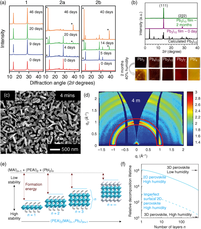
Figure 2.4.2 (a) Powder XRD patterns of films of (PEA)2(MA)2Pb3I10 (1), MAPbI3 formed from PbI2 (2a), and MAPbI3 formed from PbCl2 (2b), which were exposed to 52% RH. Films of 2a (15 minutes) and 2b (80 minutes) were annealed at 100 °C prior to humidity exposure. Asterisks denote the major reflections from PbI2. (b) XRD patterns of fresh and aged (two months) (BA)2(MA)2Pb3I10 films. The images below are the five different perovskite films before and after exposure to humidity. (c) Top‐view field emission scanning electron microscopic (FESEM) images of nanostructures of (IC2H4NH3)2(CH3NH3) n−1Pb n I3n+1 perovskites on top of mesoporous TiO2 layer from two different dipping durations in the sequential technique. (d) 2D grazing‐incidence wide‐angle X‐ray scattering (GIWAXS) data shown with a logarithmic false‐color scale. The inhomogeneous intensity distribution of the ring at q = 1 Å−1 for the four minutes sample indicates preferentially oriented crystals. (e) Unit cell structure and relative energetics of formation (i.e. stability) for (C8H9NH3)2(CH3NH3) n−1Pb n I3n+1 with different values of n. (f) DFT calculations illustrating the relative formation energy of the 2D perovskites containing different values of n under different humidity environments.
Source: Quan et al. 2016 [11]. Copyright 2016. Adapted with permission of American Chemical Society.
Source: Koh et al. 2016 [6]. Copyright 2016. Adapted from Wiley‐VCH Verlag GmbH & Co. KGaA.
Source: Cao et al. 2015 [14]. Copyright 2015. Adapted from Wiley‐VCH Verlag GmbH & Co. KGaA.
Source: Smith et al. 2014 [13]. Copyright 2014. Adapted from American Chemical Society.
Almost a year later, a second demonstration of PSCs based on multidimensional perovskites was reported by Cao et al. [14]. They synthesized a series of homologous perovskites, (BA)2(MA) n−1PbI3n+1 (BA = n‐butylammonium cation) by incorporating bulkier primary organic ammonium cations, thus confining the perovskites into a layered structure. Similarly, these perovskite thin films also contained multiple orders of perovskites as the films were simply prepared by the single‐step deposition method. The presence of mixed‐dimensional perovskites cannot be realistically avoided with the fast and low‐temperature self‐assembly processes currently utilized. The highest recorded efficiency for these multidimensional perovskites was only 4.02% with (BA)2(MA)2Pb3I10, but the perovskite film possesses high ambient stability over two months (Figure 2.4.2b). Importantly, X‐ray diffraction (XRD) analysis revealed that the lower dimensional perovskites (n = 1 and 2) tend to grow parallel to the substrate (along the (00k) and (0k0) plane), resulting in poorer charge transport in the (111) direction due to the intercalated insulating organic cation layers. Hence, stable and highly efficient multidimensional perovskites can be achieved in higher order 2D perovskites. Another key advantage of the multidimensional perovskites is their homogeneous coatings on the substrates, which were far superior to the 3D MAPbI3 counterpart films, indicating the potential for facile processing in both laboratory‐scale and large‐scale fabrication.
The nanostructuring approach to direct the growth of multidimensional perovskites is an interesting strategy to solve the charge‐transport challenges in multidimensional perovskites to create high‐efficiency and stable PSCs [6]. The insulating organic layers present in the multidimensional perovskites tend to impede the vertical charge transport, and this challenge can be addressed by growing the perovskite perpendicular to the substrate. First, a pure 2D perovskite (n = 1) was deposited by spin coating the precursor solution containing a stoichiometric ratio of lead iodide (PbI2) and iodoethylammonium iodide (IC2H4NH3I). Subsequently, the substrate was immersed into a solution containing methylammonium iodide (CH3NH3I) for different dipping durations to increase the stacking order and convert it into a mixed‐dimensional perovskite. Control of the dipping duration allows to tune the optical properties, direct the crystal growth perpendicular to the substrate, and hence improve the electrical properties (Figure 2.4.2c,d). This class of multidimensional perovskites exhibited good air stability and achieved over 9% PCE with a mixed‐cation approach [6]. More importantly, the PV devices degrade at much slower rates compared to those with MAPbI3 without any encapsulation under high RH (70–80%).
Increasing the number of stacked inorganic sheets could potentially alleviate the inferior charge transport in multidimensional PSCs. For instance, Quan et al. demonstrated the utilization of a relatively high order (n = 60) of multidimensional perovskites in PSCs, resulting in both high efficiency and stability (Figure 2.4.2e,f) [11]. The replacement of methyl ammonium iodide (MAI) with phenethylammonium iodide (PEAI) engenders higher stability owing to the latter's higher desorption energy and consequently slows down the decomposition of the perovskite film. By periodically examining the absorbance, transient photoluminescence (PL) decay, and structure (by XRD) of the perovskite films, the authors verified that the multidimensional perovskites with intercalated PEA cations possessed superior stability compared to the 3D perovskites under ambient atmospheres, likely due to the increased formation energy. The high‐efficiency MAPbI3 PSC (16.6%) deteriorated drastically to a PCE of less than 3% over eight weeks, whereas the multidimensional PVs remained stable at 11–13% PCE.
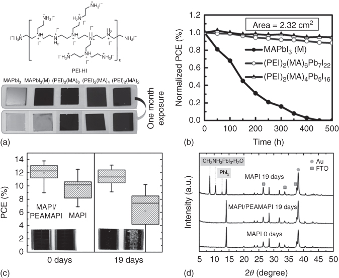
Figure 2.4.3 (a) Chemical structure of polyethylenimine hydriodide (PEI·HI) and the images of various perovskite films before and after exposure to 50% RH. (b) Stability of unsealed cells under simulated solar illumination (AM 1.5; 100 mW cm−2) during a shelf‐life investigation for 500 hours. (c) Device stability test at 75% RH in air at room temperature for 19 days. Efficiency distribution for 20 MAPbI3/(PEA)2(MA)2Pb3I10 and 20 MAPbI3 devices before and after exposure to humidity. The insets show the corresponding photograph of a MAPbI3/(PEA)2(MA)2Pb3I10 cell (left) compared to a MAPbI3 control cell (right). (d) XRD patterns of an intact MAPbI3 cell, a MAPbI3/(PEA)2(MA)2Pb3I10 cell, and a MAPbI3 cell upon exposure to moisture.
Source: Hu et al. 2016 [17]. Copyright 2016. Adapted with permission of American Chemical Society.
Source: Yao et al. 2016 [16]. Copyright 2016. Adapted with permission of American Chemical Society.
Bulkier and hydrophobic organic cations in multidimensional perovskites could strain the surface PbI bonds and repel water molecules from reactive sites in the perovskites, thereby promoting moisture resistance and prolonging the lifetime of the PSCs under ambient conditions [15]. Therefore, polymeric organic cations are also potential candidates in preparing multidimensional perovskites with high air stability. Yao et al. demonstrated the advantages of utilizing polyethylenimine hydriodide (PEI·HI) as intercalating organic cations in forming highly stable multidimensional perovskites (Figure 2.4.3a) [16]. High‐quality pinhole‐free perovskites containing polymeric cations are readily formed after the spin‐coating process, thus minimizing the shunt paths for the leakage current and offer opportunities to manufacture scalable PSCs. The strong interaction between the polymeric organic–inorganic structures led to a lower bandgap compared to smaller molecular organic cations. The scaled‐up PSCs (active area of 2.32 cm−2) with polymer‐based multidimensional perovskites exhibited PCEs exceeding 8% with excellent device lifetimes (Figure 2.4.3b).
Most recently, bilayer hybrid 2D/3D perovskites were adopted in another strategy to promote the ambient stability of the existing high‐efficiency PSCs. Generally, these kinds of bilayer hybrid structures contain high‐efficiency 3D perovskites on top of mesoporous TiO2, while lower dimensional perovskites are placed on top to enhance the moisture resistance. Docampo and coworkers deposited layered perovskites, consisting of PEA+ and MA+, on top of MAPbI3 and obtained PSCs with PCEs up to 16.8% with increased V oc and FF [17]. The perovskites capped with lower dimensional perovskites exhibited average PCEs of 11.4% after exposure to 19 days in 75% RH, whereas pure 3D perovskite devices only retained average PCEs of 6.1% (Figure 2.4.3c,d). In summary, it is clear that utilization of the multidimensional approach in perovskite PVs has significantly improved its ambient stability. However, more research effort was expected to enhance the PV efficiency of multidimensional perovskite devices while attaining ambient stability.
2.4.2 Theoretical Calculations for Pb‐Free Halide Perovskites
The concern of toxicity in typical CH3NH3PbI3 PSC triggered the intensive research in looking for a replacement for Pb. In this section, a review of the theoretical calculations and experimental validation of lead‐free halide perovskites and their solar cell applications are presented. However, it should be noted that the list of Pb‐free halide perovskites is not exclusive, because with more computational power and better understanding of the materials physics, newer horizons are being unveiled rapidly.
2.4.2.1 ASnX3 Perovskites: 3D Pb‐Free Structures
Replacing Pb2+ with Sn2+ in the perovskite structure appeared to be most viable solution toward Pb‐free perovskite for optoelectronic applications. Tin(Sn)‐based halide perovskites with ASnX3 (A = protonated cation, X = halogen element) structure is an interesting family of perovskite compounds that display temperature‐dependent phase change, bandgap tunability, ferroelectricity, and excellent optoelectronic properties, as well as composition‐dependent dimensionality [18–20]. Early studies include those by Lang et al. [21] who explored the electronic and optical properties of Sn‐ and Pb‐based perovskites using standard density functional theory (DFT) and found that all these compounds possess a similar electronic structure, expecting similar electronic behavior. However, the inherent instability of Sn2+ cation in the atmospheric conditions leads to poor performance as solar cell absorber materials. Theoretical investigations on Sn‐based inorganic halide perovskites had begun as early as the 1980s due to their interesting temperature‐dependent phase transitions. Sn‐based halide perovskites undergo several phase transitions from a high‐temperature cubic phase toward a lower symmetry structure with decreasing temperature. These phase changes are associated with increasing packing density through distortion and rotation of SnX6 octahedra, rather than a complete reordering of the atoms [22, 23]. Some earlier reports also claimed that the stereochemically active lone pair electron of tin had a key role to play in the distorted low‐temperature phases [24]. Initially, the cubic CsSnBr3 was thought to be semimetallic based on semiempirical extended Huckel theory (EHT) calculations [25]. Although this method is quite satisfactory for describing valence band structure, EHT performs poorly in describing the conduction band nature. Lefebvre et al. [26] performed band structure calculations based on the pseudopotential approach, which gives a better description of lowest conduction band along with valence electrons. Interestingly, they found CsSnBr3 to be a zero‐bandgap compound even without considering the spin‐orbit coupling (SOC) effect. However, these results do not agree with experimental values. The bandgap problem was somewhat corrected by Bose et al. [27] when they performed a scalar‐relativistic muffin‐tin‐orbital calculation based on local density approximation (LDA) within the framework of DFT and concluded that CsSnBr3 is a narrow bandgap semiconductor with a direct bandgap of 0.26 eV. Considering the use of LDA, it can be fairly assumed that the original bandgap should be much higher than that. Their simulation also indicated that the valence band of CsSnBr3 is a mixture of Sn 5s and Br 4p orbitals and the role of Cs+ is negligible in the band edges. However, there was no change in the bandgap due to a low‐temperature structural change in the perovskite. In 2008, Borriello et al. [23] performed ab initio calculations based on DFT using the generalized gradient approximation (GGA) for exchange correlation energy on several ASnX3 compounds (A = Cs, CH3NH3, NH2CHNH2, X = Cl, I). They have shown that in the high‐temperature cubic phase, the A site cation has little role in determining the band edges of Sn‐based halide perovskites. They concluded that the A site (organic or inorganic) cations mainly control the crystal structure of the perovskite, which has a drastic effect on the bandgap of the compound. For example, phase change in CsSnI3 is associated with progressive tilting of SnI6 octahedra along the ab‐plane, without any observable change in SnI bond length or the angle (Figure 2.4.4a,b). Hence, all the phases of CsSnI3 exhibit direct bandgap, which gradually increases with progressive tilting of the SnI6 octahedra. Even replacing Cs+ with MA or FO does not change the crystal symmetry at room temperature. On the other hand, the phase change in CsSnCl3 is associated with the drastic change in the crystal structure, from a corner‐sharing octahedral network (high‐temperature cubic phase) to almost isolated edge‐sharing octahedral chain network (low‐temperature monoclinic phase), resulting in a much wider bandgap and an anisotropic valence band. Interestingly, the hybrid analogous MASnCl3 preserves the corner‐sharing octahedra even at low temperature, which is attributed to the steric interaction between the inorganic cage and larger organic cation. The role of the A site cation thus can be generalized only as the electron donor, as neither the organic nor inorganic cations play any role in the valence band maximum (VBM) or conduction band minimum (CBM). The change in bandgap can then be explained easily by the change in lattice constant originating from different cation sizes (Figure 2.4.4c).

Figure 2.4.4 (a) A perspective of CsSnI3 in the tetragonal phase and (b) orthorhombic phase, (c) The energy bandgap as a function of the cubic lattice a. The black circles represent the calculated band gap for a perfect cubic perovskite CsSnI3 with different lattice parameters. The squares represent the bandgap of CsSnI3 in the three phases, and the bandgap of MASnI3 and of FOSnI3 in the cubic phase.
Source: Borriello et al. 2008 [23]. Copyright 2008. Adapted with permission of American Physical Society.
After the emergence of PSC, Sn‐based halide perovskites, especially CsSnI3 and its hybrid compound MASnI3 returned to the spotlight due to interesting optoelectronic properties such as p‐type metallic conductivity and strong luminescence. As the standard DFT calculations are not reliable in predicting the bandgap of semiconductors, Huang and Lambrecht [28] reinvestigated the electronic structure of cubic phase CsSnX3 (X = Cl, Br, I) using quasiparticle self‐consistent GW (QSGW) method. In general, the QSGW method has been proved to be very accurate and reliable for describing the band structure and excited‐state properties for weakly correlated systems. They found that the bandgap is essentially controlled by Sn s to I p covalent antibonding interaction which is expected to be weaker with increasing lattice constant, resulting in a wider bandgap with increasing cell volume. On the other hand, the bandgap is expected to increase from Cl to I due to lower energetic anion p levels. However, the opposing SOC effect in heavier halogen atoms further compensates the increase in bandgap, and the total effect on bandgap due to the change in halogen atoms is quite small. An interesting finding from their work is that the exciton binding energy of CsSnI3 was found to be around 0.1 meV, which is two orders smaller than the experimentally reported value of 18 meV [29]. The authors argued that the reported value of exciton binding energy can only be interpreted as exciton linewidth or the energy of bound exciton, as the free exciton binding energy should be lower than that. Based on the band structure, the effective masses of hole and electrons were found to be small and decreased from Cl to I. However, nearly equal effective hole and electron mass failed to explain the p‐type conductivity in CsSnI3. Defect characteristics studies by Chung et al. [20] shed light on the origin of the p‐type conductivity. The role of defects in the optoelectronic properties of the solution‐processable semiconductor is crucial as the defects are in thermodynamic equilibrium with the constituents. The defect formation energy can be calculated using first‐principles calculations based on the supercell approach. An excellent review on defect formation energy calculations can be found in Freysoldt et al. [30]. Figure 2.4.5 illustrates the intrinsic defect formation energy as a function of Fermi level in three different growth conditions. The p‐type conductivity eventually arises from the Sn vacancies (V Sn), which is the most favorable intrinsic defect in CsSnI3. The strong luminescence at near‐band edge can also be explained by the V Sn‐modulated defect centers. The presence of V Sn as deep‐level defects were also confirmed by Kumar et al. [31]. In addition to PV applications, Sn‐based halide perovskite, especially formamidinium tin iodide (FASnI3), has been shown to display excellent ferroelectric properties. Based on first‐principles calculations, polarization of FASnI3 can be changed depending upon the spatial arrangement of FA+ cation [32].

Figure 2.4.5 Calculated defect formation energies for V Sn, V Cs, SnI, and V I in the cubic CsSnI3. Charge state, q, is denoted by +, 0, and −. The energy level of the VBM is set to zero. The regions below VBM and above CBM are shaded in gray. The defect formation energies of SnI are higher than 2.5 eV in the Sn‐poor, I‐rich and the Cs‐poor, I‐rich conditions.
Source: Chung et al. 2012 [20]. Copyright 2012. Adapted with permission of American Chemical Society.
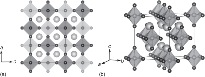
Figure 2.4.6 (a,b) Crystal structure of the vacancy‐ordered double perovskites, Cs2SnI6.
Source: Maughan et al. 2016 [33]. Copyright 2016. Adapted with permission of American Chemical Society.
2.4.2.2 A2SnX6 Perovskites: Metal‐Deficient Structures
Although the electronic and optical properties of Sn‐based halide perovskites are quite tempting, poor stability of Sn2+ limits the extensive applications. Sn2+ in perovskite structure can readily be oxidized into Sn4+, which ushers in an alternate class of perovskites. The use of tetravalent Sn4+ to replace divalent Pb2+ results in a vacancy‐ordered perovskite structure to maintain the charge balance (Figure 2.4.6). It can also be visualized as the ordered double perovskites with the general formula A2B′B″X6 in which one B‐site cation is replaced with a vacancy (A2B□X6). However, there is some ambiguity as to whether such simple ionic model can be applied for complex salts [22, 34]. From first‐principles calculations, Sn 5s was found to be well below the Fermi level and the corresponding Bader charge analysis suggests the divalent nature of Sn [34, 35]. First‐principles calculations based on the self‐consistent, full‐potential linearized augmented plane wave (LAPW) method within DFT, using the GGA‐PBE (Perdew‐Burke‐Ernzerhof) for the exchange and correlation potential, resulted in a direct bandgap of ∼1.3 eV, which is in excellent agreement with the experimental values [36]. It should be noted that the bandgap correction was done using the modified Becke–Johnson exchange potential. Later, Saparov et al. [37] reported an experimental bandgap of 1.6 eV and calculated bandgaps of 1.27 and 1.62 eV with (Heyd‐Scuseria‐Ernzerhof) HSE06 hybrid functional with 34% and 37% exchange, respectively. However, the use of SOC was not mentioned in the calculation. Maughan et al. [33] carried out electronic band structure calculations in a similar manner, but with explicit treatment of SOC and found a direct bandgap of 0.97 eV. Their GW0 calculation, which is more sophisticated than hybrid calculations, also indicated a bandgap of 0.88 eV. Hence, the experimental bandgap of 1.6 eV may be influenced by some secondary phase formation, which is quite common in complex perovskite semiconductors. Moving on from the bandgap discrepancy, the nature of charge carriers is also different between Cs2SnI6 and CsSnI3, where the former shows n‐type conductivity and the latter shows p‐type. This could be explained by the defect characteristics. The formation energies of iodine vacancies are quite small (0.14–0.39 eV depending upon the chemical potential) and the 0/1 transition states are located just 0.07 eV below the VBM, which is most likely the source of n‐type conductivities [33].
2.4.2.3 Germanium‐Based Perovskites
Like Pb‐ and Sn‐based halide perovskites, theoretical investigations on germanium (Ge)‐based halide perovskites began even before the realization of their potential applications in PVs. Unlike Pb‐ and Sn‐based halide perovskites, the smaller ionic radius of Ge2+ as well as the presence of stereochemically active 4s2 electron pair hinders the formation of stable cubic perovskites in room temperature. Hence, the GeX6 octahedra is distorted drastically to form a pyramidal structure symmetry, which is expected to exhibit nonlinear optical properties. However, Ge‐based perovskites also exhibit rich structural diversity depending on the temperature and protonated cation. For example, CsGeI3 transforms from rhombohedral phase into cubic (Pmmm) symmetry above 290 °C. The band structure calculated by Li‐Chuan et al. [38] following the standard DFT approach with LDA as exchange correlational functional shows similar orbital characteristics as that of Pb‐ or Sn‐based halide perovskites. However, the bandgap seemed to be underestimated severely due to use of LDA. Follow‐up calculations also reveal the increase in bandgap from I to Cl, which is in good agreement with the experimental trends [39]. However, the potential of Ge‐based halide perovskites in solar cell absorber materials were not fully realized until Stoumpos et al. [40], and Krishnamoorthy et al. [19] synthesized organic‐cation‐based Ge iodide perovskites. Although the role of organic cation is limited to the crystal motif's formation as the interaction with inorganic network is negligible, the charge carrier properties among different hybrid Ge iodide perovskites vary significantly [41]. In comparison to Sn‐ or Pb‐based halide perovskites, the values of effective mass are much higher for similar calculations, but comparable to other thin‐film semiconductors. Sun et al. [42] studied the effect of systematic replacement of Pb2+ from MAPbI3 with Ge2+ using DFT at different calculation levels. The incorporation of Ge2+ in place of Pb2+ displays gradual constriction in lattice constants and increase in lattice deformations. The change in bandgap is severely affected by the SOC effect for Pb2+, while for the lighter Ge2+ the effect is minimal (Figure 2.4.7a). The optical absorption coefficients of mixed Pb/Ge perovskites calculated from first‐principles calculations is projected to be higher than those of either MAGeI3 or MAPbI3. However, the change in orbital characteristics near the band edges is also minimal, except for a sharp increase of Ge p orbital in the CBM at the expense of Pb p orbital contribution. As for charge‐transport properties, the change in average electron and hole effective masses are shown in Figure 2.4.7b. Among the studied Ge/Pb iodide perovskites, MAGe0.75Pb0.25I3 shows best transport properties with nearly balanced electron and hole effective mass.

Figure 2.4.7 (a) Experimental and calculated bandgap trends with different methods. (b) The calculated average electron and hole effective masses of MAGe x Pb(1−x)I3 structures as a function of proportion x. The effective masses were calculated from HSE‐SOC band structure.
Source: Sum et al. 2016 [42]. Reproduced with permission of PCCP Owner Societies.

Figure 2.4.8 (a) The structure of the three‐layer (101) MAGeI3 surface slab with possible locations of adsorbed H2O. (b) The decomposition pathway for one MAGeI3 molecule under water attack.
Source: Sun et al. 2016 [43]. Reproduced with permission of PCCP Owner Societies.
Nevertheless, the main challenge associated with Ge‐based perovskites is its stability in ambient atmosphere. Ge‐based perovskites readily decompose in the presence of ambient atmosphere. Sun et al. [43] investigated the effect of water (H2O) molecule on the MAGeI3 surface based on first‐principles calculations. They found that H2O molecules can easily diffuse through the surface of the MAGeI3. The most stable surface of MAGeI3 was found to be (101) plane, which is composed of GeI dangling bonds with iodine atoms exposed on the surface. The MA+ cations reside inside the voids of the inorganic cage compensating the charge balance (Figure 2.4.8a). Initially, a single water molecule is adsorbed on the surface of MAGeI3 through hydrogen bonding connected with O(H2O) and H with nearest MA+ cation (region O in Figure 2.4.8a). Surprisingly, with increasing number of water molecule near the surface, the adsorption energy decreases from −0.1 eV for one H2O molecule to a minimum of −0.27 eV for six water molecules. When the number of water molecules increases to more than six, the intermolecular hydrogen bonding becomes stronger, resulting in a decrease in the hydrogen bond strength between H2O molecules and MA+ cations of the perovskite, corresponding to a greater adsorption energy. However, to degrade the perovskite completely, the water molecule needs to diffuse first through the dangling bond region (region F in Figure 2.4.8a). The energy of one water molecule inside the dangling bond region was found to be much lower than the adsorption energy with an activation barrier as little as 0.09 eV. As a consequence, water molecules are most likely to stay inside that region and the adsorption on the surface can proceed in the forward direction easily. For further penetration inside the MAGeI3 crystal, the water molecule then needs to pass through the I–Ge–I inorganic network (region S in Figure 2.4.6). The energy barrier for that transition state was found to be 0.43 eV, which is still quite small. Based on their calculation, the authors proposed the following mechanism (Figure 2.4.8b):
- The degradation of MAGeI3 starts as soon as the inorganic network of GeI2 begins to be damaged by hydration of the phase.

The hydrated phase exists for N ≤ 2.
- As soon as another water molecule is adsorbed, the perovskite surface starts degrading with release of CH3NH2 gas.
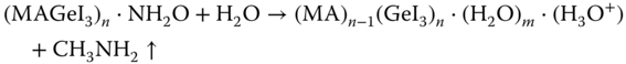
- With increasing number of water molecules on the surface, the GeI bonds start to break due to stronger H‐binding with I− anion.
- The new hydrate generated in step 2 will continue to degrade with the release of HI
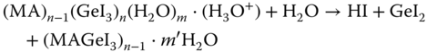
- In humid atmosphere, the continuous adsorption of the water molecule will continue the release of CH3NH2, resulting in the degradation of the perovskite.
2.4.2.4 Bismuth/Antimony‐Based Perovskites
The excellent optoelectronic properties of lead‐based halide perovskites is often linked with the presence of 6s2 lone pair electrons. Group 15 elements, especially Bi3+ and Sb3+, also possess an electronic structure similar to that of Pb2+ due to which similar optoelectronic properties are expected. Since these elements exist in the stable +3 oxidation state, it is difficult to accommodate Bi3+ or Sb3+ inside the conventional AMX3 perovskite structure. Previous studies on Bi/Sb‐based ternary halide compounds had mostly focused on single‐crystal properties, ferroelectricity, phase transformations, and nonlinear optical properties [44]. Recently, the interest in these compounds has been renewed due to their potential applications in PVs. The electronic structure calculations for Bi‐ and Sb‐based ternary halides have shown remarkable similarities in band edge characteristics to that of Pb‐based halide perovskites [45]. Contrary to conventional semiconductors such as Si or GaAs, the CBM and VBM of [PbI6]4− cluster are antibonding in nature, contributed by the partially oxidized Pb2+ cation and PbI antibonding orbital, respectively [46]. For the Bi/Sb‐based ternary halide perovskite, a similar VBM nature is expected due to lone pair 6s2 electrons [47]. The contribution of A+ cation on VBM and CBM is also negligible as the band edges are formed by the Sb/BiI bonding. Analogous observations can also be found for conventional Pb‐halide perovskites, where the influence of +1 cation is negligible on the VBM and CBM characteristics [48]. So the electronic structures of inorganic Bi/Sb‐based ternary halides can represent the family justly. The valence band of Cs3Sb2I9 is mainly contributed by the p orbital of I and partly by Sb(s). These antibonding characteristics of VBM are expected to suppress the valence‐band‐derived states such as cation vacancies. The nature of the CBM, on the other hand, is quite different and is dependent on the crystal structure (dimer or layered). For example, the electronic structure of Cs3Bi2I9 and Cs3Sb2I9 dimer phase exhibits remarkable similarities as both possess indirect bandgap and similar conduction band features. While conduction band is mostly Pb(p)/Sb(p) characteristics in Pb‐based and Sb‐based ternary halides (layered structure), respectively, a mixture of I(p) and Bi(p)/Sb(p) orbitals dominates the CBM of dimer Cs3Bi2I9/Cs3Sb2I9. The p‐orbital characteristics of both valence and conduction bands lead to high joint density of states, resulting in an unusually large absorption coefficient for both Bi‐ and Sb‐based ternary halides. Although the layered structure of Cs3Sb2I9 is more promising in terms of optoelectronic properties than in its dimer structure, the latter is more favorable to form under normal processing conditions. However, one possible way to solve the problem is to replace Cs with smaller cations. For example, Rb3M2I9 (M = Sb3+, Bi3+) essentially forms the layered structure even under normal processing conditions and exhibits better optoelectronic properties than the homologous dimer structure [49]. The electronic structure calculations further reveals a flat band structure for both the Sb‐ and Bi‐based dimer phase, which can be attributed to the heavy effective mass of the carriers [47, 50]. In addition, Sb‐ and Bi‐based ternary halide compounds have lower crystal symmetry as compared to Pb‐based halide perovskite, which leads to anisotropic charge transfer. In addition, most of the intrinsic defects (except Cs vacancy and interstitial Cs) in Cs3Sb2I9 form deep level states in the bandgap which can act as non‐radiative recombination centers in optoelectronic applications. This could be explained on the basis of the orbital characteristics of the compound. The Sb p orbital is more localized than the Pb p orbital, resulting in stronger Sb p−I p antibonding than the Pb p−I p antibonding, which in turn implies that the energy difference between the anion's p orbital and the CBM is larger for Cs3Sb2I9 than for CH3NH3PbI3.This results in mid‐bandgap states of the donor defects. On the other hand, weaker s–p antibonding coupling is the primary reason for deep acceptor defects. In addition to that, defect characteristics also reveal the transition from p‐type conductivity to n‐type conductivity when the crystal growth conditions can be tuned from I‐rich/Sb‐poor to Sb‐rich/I‐poor conditions.
2.4.2.5 Double Perovskites: Hybrid Binary Metal Structures
Instead of a single divalent element, one monovalent and one trivalent element can replace two Pb2+ from the halide perovskite structure. The idea of double perovskites is not new, with the analogous oxide structures having been examined for a long time. Such atomic transmutation has been successful in even thin‐film solar cell application such as the copper zinc tin sulfide (CZTS) systems. Following a similar strategy, a Pb‐free halide perovskite family with the formula A2M+M3+X6 has received attention among the halide PV community. Giorgi and Yamashita [51] studied the MATl0.5Bi0.5I3 and MAIn0.5Bi0.5I3 based on DFT calculations and found striking similarities in electronic structure with Pb‐based halide perovskites. The bandgaps of the compounds are 1.68 and 1.03 eV, respectively, as per PBE/PAW (projector augmented wave)‐level calculations. More recently, successful synthesis of Cs2AgBiBr6 and Cs2AgBiCl6 enabled detailed theoretical understanding of these types of materials [52, 53]. The bandgap of the Bi‐based halide double perovskites are quite similar to lead‐based halide perovskites, however indirect in nature [53]. The valence band is composed primarily of the halogen p orbital and the conduction band formed by the antibonding of Ag 5s and Bi 6p states. The main problem is the admixture of Ag d orbital in the valence band, which is partially responsible for the indirect bandgap. Later, Zhao et al. [54] identified 11 potential halide double perovskites based on first‐principles calculations. For the M3+ cation, Bi3+ and Sb3+ cations were considered due to the similar electronic structure as that of Pb2+. For the M+ cation, they considered group IA (Na+, K+, Rb+)/group IB (Cu+, Ag+, Au+)/group IIIA (In+, Tl+) elements (Figure 2.4.9). They used four criteria to screen the perovskite compounds such as decomposition enthalpy (>0), bandgap (0.8–2 eV), effective mass (<1.0 m0), and exciton binding energy (<100 meV). Out of all the combinations, they successfully found 11 optimal halide double perovskite compounds such as Cs2CuSbCl6, Cs2CuSbBr6, Cs2CuBiBr6, Cs2AgSbBr6, Cs2AgSbI6, Cs2AgBiI6, Cs2AuSbCl6, Cs2AuBiCl6, Cs2AuBiBr6, Cs2InSbCl6, and Cs2InBiCl6. Among these compounds, the first nine compounds exhibit indirect bandgap, while the bandgaps of the two In+ based double perovskites are direct in nature. In a similar manner, Pb2+ and two I− can be transmuted into one M3+ and one Ch2− (chalcogenide) anions, leading to I–III–VI–VII2 structure. Sun et al. [55] calculated the electronic band structure of Bi‐ and Sb‐based chalcogenide‐halide perovskites and found that these compounds are promising PV materials in terms of bandgap. However, subsequent reports indicate that none of these materials are thermodynamically stable as they will be prone to decomposition into other binary or ternary phases [56].

Figure 2.4.9 (a) Space of candidate A2M+M3+X6 perovskites for materials screening: left panel shows adopted double‐perovskite structure, and right panel shows schematic idea of atomic transmutation. (b) Materials screening process by considering gradually the properties relevant to photovoltaic performance, i.e. decomposition enthalpy (ΔH), bandgap, carrier effective masses (m e*, m h*), and exciton binding energy (ΔE b). The red squares mean the materials passing the screening (selected) and the green ones mean not passing (abandoned). The optimal nontoxic A2M+M3+X6 perovskites satisfying all the criterions are marked with red checks.
Source: Zhao et al. 2017 [54]. Copyright 2017. Adapted with permission of American Chemical Society.
2.4.3 Experimental Efforts in Pb‐Free Perovskite Photovoltaics
Most of the efforts to replace lead in perovskite halides were focused on elements in the same group or adjacent groups such as Sn, Ge, Bi, and Sb assuming that similar electronic configurations will lead to similar optoelectronic properties. Suitable oxidation states, ionic sizes, and the presence of ns2 electrons which result in the defect‐tolerant properties of lead are the major criteria in the search for the replacements.
2.4.3.1 Sn2+ and Ge2+ as Replacements for Pb2+ Ge$^{2+}$ replacements for Pb$^{2+}$"?>
As discussed earlier, tin with an electronic configuration [Kr] 4d10 5s2 5p2 is very similar to lead and hence was considered first as its most potential replacement. The first report on tin‐based perovskites in a solar cell was on CH3NH3SnI3 with an efficiency of 6.4% [18a] formed by spin coating SnI2 and CH3NH3I in dimethylformamide (DMF) in an inert atmosphere. The device exhibited a reasonable open circuit voltage of 0.88 V considering its low bandgap of 1.23 eV. However, these were very unstable in air due to oxidation of +2 Sn to +4 states, resulting in a large spread in the device efficiencies with much of the solar cells showing very low power conversion efficiencies. The presence of +4 Sn also resulted in variable self‐doping of the material, resulting in a high hole‐doping density of ∼1018 cm−3. The recombination with these self‐doped carriers limited the diffusion lengths to only 30 nm, significantly lower than MAPbI3. It was suggested that reducing these background carriers could be an effective strategy to improve the performances by improving the diffusion lengths. Another interesting development in the area of Sn perovskites was the use of a mixed metal cation with lead (CH3NH3Pb1−x Sn x I3) [57]. This resulted in anomalous behavior, with the mixed perovskite exhibiting a bandgap lower than either the pure Pb‐ or Sn‐based perovskites, thus extending the absorption range to near infrared (1050 nm). In another work, the same group investigated the possibility of a mixed halide Sn perovskite – MASnI3−x Br x [18b] – in order to tune the bandgap of the material. The highest power conversion efficiency realized was 5.73% for CH3NH3SnIBr2.

Figure 2.4.10 (a) Viability of tuning the bandgap of lead‐free perovskites by anion mixing. (b) Strategies to develop lead‐free halide perovskites. (c) Structural variants existing within the A3M2X9 composition.
Source: Harikesh et al. 2016 [49]. Copyright 2016. Adapted with permission of American Chemical Society.
Source: Giustino and Snaith 2016 [59]. Copyright 2016. Adapted with permission of American Chemical Society.
Source: Sabba et al. 2015 [58]. Copyright 2015. Adapted with permission of American Chemical Society.
The first report on fully inorganic Sn‐based perovskite was on CsSnI3 [31] with a power conversion efficiency of 2.02%. It was found that the pristine CsSnI3 exhibited very poor PV performance due to the presence of Sn vacancies. These tin vacancies were passivated by addition of 20% SnF2 to attain good PV performance. This was also reflected in the reduction of carrier density of 1019 cm−3 in pristine sample to 1017 cm−3 with 20% SnF2 addition. The excess SnF2 increases the Sn chemical potential, leading to increase in formation energy of Sn vacancies and a decreased concentration of these defects. The background carrier density of 1017 cm−3 is still very high compared to CH3NH3PbI3 (with carrier densities of 109–1011 cm−3), which could be the reason for the limited V oc of 240 mV in the champion device. Higher open circuit voltages were obtained by opening up the bandgap through halide substitution, although power conversion efficiencies were still limited [58]. The bandgap of CsSnI1−x Br x was tuned between 1.27 and 1.75 eV (Figure 2.4.10a) with a reduction in charge carrier densities to 6.3 × 1015 cm−3 for CsSnIBr2. Another strategy to tune the bandgap of the Sn perovskite is to change the A cation. Formamidinium‐based Sn perovskites crystallize in an orthorhombic (Amm2) crystal structure and exhibit a slightly higher bandgap of 1.41 eV, which is close to the optimum value for single‐junction solar cells. FASnI3‐based solar cells were fabricated with an efficiency of 2.1% [60] by again utilizing the SnF2 addition to reduce tin vacancies. However, the low solubility of SnF2 in DMF resulting in phase separation is a limiting factor to achieve higher voltage. Another report on the same material suggests that the solubility of SnF2 in DMF can be improved by addition of pyrazine [61], which can form a complex with SnF2. This avoids phase separation and yielded perovskite films with full coverage on TiO2, improving the efficiency to 4.8%.There are also reports on Cs‐ and FA‐based Sn perovskites on inverted architectures, albeit with lower efficiencies [62]. In addition to the challenges rendered by tin oxidation, morphology control of these tin halide perovskites is challenging. The rapid crystallization of the Sn perovskite with DMF as solvent limits the ability to form pinhole‐free film by spin coating and limiting the open circuit voltage. A systematic study of various solvents (DMF, dimethyl sulfoxide (DMSO), N‐methylpyrollidone (NMP)) suggested that DMSO could be a better alternative to the commonly used DMF [63] in obtaining higher quality films. The reason is the ability to coordinate strongly to the SnI2, forming an adduct of formula SnI2·3DMSO. This adduct allows the MAI ions to react with SnI2 in a controlled manner limited by the rate of DMSO removal to obtain controlled crystallization and uniform coverage.
Moving even further up in the group of the periodic table, the smaller Germanium was also investigated as a potential candidate to form perovskites with PV properties. CsGeI3, MAGeI3, and FAGeI3 exhibit a bandgap of 1.63, 2.0, and 2.35 eV, respectively [64]. All of them crystallize in rhombohedral symmetry at room temperature. However, solar cells of CsGeI3 and MAGeI3 suffered from a very low V oc of 74 and 150 mV, respectively, restricting the efficiencies to 0.11% and 0.2% only. Germanium is even more unstable compared to Sn and gets easily oxidized to the +4 state, which is the reason for the poor performance. The problem is aggravated by its poor solubility in polar solvents, which restricts good film formation.
Most of the research on lead replacement was focused on Sn or Ge in the same group. However, it is known that the inert pair effect responsible for the stability of the +2 state of lead reduces as we move up in the group. Thus, Sn2+ and Ge2+ are very unstable and gets oxidized to +4 ions. These +4 ions can act as traps leading to recombination and hence limit the performances. Furthermore, reports show that Sn perovskites can be even more toxic compared to lead due to its potential oxidation to the +4 oxidation state releasing HI into the environment [65]. This necessitated expanding the search to other group elements and other perovskite derivatives as well.
Table 2.4.1 Reported optoelectronic characteristics of Cs2SnI6.
| References | Bandgap (eV) | Carrier density (cm−3)/type | Mobility (cm2 V−1 s−1) |
| Lee et al. [36] | 1.3 (direct) | 1 × 10¹⁴ (n) | 310 |
| Lee et al. [36] | 1.3 (direct) | 1 × 10¹⁴ (p) | 42 |
| Saparov et al. [37] | 1.6 (direct) | 6 × 10¹⁶ (n) | 2.9 |
2.4.3.2 A2SnX6 as a Stable Alternative to ASnX3 alternative to ASnX$_{3}$"?>
The use of tetravalent Sn is a strategy to enhance the stability of the Sn perovskite. However, a +4 Sn can only form compounds of structure A2SnX6, which is considered a 0D perovskite structure with isolated (SnI6)2− octahedra (Figure 2.4.10b) [59]. There are several reports utilizing Cs2SnI6 as a hole‐transporting material in dye‐sensitized solar cells due to its exceptional p‐type conductivity [36, 66]. However, the reports on the bandgap, carrier densities, mobility, and type of charge carriers are still inconclusive, as shown in Table 2.4.1. It is claimed that the pristine material is n‐type and the reported p‐type behavior is caused by doping with Sn2+. Nevertheless, the optimum bandgap of 1.3–1.6 eV of the material makes it interesting as an absorber for solar cells. The only report (so far) of Cs2SnI6 as a solar cell absorber material is by utilizing ZnO nanorods as electron‐transporting layer and poly(3‐hexylthiophene‐2,5‐diyl) (P3HT) as hole transporting material (HTM) reaching an efficiency ∼1% [67].
2.4.3.3 Cu2+: an Alternative Divalent Metal Cation
If one excludes group 14 elements, the next alternatives are the transition metals due to their ability to form +2 oxidation states essential for AMX3 halide perovskite structures. However, the small size of the transition metal cations limits their ability to form corner‐sharing structures. Instead, most of them form linear chains of face‐sharing octahedra which might seriously affect the charge transport in these class of compounds. In addition, most of the transition metal halides are moisture sensitive as well. However, one alternative is to form 2D perovskites of the structure A2MX4 exhibited by metal ions such as Cu2+, Ni2+, Co2+, Fe2+, etc. Some research groups have investigated 2D perovskites of Cu for application in solar cells due to their stable +2 oxidation state in aerobic environment and good absorption in visible region. A detailed analysis of the copper perovskites of the structure (CH3NH3)2CuCl x Br4−x revealed that the presence of Cl is essential to stabilize the system against copper reduction and enhance crystallization [1a]. In addition, changing the Br/Cl ratio helped tune the absorption within the visible to near‐infrared range. However, the solar cells fabricated were limited by low V oc and short circuit current densities. The low absorption coefficient and the heavy mass of the holes arising from the layered nature of the material were found to be the reasons for this poor performance. In addition, the paper also discussed the probability of Cu+ formation, which could act as potential traps. Copper‐based 2D perovskites of the structure: (p‐F‐C6H5C2H4‐NH3)2CuBr4, and (CH3(CH2)3NH3)2CuBr4 [68] were also demonstrated as solar cell absorbers albeit with very low efficiencies.
The poor performance of copper perovskites may also be due to the absence of the outer ns2 electrons, which provide the defect tolerance and the dispersive valence band in case of lead. Thus, a more logical strategy is to search for compounds with outer ns2 electrons. This necessitates looking for elements with other oxidation states as well rather than confining to +2.
2.4.3.4 Bi3+ and Sb3+: Toward Trivalent Metal Cations Sb$^{3+}$, trivalent metal cations"?>
As discussed earlier, Bi3+ and Sb3+ which have electronic configuration similar to that of Pb2+ are other viable alternatives. The presence of ns2 electrons must also equip them with the defect‐tolerant property of lead. However, the +3 state constrains their ability to form a 3D corner‐sharing perovskite structure. Instead, they form A3Sb2X9 compounds with a dimer structure (with fused bi‐octahedron) or a layered structure (with corner‐sharing octahedron).The first report on bismuth‐based perovskite was on Cs3Bi2I9 with an efficiency of ∼1% [69]. The material consisted of fused bi‐octahedral (Bi2I9)3− clusters surrounded by Cs atoms. It is claimed to be nontoxic and was reported to be stable over a month, with no noticeable reduction in efficiency when stored at humidity less than 10%. The PL and PV performance of MA3Bi2I9 was found to be very low compared to Cs3Bi2I9 consistent with the other reports on MA3Bi2I9 solar cells with a low efficiency of 0.19% [70]. MA3Bi2I9 exhibited p‐type conductivity with a carrier density of 1016 cm−3 and mobility of 1 cm2 V−1 s−1. This high background carrier density was suspected to have contributed to bulk recombination, leading to a low V oc of 0.35 V. Other reports attribute the lower performance to poor morphology of the MA3Bi2I9 layer, with the efficiency influenced by the underlying mesoporous TiO2 layer [71]. The devices made on anatase TiO2 mesoporous layer showed better performance than those on a mesoporous brookite TiO2 layer or a planar architecture. A detailed material study on MA3Bi2I9 [72] suggested that post treatment with pyridine can improve the PL lifetime of the material possibly by passivation of under‐coordinated bismuth ions on the surface. A maximum PL lifetime of 0.76 ns was achieved, depending on the processing technique adopted. This is encouraging because materials with <1 ns lifetimes have been reported to achieve efficiencies close to 10% [73]. Interestingly, double perovskites of the formula Cs2AgBiBr6 exhibited extraordinary PL lifetimes of 660 ns, which are on par with MAPbI3, substantiating the defect‐tolerant property of bismuth. In addition, the compound was found to exhibit extraordinary stability in moisture and light exposure even after one month. However, the presence of Ag seriously inhibits the solution processability of the material. The potential of bismuth halides as potential replacement is also corroborated by the AgBi2I7 solar cells with efficiency of 1.22% [74] and BiI3‐based solar cells with efficiency of 0.3% [75, 76].
There are also reports of A3M2X9 structures based on Sb as viable PV materials. However, the highest efficiency reported till date is only 0.5% with MA3Sb2I9 as absorber [77]. It is claimed that the layered structure of A3Sb2I9 should exhibit better optoelectronic properties compared to the dimer form from first‐principles calculations [47]. However, the lack of solution processability of the structure is a bottleneck to its formation. In addition, the material is also susceptible to various defects which can induce deep traps, limiting the PV performance. A smaller cation like Rb was found to template the formation of the layered phase even via a solution process [49] (Figure 2.4.10c). However, the presence of deep defects possibly limited the device performance. Thus, a strict control over the stoichiometry using optimum fabrication conditions will be necessary to obtain good performance with these classes of compounds (Table 2.4.2).
Table 2.4.2 Highest reported photovoltaic characteristics of lead‐free halides.
| Material | Device architecture | η (%) | J sc (mA cm−2) | V oc (V) | FF |
| MASnI3 [18a] | FTO/bl‐TiO2/TiO2/MASnI3/HTM/Au | 6.4 | 16.8 | 0.88 | 0.42 |
| CsSnI3 [31] | FTO/bl‐TiO2/TiO2/CsSnI3/HTM/Au | 2.02 | 22.7 | 0.24 | 0.37 |
| FASnI3 [61] | FTO/bl‐TiO2/TiO2/FASnI3/HTM/Au | 4.8 | 23.7 | 0.32 | 0.63 |
| Cs2SnI6 [67] | FTO/bl‐ZnO/ZnO‐NR/Cs2SnI6/P3HT/Ag | 0.86 | 3.2 | 0.52 | 0.52 |
| MAGeI3 [64] | FTO/bl‐TiO2/TiO2/CsGeI3/HTM/Au | 0.20 | 4.0 | 0.15 | 0.30 |
| Cs3Bi2I9 [69] | FTO/bl‐TiO2/TiO2/Cs3Bi2I9/HTM/Au | 1.0 | 2.15 | 0.85 | 0.60 |
| MA3Bi2I9 [71] | FTO/bl‐TiO2/TiO2/MA3Bi2I9/HTM/Au | 0.25 | 0.83 | 0.56 | 0.48 |
| AgBi2I7 [74] | FTO/bl‐TiO2/TiO2/AgBi2I7/P3HT/Au | 1.22 | 3.3 | 0.56 | 0.67 |
| Ag2BiI5 [78] | FTO/bl‐TiO2/TiO2/Ag2BiI5/P3HT/Au | 2.1 | 6.8 | 0.49 | 0.63 |
| BiI3 [76] | FTO/bl‐TiO2/TiO2/BiI3/PIDT‐DFBT/Au | 0.32 | 1.7 | 0.42 | 0.45 |
| MA3Sb2I9 [77] | ITO/PEDOT:PSS/MA3Sb2I9/PC61BM/ZnO‐NP/Al | 0.49 | 1.0 | 0.89 | 0.55 |
| Rb3Sb2I9 [49] | FTO/bl‐TiO2/TiO2/Rb3Sb2I9/Poly‐TPD/Au | 0.66 | 2.11 | 0.55 | 0.57 |
FTO, fluorine doped tin oxide; ITO, indium tin oxide; NR, nanorod; PEDOT, poly(3,4‐ethylenedioxythiophene); PSS, polystyrene sulfonate; NP, nanoparticle; TPD, [N,N′‐bis(4‐butylphenyl)‐N,N′‐bisphenylbenzidine].
2.4.4 Concluding Remarks and Outlook
The conventional highly efficient MAPbI3 perovskite mainly suffers from moisture instability and bioaccumulative toxicity, which may eventually restrict the commercialization of this technology. The moisture stability issue in the current 3D MAPbI3 perovskite would be addressed by utilizing multidimensional perovskites containing bulkier hydrophobic organic cations, avoiding contact between water molecules and perovskite surface. Although the moisture stability could be greatly enhanced, the potential drawback in multidimensional perovskites will be its charge transport within the perovskite due to the presence of insulating organic layers. Future research on molecular and device engineering in improving ambient stability without inhibiting charge conduction in multidimensional perovskites will be the main challenge in this field. On the other hand, most of the efforts in looking for toxic Pb replacement were focused on the same group 14 elements (mainly Sn). However, Sn2+ may not be a viable alternative considering the instability of +2 cation and the associated toxicity. The focus of research has recently shifted to A3M2X9 structures with +3 metal ions like Bi3+ and Sb3+. However, the +3 oxidation state limits the formation of 3D corner‐sharing structure and corresponding device performances. More environment‐friendly Pb‐free perovskites should be studied theoretically and experimentally in order to achieve a better fundamental understanding on optoelectronics, which helps in designing a good Pb‐free perovskite for PVs. Thus, expanding the research to other halide structures based on these elements rather than confining to the perovskite structure may also prove to be a better strategy for further research.
References
- 1 (a) Cortecchia, D., Dewi, H.A., Yin, J. et al. (2016). Inorg. Chem. 55: 1044.(b) Egger, D.A., Rappe, A.M., and Kronik, L. (2016). Acc. Chem. Res. 49: 573.(c) Goldschmidt, V.M. (1926). Naturwissenschaften 14: 477.
- 2 Kim, H.S., Im, S.H., and Park, N.G. (2014). J. Phys. Chem. C 118: 5615.
- 3 Stoumpos, C.C., Cao, D.H., Clark, D.J. et al. (2016). Chem. Mater. 28: 2852.
- 4 (a) Beznosikov, B.V. and Aleksandrov, K.S. (2000). Crystallogr. Rep. 45: 792.(b) Ruddlesden, S.N. and Popper, P. (1958). Acta Crystallogr. 11: 54.(c) Schaak, R.E. and Mallouk, T.E. (2002). Chem. Mater. 14: 1455.
- 5 Gonzalez‐Carrero, S., Galian, R.E., and Perez‐Prieto, J. (2015). Part. Part. Syst. Char. 32: 709.
- 6 Koh, T.M., Shanmugam, V., Schlipf, J. et al. (2016). Adv. Mater. 28: 3653.
- 7 Liu, Y., Xiao, H., and Goddard, W.A. (2016). Nano Lett. 16: 3335.
- 8 Chondroudis, K. and Mitzi, D.B. (1999). Chem. Mater. 11: 3028.
- 9 Yuan, M., Quan, L.N., Comin, R. et al. (2016). Nat. Nanotechnol. doi: 10.1038/nnano.2016.110.
- 10 (a) Giovanni, D., Chong, W.K., Dewi, H.A. et al. (2016). Sci. Adv. 2: e1600477.(b) Chong, W.K., Thirumal, K., Giovanni, D. et al. (2016). Phys. Chem. Chem. Phys. 18: 14701.
- 11 Quan, L.N., Yuan, M., Comin, R. et al. (2016). J. Am. Chem. Soc. 138: 2649.
- 12 Yao, K., Wang, X., Li, F., and Zhou, L. (2015). Chem. Commun. 51: 15430.
- 13 Smith, I.C., Hoke, E.T., Solis‐Ibarra, D. et al. (2014). Angew. Chem. Int. Ed. 53: 11232.
- 14 Cao, D.H., Stoumpos, C.C., Farha, O.K. et al. (2015). J. Am. Chem. Soc. 137: 7843.
- 15 Yang, S., Wang, Y., Liu, P. et al. (2016). Nat. Energy 1: 15016.
- 16 Yao, K., Wang, X., Xu, Y.‐x. et al. (2016). Chem. Mater. 28: 3131.
- 17 Hu, Y., Schlipf, J., Wussler, M. et al. (2016). ACS Nano 10: 5999.
- 18 (a) Noel, N.K., Stranks, S.D., Abate, A. et al. (2014). Energy Environ. Sci. 7: 3061.(b) Hao, F., Stoumpos, C.C., Cao, D.H. et al. (2014). Nat. Photonics 8: 489.(c) Stoumpos, C.C., Malliakas, C.D., and Kanatzidis, M.G. (2013). Inorg. Chem. 52: 9019.
- 19 Krishnamoorthy, T., Ding, H., Yan, C. et al. (2015). J. Mater. Chem. A 3: 23829.
- 20 Chung, I., Song, J.‐H., Im, J. et al. (2012). J. Am. Chem. Soc. 134: 8579.
- 21 Lang, L., Yang, J.‐H., Liu, H.‐R. et al. (2014). Phys. Lett. A 378: 290.
- 22 da Silva, E.L., Skelton, J.M., Parker, S.C., and Walsh, A. (2015). Phys. Rev. B 91: 144107.
- 23 Borriello, I., Cantele, G., and Ninno, D. (2008). Phys. Rev. B 77: 235214.
- 24 Atkins, P. (2010). Shriver and Atkins' Inorganic Chemistry. Oxford: Oxford University Press.
- 25 Parry, D.E., Tricker, M.J., and Donaldson, J.D. (1979). J. Solid State Chem. 28: 401.
- 26 Lefebvre, I., Lippens, P.E., Lannoo, M., and Allan, G. (1990). Phys. Rev. B 42: 9174.
- 27 Bose, S.K., Satpathy, S., and Jepsen, O. (1993). Phys. Rev. B 47: 4276.
- 28 Huang, L.‐y. and Lambrecht, W.R.L. (2013). Phys. Rev. B 88: 165203.
- 29 Chen, Z., Yu, C., Shum, K. et al. (2012). J. Lumin. 132: 345.
- 30 Freysoldt, C., Grabowski, B., Hickel, T. et al. (2014). Rev. Mod. Phys. 86: 253.
- 31 Kumar, M.H., Dharani, S., Leong, W.L. et al. (2014). Adv. Mater. 26: 7122.
- 32 Stroppa, A., Di Sante, D., Barone, P. et al. (2014). Nat. Commun. 5: 5900.
- 33 Maughan, A.E., Ganose, A.M., Bordelon, M.M. et al. (2016). J. Am. Chem. Soc. 138: 8453.
- 34 Xiao, Z., Zhou, Y., Hosono, H., and Kamiya, T. (2015). Phys. Chem. Chem. Phys. 17: 18900.
- 35 Xiao, Z., Lei, H., Zhang, X. et al. (2015). Bull. Chem. Soc. Jpn. 88: 1250.
- 36 Lee, B., Stoumpos, C.C., Zhou, N. et al. (2014). J. Am. Chem. Soc. 136: 15379.
- 37 Saparov, B., Sun, J.‐P., Meng, W. et al. (2016). Chem. Mater. 28: 2315.
- 38 Li‐Chuan, T., Chen‐Shiung, C., Li‐Chuan, T., and Jung, Y.H. (2000). J. Phys. Condens. Matter 12: 9129.
- 39 Li‐Chuan, T., Yia‐Chung, C., Jung‐Yau, H. et al. (2009). Jpn. J. Appl. Phys. 48: 112402.
- 40 Stoumpos, C.C., Frazer, L., Clark, D.J. et al. (2015). J. Am. Chem. Soc. 137: 6804.
- 41 Lu, X., Zhao, Z., Li, K. et al. (2016). RSC Adv. 6: 86976.
- 42 Sun, P.‐P., Li, Q.‐S., Feng, S., and Li, Z.‐S. (2016). Phys. Chem. Chem. Phys. 18: 14408.
- 43 Sun, P.‐P., Chi, W.‐J., and Li, Z.‐S. (2016). Phys. Chem. Chem. Phys. 18: 24526.
- 44 (a) Girnyk, I., Krupych, O., Martunyuk‐Lototska, I. et al. Ukr. J. Phys. Opt. V4: 4.(b) Machulin, V., Motsnyi, F., Peresh, E.Y. et al. (2004). Low Temp. Phys. 30: 1283.(c) Motsnyi, F. (2010). Optical measurements of ferroelastics (Cs3Bi2I9): new phenomena and optical devices. Presented at 2010 International Conference on Advanced Optoelectronics and Lasers, Sevastopol, Ukraine, 10–14 Sept. 2010.
- 45 Lehner, A.J., Fabini, D.H., Evans, H.A. et al. (2015). Chem. Mater. 27: 7137.
- 46 Umebayashi, T., Asai, K., Kondo, T., and Nakao, A. (2003). Phys. Rev. B 67: 155405.
- 47 Saparov, B., Hong, F., Sun, J.‐P. et al. (2015). Chem. Mater. 27: 5622.
- 48 Yin, W.‐J., Yang, J.‐H., Kang, J. et al. (2015). J. Mater. Chem. A 3: 8926.
- 49 Harikesh, P.C., Mulmudi, H.K., Ghosh, B. et al. (2016). Chem. Mater. 28: 7496.
- 50 Pazoki, M., Johansson, M.B., Zhu, H. et al. (2016). J. Phys. Chem. C 120: 29039.
- 51 Giorgi, G. and Yamashita, K. (2015). Chem. Lett. 44: 826.
- 52 (a) Slavney, A.H., Hu, T., Lindenberg, A.M., and Karunadasa, H.I. J. Am. Chem. Soc. 2016, 138: 2138.(b) Wei, F., Deng, Z., Sun, S. et al. (2017). Chem. Mater. 29: 1089.(c) Wei, F., Deng, Z., Sun, S. et al. (2016). Mater. Horiz. 3: 328.
- 53 McClure, E.T., Ball, M.R., Windl, W., and Woodward, P.M. (2016). Chem. Mater. 28: 1348.
- 54 Zhao, X.‐G., Yang, J.‐H., Fu, Y. et al. (2017). J. Am. Chem. Soc. 139: 2630.
- 55 Sun, Y.‐Y., Shi, J., Lian, J. et al. (2016). Nanoscale 8: 6284.
- 56 Hong, F., Saparov, B., Meng, W. et al. (2016). J. Phys. Chem. C 120: 6435.
- 57 Hao, F., Stoumpos, C.C., Chang, R.P.H., and Kanatzidis, M.G. (2014). J. Am. Chem. Soc. 136: 8094.
- 58 Sabba, D., Mulmudi, H.K., Prabhakar, R.R. et al. (2015). J. Phys. Chem. C 119: 1763.
- 59 Giustino, F. and Snaith, H.J. (2016). ACS Energy Lett. 1: 1233.
- 60 Koh, T.M., Krishnamoorthy, T., Yantara, N. et al. (2015). J. Mater. Chem. A 3: 14996.
- 61 Lee, S.J., Shin, S.S., Kim, Y.C. et al. (2016). J. Am. Chem. Soc. 138: 3974.
- 62 (a) Zhang, M., Lyu, M., Yun, J.‐H. et al. (2016). Nano Res. 9: 1570.(b) Marshall, K.P., Walton, R.I., and Hatton, R.A. (2015). J. Mater. Chem. A 3: 11631.
- 63 Hao, F., Stoumpos, C.C., Guo, P. et al. (2015). J. Am. Chem. Soc. 137: 11445.
- 64 Krishnamoorthy, T., Ding, H., Yan, C. et al. (2015). J. Mater. Chem. A 3: 23829.
- 65 Babayigit, A., Duy Thanh, D., Ethirajan, A. et al. (2016). Sci. Rep. 6: 18721.
- 66 Kaltzoglou, A., Antoniadou, M., Kontos, A.G. et al. (2016). J. Phys. Chem. C .
- 67 Qiu, X., Jiang, Y., Zhang, H. et al. (2016). Phys. Status Solidi RRL 10: 587–591.
- 68 Cui, X.‐P., Jiang, K.‐J., Huang, J.‐H. et al. (2015). Synth. Met. 209: 247.
- 69 Park, B.W., Philippe, B., Zhang, X. et al. (2015). Adv. Mater. 27: 6806.
- 70 Lyu, M., Yun, J.‐H., Cai, M. et al. (2016). Nano Res. 9: 692.
- 71 Singh, T., Kulkarni, A., Ikegami, M., and Miyasaka, T. (2016). ACS Appl. Mater. Interfaces 8: 14542–14547.
- 72 Hoye, R.L., Brandt, R.E., Osherov, A. et al. (2016). Chem. Eur. J. 22: 2605–2610.
- 73 Kranz, L., Gretener, C., Perrenoud, J. et al. (2014). Adv. Energy Mater. 4: 1301400.
- 74 Kim, Y., Yang, Z., Jain, A. et al. (2016). Angew. Chem. Int. Ed. 55: 9586.
- 75 Brandt, R.E., Kurchin, R.C., Hoye, R.L.Z. et al. (2015). J. Phys. Chem. Lett. 6: 4297.
- 76 Lehner, A.J., Wang, H., Fabini, D.H. et al. (2015). Appl. Phys. Lett. 107: 131109.
- 77 Hebig, J.‐C., Kühn, I., Flohre, J., and Kirchartz, T. (2016). ACS Energy Lett. 1: 309–314.
- 78 Zhu, H., Pan, M., Johansson, M.B., and Johansson, E. (2017). ChemSusChem 10: 2592–2596.