
1.3
Excitonics in 2D Perovskites
Wee Kiang Chong David Giovanni and Tze‐Chien Sum
Division of Physics and Applied Physics, School of Physical and Mathematical Sciences, Nanyang Technological University, 21 Nanyang Link, SPMS‐PAP‐03‐05, Singapore, 637371, Singapore
1.3.1 Introduction to Two‐dimensional Perovskites
Traditionally, the term “perovskite” refers to the calcium titanium oxide mineral (or calcium titanate), which has the formula CaTiO3 and its structure is broadly known as the perovskite structure. Since then, “perovskite” is associated with compounds having a general ABX3 chemical formula. Most recently, “three‐dimensional organic–inorganic hybrid perovskites (3D‐OIHPs)” has emerged as a new player in the scientific arena due to their exceptional optoelectronic properties. Henceforth, they have found applications in solar cells [1–3], light‐emitting diodes (LEDs) [4–6], lasers [7–9], photodetectors [10, 11], and field‐effect transistor applications [12]. While 3D‐OIHPs are often in the limelight of these applications, there has also been an increasing number of reports for 2D‐OIHPs, which also possess favorable optoelectronic properties [13–15]. These OIHPs consist of two basic constituents: organic cation (A+) and inorganic octahedron (BX6 4−). While 3D‐OIHP is formed by repeating units of six corner‐sharing BX6 4− octahedron with individual A+ embedded within (Figure 1.3.1a), 2D‐OIHP (having a general chemical formula of A2BX4) comprises alternating organic and inorganic layers. The inorganic network in these 2D‐OIHPs is made up of repeating units of four corner‐sharing BX6 4− octahedron layers (Figure 1.3.1b). Because of the layered arrangement between two layers with different bandgaps and dielectric constants, a type‐I quantum well configuration with an inorganic well and an organic barrier can be achieved in 2D‐OIHPs. Likewise, a configuration with an organic well and an inorganic barrier could also be achieved through careful choice of organic perovskite constituents [20].

Figure 1.3.1 Crystal structures of (a) CH3NH3PbI3 [16], and (b) (CH3NH3)2PbI4 [17], corresponding to 3D and 2D networks. (c) Bonding diagram of 2D crystal (C4H9NH3)2PbI4 at the top of the valence band and the bottom of the conduction band.
Source: (a,b): Sum and Mathews 2014 [18]. http://pubs.rsc.org/‐/content/articlehtml/2014/ee/c4ee00673a. Licensed Under CC BY 3.0. (c) Umebayashi et al. 2003 [19]. Copyright 2003. Reprinted with permission of American Physical Society.
In these 2D‐OIHPs, excitonic properties become very prominent as a result of quantum and dielectric confinement in their self‐assembled structures. This is in contrast to 3D‐OIHPs where optical properties are dominated by free carriers. The dimensions of these quantum well and barrier are in the order of subnanometer to a few nanometers [21]. Thin films [22], single crystals [23], and microdisk 2D‐OIHPs [24] can be self‐assembled using facile solution processing. Other fabrication processes include mechanical exfoliation [25], single‐source thermal ablation [26], and thermal evaporation [27]. These fabrication processes result in the growth of 2D‐OIHPs orientated in the 〈001〉 or 〈110〉 direction [28], which is also generally more moisture insensitive compared to their 3D counterparts [29, 30]. The excitonic nature of 2D‐OIHPs together with their versatile fabrication methods hold great promise for high‐stability solar cells, LEDs, photodiodes and potentially polariton‐laser applications. In addition, the pronounced excitonic behavior in 2D‐OIHPs also gives rise to significant quasi‐particle interactions, such as exciton–phonon [31–33] and exciton–photon interactions [34–36]. These quasi‐particle interactions have potential applications for white LEDs and polariton lasers, which would otherwise be very difficult to achieve using the 3D‐OIHPs systems. In this chapter, an overview of 2D‐OIHP excitonic properties and their optical transitions, quasi‐particle interactions, and their emerging applications in the recent years are discussed.
1.3.2 Excitonic Properties and Optical Transitions in 2D‐OIHPs
The exciton binding energies of these 2D‐OIHPs are in the order of hundreds of meV [14, 37–40], which is equivalent to ∼1000 K. The large exciton binding energy gives rise to pronounced room temperature excitonic effects. This also results in enhanced exciton oscillator strength from the larger spatial overlap between electrons and holes in 2D‐OIHPs. In contrast to weakly bound excitons in 3D‐OHIPs (exciton binding energies a few to tens of meV [18]), the strongly bound excitons in 2D‐OIHPs exhibit pronounced excitonic absorption (with an excitonic absorption coefficient of ∼105 cm−1 [41, 42] in (C6H5C2H4NH3)2PbI4) and emission [21, 43]. Similar to 3D‐OHIPs, the valence band of most 2D‐OIHPs consist of hybridizations between B ns orbital and X (n − 1)p orbitals, while their conduction band consists of hybridizations between B np and X (n − 1)s orbitals (e.g. B = Pb, X = I, and n = 6) (Figure 1.3.1c) [19]. However, there also exist exceptions where organic molecules are responsible for optical properties in 2D‐OIHPs through the formation of an organic well and inorganic barrier configuration [20]. This contrasts with 3D‐OHIPs systems where optical transitions are dominated by the inorganic lattice. These strong excitonic properties, therefore, allow the realization of bright LEDs [14].
1.3.3 White Light Emission (WLE) from 2D‐OIHPs
Broadband visible emission is an interesting and technologically important optical phenomenon that was reported in several 2D‐OIHPs. This phenomenon is mostly exclusive to these low‐dimensional 2D perovskites, such as those in Figure 1.3.2, even though some reports have demonstrated white light emission (WLE) from 1D‐C4N2H14PbBr4 [45] and 3D‐CH3NH3PbBr3 nanoclusters [46]. Examples of such 2D‐OHIPs and their respective broad emission spectra are shown in Figure 1.3.3a–e. In addition, the CIE 1931 coordinates for some of these materials ((N‐MEDA)[PbBr4], (EDBE)PbCl4, and (EDBE)PbBr4) have also been reported to lie in the white region that are attractive for white LED applications. In contrast to WLE achieved using a series of different phosphors (Figure 1.3.3f), a single white‐emitting material would eliminate any self‐absorption arising from absorption overlap between the phosphors. Consequently, this WLE phenomenon has driven several photophysical studies focusing on the origins of broadband emission in 2D‐OIHPs [20, 31–33, 44]. To date, several origins have been proposed to explain the broadband emission (Figure 1.3.4). These include (i) energy transfer mechanism, (ii) deep‐level defect emission, and (iii) self‐trapped excitons. In the following sections, the evidence supporting these mechanisms is discussed in detail.
![Structure of 2D-OHIPs broadband visible emitters: (a) (EDBE)[PbCl4], (b) (EDBE)[PbBr4], and (c) (N-MEDA)[PbBr4]. N-MEDA and EDBE refers to N1-methylethane-1,2-diammonium and (ethylenedioxy)bis(ethylammonium) respectively.](http://images-20200215.ebookreading.net/8/1/1/9783527341115/9783527341115__halide-perovskites__9783527341115__images__c01-03f002.jpg)
Figure 1.3.2 Structure of 2D‐OHIP broadband visible emitters: (a) (EDBE)[PbCl4] [31], (b) (EDBE)[PbBr4] [31], and (c) (N‐MEDA)[PbBr4] [44]. N‐MEDA and EDBE refer to N 1‐methylethane‐1,2‐diammonium and (ethylenedioxy)bis(ethylammonium), respectively.
Source: Panel (a) and (b): Adapted with permission from ref. [31], copyright 2014 ACS. (c) Adapted with permission from ref. [44], copyright 2014 ACS.
![Photoluminescence (PL) spectra depicting broad band visible emission from (a) (C6H13N3)PbBr4 (b) (C6H11NH3)2PbBr4 (c) (N-MEDA)[PbBr4] (d) (EDBE)PbCl4, and (e) (EDBE)PbBr4 2D-OIHPs. (f) White emission from a stack consisting of a chip, CH3NH3PbBr3 quantum dots and K2SiF6:Mn4+ (KSF).](http://images-20200215.ebookreading.net/8/1/1/9783527341115/9783527341115__halide-perovskites__9783527341115__images__c01-03f003.jpg)
Figure 1.3.3 Photoluminescence (PL) spectra showing broadband visible emission from (a) (C6H13N3)PbBr4 ‐ spectrum (i). (Spectrum (ii) is for the organic component C6H11N3).2HBr) (b) (C6H11NH3)2PbBr4 (c) (N‐MEDA)[PbBr4] (d) (EDBE)PbCl4, and (e) (EDBE)PbBr4 2D‐OIHPs. (f) White emission from a stack consisting of a blue chip, CH3NH3PbBr3 quantum dots, and K2SiF6:Mn4+ (KSF).
Source: (a) is adapted with permission from ref. [20], copyright 2006 American Chemical Society (ACS). (b) is adapted with permission from ref. [33], copyright 2015 ACS. (c) is adapted with permission from ref. [44], copyright 2014 ACS. (d) and (e) are adapted with permission from ref. [31], copyright 2014 ACS. (f) is adapted with permission from ref. [47], copyright 2015 ACS.
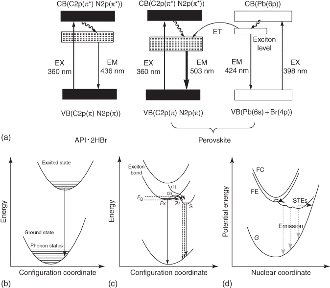
Figure 1.3.4 Proposed mechanisms for white emission in 2D‐OIHPs include (a) energy transfer mechanism, (b) deep‐level defect emission, and (c, d) self‐trapped excitons.
Source: Mechanism (a) is adapted with permission from ref. [20], copyright 2006 ACS. Mechanisms (b) and (c) are adapted with permission from ref. [33], copyright 2015 ACS. Mechanism (d) is adapted with permission from ref. [32], copyright 2016, ACS.
1.3.3.1 Energy Transfer Mechanism
The energy transfer mechanism responsible for WLE in (C6H13N3)PbBr4 perovskite was investigated in detail by Li et al. [20]. In particular, the energy transfer takes place from the inorganic to organic layer (Figure 1.3.4a). This conclusion was derived from excitation‐wavelength‐dependent PL measurements of (C6H13N3)PbBr4 and its organic component (C6H11N3)·2HBr. Upon exciting both samples with 360 nm, (C6H13N3)PbBr4 was found to emit broadly, peaking at 424 and 503 nm, across the visible wavelength (Figure 1.3.5a(i)). On the contrary, the emission of (C6H11N3)·2HBr, peaking at 436 nm, is weaker (Figure 1.3.5a(ii)). Photoluminescence (PL) excitation spectra of (C6H13N3)PbBr4 perovskite measured at 503 nm revealed two states (peaks at 398 and 360 nm) associated with its emission (Figure 1.3.5a(iii)). The former is due to the excitonic state in the inorganic layers, while the latter is due to the contribution from the organic layers (Figure 1.3.5a(iv)). This suggests that the organic layers play a role in the broad emission. Furthermore, upon exciting the samples with 398 nm, the emission of (C6H11N3)·2HBr quenches significantly, while the broad emission of (C6H13N3)PbBr4 remains invariant (Figure 1.3.5b). This suggests the presence of an energy transfer process from inorganic to organic layers in (C6H13N3)PbBr4, which is responsible for the broad emission. In addition, this suggests that direct excitation of the organic framework is not a prerequisite for the broad emission in (C6H13N3)PbBr4. A similar energy transfer process from inorganic to organic layers leading to a triplet emission has also been observed in naphthalene‐based 2D perovskite [48].
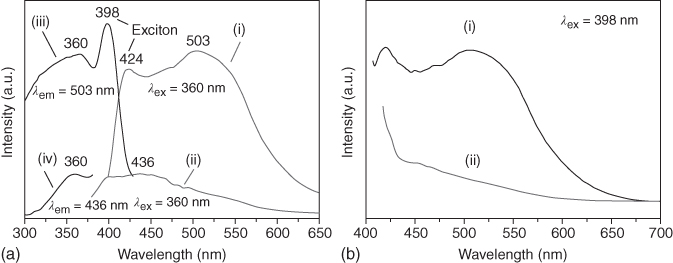
Figure 1.3.5 Broadband emission from an optically active organic component in (C6H13N3)PbBr4 perovskite. (a) PL emission (i and ii) and excitation (iii and iv) spectra for (C6H11N3)·2HBr (i, ii) and the perovskite compound 1 (iii, iv) under the same instrumental conditions. An excitation wavelength of 360 nm is used for PL emission measurements. (b) PL emission spectrum of perovskite (i) (C6H13N3)PbBr4, and (ii) (C6H11N3)·2HBr excited at 398 nm.
Source: Li et al. 2006 [20]. Copyright 2006. Adapted with permission of American Chemical Society.
1.3.3.2 Broadband Defect Emission
Defect‐related broadband emission could also be another origin for WLE in 2D perovskites. The intensity and profile of such emission are typically very dependent on defect concentrations. At higher excitation intensity, these defects become filled by the photoexcited charge carriers and emission intensity is expected to saturate. In addition, the emission profile should also show a strong dependence on particle size [49]. These signatures of defect‐related emission have not been observed in several white‐emitting 2D perovskite. Dohner et al. [31] have shown that the PL intensity of (EDBE)PbBr4 is linear, without saturation, with excitation intensity (Figure 1.3.6a). This linear behavior has also been observed in (C6H11NH3)2PbBr4 by Yangui et al. [33] (Figure 1.3.6b). In addition, the particle size of these perovskites has also been shown to have little influence on the broadband emission, with identical PL spectra reported for ball‐milled powder and single‐crystal samples [31, 44] (Figure 1.3.6c,d). These evidence suggest that defects in 2D‐OIHPs are unlikely to be the origin of the broadband emission. This is in contrast to 3D‐CH3NH3PbBr3 nanoclusters [46], where saturation of broadband PL emission (trap‐state‐related emission) is observed at higher laser fluences.
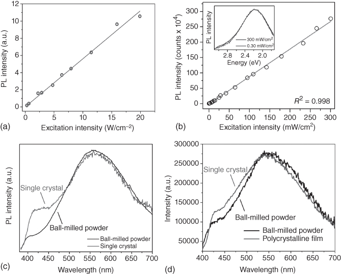
Figure 1.3.6 Non‐trap‐related broadband emission. A plot of PL intensity with excitation intensity of (a) (EDBE)PbBr4 and (b) (C6H11NH3)2PbBr4, showing a linear relationship without saturation. Comparison of PL spectrum between ball‐milled powder and a single crystal of (c) (EDBE)PbBr4 and (d) (N‐MEDA)PbBr4.
Source: (a) and (c) are adapted with permission from ref. [31], copyright 2014 ACS. (b) is adapted with permission from ref. [33], copyright 2015 ACS. (d) is adapted with permission from ref. [44], copyright 2014 ACS.
1.3.3.3 Self‐trapped Excitons
The presence of self‐trapped excitons (STEs) in white‐emitting 2D‐OIHPs were confirmed by Karunadasa and coworkers [31, 32]. There are four pieces of evidence suggesting the presence of STEs in these materials. The first evidence is the large exciton–phonon coupling strength (Γphonon) in (EDBE)PbBr4. A large Γphonon value increases the probability of STE formation [50]. A value of Γphonon = 130 ± 7 meV has been extracted from the temperature‐dependent full‐width at half maximum (FWHM) plot of (EDBE)PbBr4 (Figure 1.3.7a) via fitting using the expression:

Figure 1.3.7 Evidence of self‐trapped excitons. (a) Temperature dependence of the main emission bandwidth in (EDBE)PbBr4 and a fit to a model that includes contributions from vibronic coupling and inhomogeneous broadening due to defect sites. A large exciton–phonon coupling of 130 ± 7 meV was obtained from the fitting. (b) Intensity ratio of STE and free exciton luminescence (I STE/I FE) in (N‐MEDA)PbBr4 as a function of temperature under 343 nm photoexcitation. (c) Two‐dimensional pseudocolor (−ΔT/T o) plot of the TA spectrum as a function of probe wavelength and pump–probe delay for (N‐MEDA)PbBr4. (d) Normalized TA onsets probed at below‐gap wavelengths under 387 nm resonant photoexcitation at room temperature for (N‐MEDA)PbBr4.
Source: (a) is adapted with permission from ref. [31], copyright 2014 ACS. (b), (c) and (d) are adapted with permission from ref. [32], copyright 2016 ACS.
where Γ0 is the emission FWHM at T = 0 K, E LO is the energy of the longitudinal optical phonon mode energy, E b is the average binding energy of emissive defect states and Γphonon and Γinhomo are the electron–phonon coupling and inhomogeneous broadening constant. The fitted value of Γphonon is also comparable to ZnO multi‐quantum well systems [51], which are known for their large exciton–phonon coupling strength. The fitting also yields a value of E LO = 12 ± 1 meV, which corresponds well to the stretching frequency of PbBr bond and suggests self‐trapping of excitons at the inorganic framework.
The second evidence is the presence of a self‐trapping barrier. Its presence in (N‐MEDA)PbBr4 can be derived from Figure 1.3.7b where the PL intensity ratio of STE ( I STE ) and free excitons ( I FE ) decreases with temperature. This trend can be interpreted as due to an increased thermally driven back transfer of STE to the free exciton states at higher temperature, which leads to smaller I STE/I FE ratio at higher temperature. The presence of such a barrier has also been observed in (C6H11NH3)2PbBr4 broadband emitting system [33]. The third evidence can be seen from the presence of a photo‐induced absorption signal, i.e. lack of photo‐bleaching signal, in the transient absorption spectrum (Figure 1.3.7c,d) in (N‐MEDA)PbBr4. Since STEs are formed from free exciton trapping, optical transition from ground state to STE state should occur with a very low probability. This results in an absence of a photo‐bleaching signal at the visible wavelength, consistent with Figure 1.3.7c. This is evident from the good correspondence between the transient absorption rise time of ∼400 fs (Figure 1.3.7d) and period of PbBr stretching mode of ∼300 fs. These are characteristic signatures of STEs being the underlying mechanism for broadband emission in 2D‐OIHPs.
1.3.3.4 Role of Organic Framework in Broadband 2D‐OIHP Emitters
Self‐trapping at the inorganic framework has been widely assigned to the origins of broad emission in 2D‐OIHPs. However, the influence of the organic framework on white emission cannot be ruled out given the close proximity between the organic and inorganic layers. To date, studies have found that the organic framework plays two roles for white emission. Firstly, excitons generated in the inorganic halide layers can also undergo self‐trapping at the organic framework. The direct contribution of the organic framework to white emission has been demonstrated experimentally in (C6H5C2H4NH3)2PbCl4 2D‐OIHPs ([52]. A similar temperature‐dependent PL FWHM analysis was carried out using Eq. 1.3.1) and the fitting revealed ΓLO and E LO to be 265 ± 80 meV and 54 ± 6 meV, respectively. The large value of ΓLO is indicative of strong exciton–phonon coupling and suggests the presence of self‐trapped excitons. The value of E LO is also in good agreement with a phonon mode in C6H5C2H4NH3Cl. These evidence suggest the self‐trapping of excitons at the organic framework. Secondly, there is another report suggesting an alternative role of the organic cation–inorganic cage interaction in broadband emission. Specifically, certain organic cations could lead to a stronger lead halide bond distortion [53]. The distorted inorganic cage could, therefore, give rise to charge self‐trapping, resulting in broad emission from the inorganic framework.
Despite the different roles of the organic framework for the broadband emitter, both reports convey one important message: the organic framework is equally important as the inorganic framework for broadband emission. As such, these findings highlight that judicious selection of both organic and inorganic components presents new opportunities for tuning white emission from 2D‐OIHP.
1.3.4 Strong Exciton–Photon Coupling in 2D‐OIHPs
The large exciton oscillator strength and binding energy in 2D‐OIHPs also give rise to strong exciton–photon coupling. This strong interaction offers us new opportunities to unlock new physics and applications. In fact, fundamental studies of strong exciton–photon coupling in other semiconductor systems have been an active research area for decades. This quest for novel technologies was first pioneered by inorganics and then extended to organics. Promising results have been achieved for both systems, e.g. realization of a new type of coherent light source called as polariton lasers [54–62], each with its own advantages and drawbacks. Organic–inorganic hybrid halide perovskites, which possesses the best of both systems (i.e. excellent electrical and optical properties of inorganic system, with the low‐cost, chemical flexibility and versatility of organic system) are therefore exciting new systems to further explore these possibilities. However, these systems have only been recently investigated and just been realized in the UV bandgap 3D lead halide perovskite system [63], but are yet to be demonstrated for the 2D system with stronger excitonic behavior and visible emission. In this section, the early works on investigating the fundamentals of strong exciton–photon coupling in 2D perovskites systems are reviewed.
1.3.4.1 Jaynes–Cummings Model
One of the simplest theoretical models to describe the exciton–photon coupling phenomenon is the Jaynes–Cummings model. This model assumes a two‐level exciton/atom with ground state |a〉 and excited state |b〉 with energy E b − E a = ℏω 0 > 0 in the presence of a single‐mode radiation field with energy ℏω . Given the total energy of the system E = E a + (n + 1)ℏω , by conservation of energy there are only two possible quantum states available for the system: |a, n + 1〉 (i.e. ground state |a〉 with (n + 1) photons) and |b, n〉 (i.e. excited state |b〉 with n photon). These states are known as bare states, which do not include the interaction energy. The total Hamiltonian with interaction is given by
The third term corresponds to the interaction between the photon and exciton, which includes absorption and stimulated emission. Here, ![]() and
and ![]() are the creation and annihilation operators of the photon, respectively, (i.e.
are the creation and annihilation operators of the photon, respectively, (i.e. ![]() and
and ![]() );
ω
R
is the vacuum Rabi frequency, which parameterizes the coupling strength between the exciton/atom and photon; and
E
a
= − ℏω
0/2 and
E
b
= + ℏω
0/2 are taken as the energy reference. Note that the spontaneous emission term is omitted, which is valid when the spontaneous emission rate Γ is much slower than the field oscillation frequency ω (i.e. Γ ≪ ω). For algebraic simplification, the Rabi energy
);
ω
R
is the vacuum Rabi frequency, which parameterizes the coupling strength between the exciton/atom and photon; and
E
a
= − ℏω
0/2 and
E
b
= + ℏω
0/2 are taken as the energy reference. Note that the spontaneous emission term is omitted, which is valid when the spontaneous emission rate Γ is much slower than the field oscillation frequency ω (i.e. Γ ≪ ω). For algebraic simplification, the Rabi energy ![]() and detuning energy Δ = ℏω
0 − ℏω
are defined. The eigenstates of this Hamiltonian in (Eq. 1.3.2) is given by
and detuning energy Δ = ℏω
0 − ℏω
are defined. The eigenstates of this Hamiltonian in (Eq. 1.3.2) is given by
where
The eigenenergies of the above eigenstates are
It is clear that the eigenenergies are no longer pure photon states or excited exciton/atom states, but are a quantum mixture of both, which is termed as photon‐dressed states. In the case of the exciton, it is also known as exciton–polariton. The signature of this interaction is the energy shift from the bare states and the anti‐crossing of the eigenenergies at zero detuning – see Figure 1.3.8.
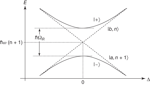
Figure 1.3.8 The eigenenergies of the dressed states as a function of detuning Δ. The eigenenergies show anti‐crossing behavior, as compared to crossing behavior of the non‐interacting bare states.
1.3.4.2 Exciton–Photon Coupling in 2D Perovskites Thin Films: Optical Stark Effect
From the Jaynes–Cummings model, strong exciton–photon coupling results in the shift of the energy as compared to the bare states. When the frequency of a light pulse is red‐detuned with respect to the excitonic resonance (Δ > 0), the eigenenergy of the system (i.e. absorption) will be blueshifted as much as
which is the shift from |b, n〉 to |+〉. This effect is also known as the optical Stark effect (OSE). It is a useful phenomenon to investigate the strength of light‐matter coupling in a material system. Recently, T.C. Sum and coworkers reported a study of strong exciton–photon coupling in several solution‐processed 2D perovskite thin films via OSE: (C6H5C2H4NH3)2PbBr4, (C6H5C2H4NH3)2PbI4, and (C6H4FC2H4NH3)2PbI4 (called PEPB, PEPI, and FPEPI, respectively) [64]. In these films, ultrafast spin‐selective OSE was observed at room temperature using transient absorption spectroscopy (TAS). The illustrated and the experimental spectral OSE signature from TAS is shown in Figure 1.3.9a,b, respectively, from which the energy shift can be estimated. Furthermore, Figure 1.3.9b,c shows the spin selectivity of this process, represented by the dependence on the pump and probe circular polarization. The OSE spectral signature can only be observed when the pump and probe are co‐circular during the duration of the pump. Meanwhile, the counter‐circular pump and probe polarization results in a state‐filling TA signal, which arises from two‐photon absorption. This is confirmed by the linear and quadratic behavior of the co‐circular and counter‐circular signal, respectively – Figure 1.3.9d. This study uncovers an energy shift of ∼4.5 meV on PEPI thin film with linear absorption spectrum peaked at ∼2.39 eV, by pump laser with photon energy of 2.16 eV and fluence of 1.66 mJ cm−2.

Figure 1.3.9 (a) The illustration of OSE and its spectral signature. The circular polarization dependence (b) spectral, and (c) temporal signature of OSE signal. (d) Linear behavior of the estimated energy shift from OSE with respect to pump fluence. The signal from counter‐circular polarization shows a quadratic behavior, consistent with a two‐photon absorption process. (e) The normalized Rabi energy shows a direct correspondence to the dielectric contrast of the organic and inorganic layer, but not to the oscillator strength.
Source: Giovanni et al. 2016 [64]. Adapted with permission of AAAS.
From the energy shift, Rabi energy ℏΩR of ∼33 meV, ∼47 meV and ∼63 meV were estimated under such pump fluence on PEPB, PEPI, and FPEPI thin films, respectively. The Rabi energy by these 2D perovskites system at room temperature was found to be about four times higher than that for a classic inorganic semiconductor system GaAs/AlGaAs multi‐quantum well (MQW) at cryogenic temperature excited under similar pump fluence. This result is also consistent with other studies, which had found the vacuum Rabi energy of PEPI (in a cavity) to be one order of magnitude higher than GaAs‐based cavity system [65–67] (this will be discussed later). While one reason could be the higher oscillator strength of the 2D perovskites as compared to GaAs [65–67], this recent work (Ref. [64]) surprisingly revealed that it is the strength of Rabi energy normalized with respect to square root of fluence (and thus fluence independent) that is proportional to the dielectric contrast of the organic and inorganic layers, rather than simply due to the oscillator strength (see Figure 1.3.9e). Although this result provides a pragmatic straightforward strategy for tuning the exciton–photon coupling strength in 2D perovskites material system, further studies are warranted to clearly understand these dependencies.
1.3.4.3 Exciton–Photon Coupling in 2D Perovskite Microcavities: Exciton–Polariton
As described by the Jaynes–Cummings model, the strong interaction between the exciton and the photon will result in new eigenstates which are admixtures of both the exciton and the photon states. This interaction is parameterized by the vacuum Rabi frequency ω R :
where ![]() is the transition dipole moment of the exciton, and
V
m
is the photon confinement volume. From the abovementioned relation, optical confinement of the system (e.g. by using optical cavity) will strongly reduce
V
m
and thus enhance the exciton–photon coupling strength. In this so‐called strong coupling regime, the new eigenstates form a new quasi‐particle with a distinct anti‐crossing dispersion relation, known as the exciton–polariton. The main proof of the presence of this strong coupling regime is the anti‐crossing between the new eigenenergies, typically called the
upper polariton branch
(UPB) and
lower polariton branch
(LPB). Exciton–polariton exhibits many exotic physical phenomena such as Bose–Einstein condensation (BEC). BEC is basically the macroscopic occupation of the polariton ground state. The ability to condense and manipulate these exciton–polaritons will lead to new technologies that include polariton lasers, optical‐spin switches for transistors and IC [68–72], logic gates [70, 71], etc.
is the transition dipole moment of the exciton, and
V
m
is the photon confinement volume. From the abovementioned relation, optical confinement of the system (e.g. by using optical cavity) will strongly reduce
V
m
and thus enhance the exciton–photon coupling strength. In this so‐called strong coupling regime, the new eigenstates form a new quasi‐particle with a distinct anti‐crossing dispersion relation, known as the exciton–polariton. The main proof of the presence of this strong coupling regime is the anti‐crossing between the new eigenenergies, typically called the
upper polariton branch
(UPB) and
lower polariton branch
(LPB). Exciton–polariton exhibits many exotic physical phenomena such as Bose–Einstein condensation (BEC). BEC is basically the macroscopic occupation of the polariton ground state. The ability to condense and manipulate these exciton–polaritons will lead to new technologies that include polariton lasers, optical‐spin switches for transistors and IC [68–72], logic gates [70, 71], etc.
To achieve BEC, these exciton–polaritons should thermalize to the ground state. However, this thermalization process is nontrivial. The early stage involves the relaxation via acoustic phonons from the higher states toward the inflection point of the LPB (i.e. around the anti‐crossing point between LPB and UPB). Nonetheless, beyond the inflection point, the LPB dispersion becomes too steep for any relaxation via scattering with acoustic phonons. This results in a significant slowing of the polariton relaxation to the ground state, known as the polariton bottleneck effect, which is a major challenge toward achieving BEC [60, 62]. One proposed approach to achieve BEC is through a parametric scattering of the exciton–polaritons, where two exciton–polaritons scatter with each other, resulting in one polariton in the ground state and the other at a higher energy state, conserving total energy and momentum in the process. Due to the bosonic properties of exciton–polaritons, a small population in the ground state will stimulate more parametric scattering events to occur. This process is known as stimulated scattering. Another mechanism which has also been suggested to enhance polariton relaxation is via polariton‐free carrier scattering [73, 74].
The investigation of the presence of strong coupling regime in 2D perovskites was pioneered by Ishihara and coworkers [65]. The experiment was performed on a patterned quartz substrate coated with PEPI, forming a distributed feedback (DFB) cavity at room temperature. The polaritonic behavior in the strong coupling regime of this system was evident from the observed anti‐crossing behavior of the dips position as a function of the grating periodicities (photon mode detuning) from the absorption spectra. This anti‐crossing energy splitting (also known as Rabi splitting) was found to be ∼100 meV in room temperature, which is much higher than the ∼9 meV splitting in the GaAs system. Another evidence of the strong coupling in this system is from the energy‐momentum dispersion relation in the system, which could be investigated using the angle‐resolved transmissivity measurements (i.e. by changing photon incident angle, hence changing photon momentum projection on sample plane). The observed anti‐crossing behavior in momentum space validated the presence of exciton–polariton in this simple system. However, there was no discussion on achieving BEC in this work.
Following Ishihara's pioneering study, the work on exciton–polaritons in 2D perovskite cavity was further advanced mainly by Deleporte and coworkers, which focused on PEPI in Fabry–Perot (FP) cavity architecture at room temperature [34, 36, 66, 67, 75–77]. In the FP cavity, light is confined in one direction (taken as z‐axis), which forms a standing wave. Depending on the thickness, the cavity photon acquires a minimum standing wave energy of E 0 = hc ′/mλ 0 , where m = 1, 2, 3, …; c ′ = c/n eff is the speed of light in the microcavity with n eff as the effective refractive index; and λ 0 = n eff d/2 is the minimum standing wave wavelength allowed with d as cavity thickness. The cavity photon momentum wave vector k is defined along the x–y plane. The energy dispersion of the FP cavity is therefore given by
where
E
x
is the exciton energy; and ![]() is the momentum‐dependent energy of the cavity photon.
is the momentum‐dependent energy of the cavity photon.
Figure 1.3.10a shows the typical FP cavity system containing 2D perovskites. The fabrication of such cavity includes spin coating the 2D perovskite precursor solution as the active material, spin coating of the PMMA layer as the spacer, and, lastly, evaporation of silver as the top reflector layer. In this type of cavity, depending on the refractive index, the thickness of each material layer can be adjusted to maximize the light electric field “experienced” by the active material. Figure 1.3.10b shows the simulated electric field intensity distribution in one such example of the 2D perovskite FP cavity architecture, where the perovskite layer is designed to yield the maximum intensity and hence strengthen the interaction. The tuning of layer thickness in this architecture also allows the relative detuning between the 2D perovskite exciton mode and the cavity mode [67]. The exciton–polariton dispersion relation in the FP cavity can then be inferred from the angle‐resolved reflectivity measurement (Figure 1.3.10c), where the dips in the reflectivity spectra indicate the energy dispersion of the polariton states. Figure 1.3.10d shows the plot of energy dips as a function of the angle. A clear anti‐crossing behavior with Rabi splitting in order of 100 meV is observed, which indicates the presence of a strong coupling regime in this cavity system. Anti‐crossing behavior and Rabi splitting with a similar order of magnitude are also found in FPEPI‐based FP cavity [36].

Figure 1.3.10 (a) Fabry–Perot cavity system employing 2D perovskites as the active material. (b) Angle‐resolved reflectivity measurements on the cavity showing dips which correspond to the UPB and the LPB. (c) Theoretical simulation on the light field intensity inside the cavity. (d) A plot of UPB and LPB dispersion of the 2D perovskite FP cavity.
Source: This figure is adapted with permission from ref. [67], copyright 2016 IOP Publishing.
However, regardless of the presence of the strong coupling regime, the observation of BEC in 2D perovskites cavity remains elusive. While emission from the LPB has been observed, the polariton bottleneck effect was found to be the major challenge for realizing BEC in the 2D perovskite cavity, signified by strong emission at large angle [36, 67]. Another factor which contributes to the problem is the relatively low‐quality FP cavity fabricated using such solution‐processed and metal evaporation techniques. The fabricated FP cavity only has a Q‐factor of ∼25 [66], much lower than typical high‐quality cavity system with Q‐factor ≥ 1000. Another attempt to improve the Q‐factor was also performed by Deleporte and coworkers, using separate growth of the distributed Bragg reflectors (DBR) and the assembly technique based on the liquid migration on the top of the dielectric mirror [34]. This microcavity architecture is depicted in Figure 1.3.11a. The top DBR, which consisted of eight pairs of YF3/ZnS λ/4‐layers with stop‐band centered at PEPI PL peak (2.37 eV), was first evaporated at low temperature (<100 °C) on a Si substrate coated with a polymer sacrificial layer with thin Ti/Ni top bilayer as compensator for the internal stress of the multilayer pile. Meanwhile, the bottom DBR (stop‐band centered at 2.37 eV), which consisted of 11 pairs of SiN x /SiO2 λ/4‐layers, were deposited on a fused silica substrate by plasma‐enhanced chemical vapor deposition. The PEPI layer with a thickness of ∼60 nm was then spin coated on top of the bottom DBR, continued by sputtering SiN x layer, which acts as a spacer. The top DBR was then immersed in a solvent which dissolved the sacrificial polymer layer, which therefore released it from the Si substrate. By gradually exchanging the initial solvent with toluene (does not dissolve PEPI), the released top DBR floated on toluene, which was then positioned onto the designated substrate of SiN x /perovskites/bottom DBR. The toluene solution was then gradually evacuated and annealed at 90 °C. This results in the adsorption of the top DBR by the surface of the SiN x layer via van der Waals force with a good mechanical contact.

Figure 1.3.11 (a) Fabrication technique of the high‐Q planar cavity. (b) Reflectivity spectra at normal incidence. (c) Emission of high Q‐factor 2D perovskite‐based cavity.
Source: Han et al. 2012 [34]. Copyright 2012.Adapted with permission of The Optical Society.
From the reflectivity spectrum, three polariton branches, labeled as LPB, MPB, and HPB (correspond to low, middle, and high polariton branch, respectively) were observed in the cavity (Figure 1.3.11b), which arose from the coupling of the perovskite exciton to both the cavity mode and the Bragg mode just at the lower energy edge of the SiO2/SiN x DBR stop‐band. Meanwhile, the emission spectra exhibit well‐resolved polariton branches without any significant emission from the uncoupled perovskite exciton (contrary to previously reported low Q‐factor samples [36, 67, 76]). Efficient polariton relaxation toward the bottom of the MPB was also observed. The Q‐factor of the DBR is 86, which was an improvement by a factor of >3 from the previous metal‐based top mirror layer (Figure 1.3.11c). However, room temperature BEC 2D perovskite remained elusive.
More recently, there was another report by Deleporte's group for the PEPI perovskite system embedded in the FP cavity made by similar migration in liquid technique [77]. In this latest study, the measurement was performed on a ∼900‐nm‐diameter sphere‐like defect site, which provides extra zero dimension (0D)‐like confinement on the perovskite system. The strong coupling regime in such system was marked by observations of the discrete PL of the LPB. While the polariton bottleneck issue has yet been tackled, the measured emission Q‐factor was ∼750, which was almost an order of magnitude improvement over the previous system. This work demonstrated the feasibility of further improvements for realizing room temperature BEC with the 2D‐OIHP system.
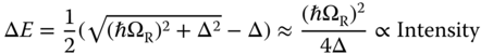
Strong coupling is not limited to occurrences between the exciton and photon. More recently, Niu et al. [78] reported observations of strong interaction between photons, excitons, and surface plasmons in Ag‐based DFB grating coated with 2D perovskite (C6H9C2H4NH3)2PbI4 (or CHPI), with coupling strengths that are one order larger than for III–V quantum wells at room temperature (Figure 1.3.12a). This study was mainly done by incident polar (θ) and azimuthal (ϕ) angle‐resolved reflectivity measurement with transverse electric (TE) and transverse magnetic (TM) modes. Under TM mode excitation (Figure 1.3.12b), the presence of an additional ∼100 meV redshifted exciton dip was observed, which was assigned to the excitation of the surface plasmon polariton (SPP). This effect was absent in TE mode measurements (Figure 1.3.12c) and CHPI‐coated planar Ag‐film (Figure 1.3.12d). This redshift of ∼100 meV could be well explained by the method of images, where the exciton in CHPI coupled via Coulomb interaction with its own image on the metal surface, forming a “biexciton.” The magnitude of the redshift observed agrees very well with the well‐established model in Ref. [79]. Further tunability of this “biexciton” redshift was also demonstrated up to 185 meV by simply changing the azimuthal angle of the incident light. This “biexciton” holds an interesting potential application for light‐emission devices, since its decay channel via emission to SPP (Figure 1.3.12e) has been previously used to improve the luminescence efficiency of LEDs [80, 81]. The strong interaction of the exciton, bi‐exciton, and the grating mode could be well explained using the three coupled‐oscillators model (Figure 1.3.12f), where large Rabi splitting of 156 and 125 meV were obtained for the exciton and biexciton interaction with SPP, respectively. These values are comparable to those with J‐aggregates. These results, therefore, open up an exciting new direction for optoelectronic applications through coupling SPP with exciton–photon interaction in 2D perovskites.
Figure 1.3.12 (a) CHPI/Ag‐based DFB grating, which is the system under study in Ref. [78]. Angle‐resolved reflectivity spectra of the sample with (b) TM (c) TE, and (d) planar mode measurements. The arrows indicate the observed exciton mode. (e) A schematic mechanism for SPP‐mediated emission of the image biexciton. (f) Extracted spectral mode positions reflection dips (open circles) with ϕ = 90°, fitted with three coupled‐oscillators model (dashed lines).
Source: Niu et al. 2015 [78]. Copyright 2015. Adapted with permission of American Physical Society.
1.3.5 Concluding Remarks
In conclusion, 2D‐OIHPs possess novel electronic properties, akin to their 3D counterparts. Quantum and dielectric confinement effect in 2D‐OIHPs strongly enhanced its excitonic binding energy and oscillator strength, hence endowing it with great potential for exciton‐based applications. 2D‐OIHPs are especially interesting due to their much stronger interactions with phonons and photons compared to other conventional systems. In this chapter, we highlighted some of the most recent studies which aimed to uncover the fundamental understanding and implications of these strong interactions. While there has been some success in qualitative modeling to partially explain experimental observations on the phenomenological level, the detailed photophysical mechanisms and origins of the strong interaction are still not fully understood. Furthermore, issues such as lower mobility than traditional semiconductors, polariton bottleneck, etc. remain unresolved. Importantly, the holy grail of achieving BEC with these 2D perovskite systems remains elusive. Most recently, another family of perovskites known as Ruddlesden–Popper (RP) perovskites, possessing self‐assembled MQW structure similar to 2D perovskites but with tunable well thickness, has entered the field. Due to their better ambient moisture resilience as compared to 3D and relatively strong excitonic properties [13], efficient LEDs [6] and photovoltaic devices [13] have been demonstrated using this novel system. Further research into understanding these interactions is key to the realization of applications of white‐light LEDs, polariton lasers, or plasmonic devices based on 2D OIHPs. The future of perovskite LEDs continues to shine brightly.
References
- 1 Saliba, M., Matsui, T., Seo, J.‐Y. et al. (2016). Cesium‐containing triple cation perovskite solar cells: improved stability, reproducibility and high efficiency. Energy Environ. Sci. 9 (6): 1989–1997.
- 2 Bi, D., Tress, W., Dar, M.I. et al. (2016). Efficient luminescent solar cells based on tailored mixed‐cation perovskites. Sci. Adv. 2 (1): e1501170.
- 3 NREL: Efficiency Chart (2017). Best research‐cell efficiencies. https://www.nrel.gov/pv/assets/images/efficiency‐chart.png (accessed 10 September 2017).
- 4 Tan, Z.‐K., Moghaddam, R.S., Lai, M.L. et al. (2014). Bright light‐emitting diodes based on organometal halide perovskite. Nat. Nanotechnol. 9 (9): 687–692.
- 5 Cho, H., Jeong, S.‐H., Park, M.‐H. et al. (2015). Overcoming the electroluminescence efficiency limitations of perovskite light‐emitting diodes. Science 350 (6265): 1222–1225.
- 6 Yuan, M., Quan, L.N., Comin, R. et al. (2016). Perovskite energy funnels for efficient light‐emitting diodes. Nat. Nanotechnol. 11 (10): 872–877.
- 7 Xing, G., Mathews, N., Lim, S.S. et al. (2014). Low‐temperature solution‐processed wavelength‐tunable perovskites for lasing. Nat. Mater. 13 (5): 476–480.
- 8 Zhu, H., Fu, Y., Meng, F. et al. (2015). Lead halide perovskite nanowire lasers with low lasing thresholds and high quality factors. Nat. Mater. 14 (6): 636–642.
- 9 Yakunin, S., Protesescu, L., Krieg, F. et al. (2015). Low‐threshold amplified spontaneous emission and lasing from colloidal nanocrystals of caesium lead halide perovskites. Nat. Commun. 6: 8056.
- 10 Dou, L., Yang, Y., You, J. et al. (2014). Solution‐processed hybrid perovskite photodetectors with high detectivity. Nat. Commun. 5: 5404.
- 11 Fang, Y., Dong, Q., Shao, Y. et al. (2015). Highly narrowband perovskite single‐crystal photodetectors enabled by surface‐charge recombination. Nat. Photonics 9 (10): 679–686.
- 12 Chin, X.Y., Cortecchia, D., Yin, J. et al. (2015). Lead iodide perovskite light‐emitting field‐effect transistor. Nat. Commun. 6: 7383.
- 13 Tsai, H., Nie, W., Blancon, J.‐C. et al. (2016). High‐efficiency two‐dimensional Ruddlesden–Popper perovskite solar cells. Nature 536 (7616): 312–316.
- 14 Koutselas, I., Bampoulis, P., Maratou, E. et al. (2011). Some unconventional organic−inorganic hybrid low‐dimensional semiconductors and related light‐emitting devices. J. Phys. Chem. C 115 (17): 8475–8483.
- 15 Ahmad, S., Kanaujia, P.K., Beeson, H.J. et al. (2015). Strong photocurrent from two‐dimensional excitons in solution‐processed stacked perovskite semiconductor sheets. ACS Appl. Mater. Interfaces 7 (45): 25227–25236.
- 16 Kawamura, Y., Mashiyama, H., and Hasebe, K. (2002). Structural study on cubic–tetragonal transition of CH3NH3PbI3. J. Phys. Soc. Jpn. 71 (7): 1694–1697.
- 17 Papavassiliou, G.C. (1997). Three‐ and low‐dimensional inorganic semiconductors. Prog. Solid State Chem. 25 (3): 125–270.
- 18 Sum, T.C. and Mathews, N. (2014). Advancements in perovskite solar cells: photophysics behind the photovoltaics. Energy Environ. Sci. 7 (8): 2518–2534.
- 19 Umebayashi, T., Asai, K., Kondo, T., and Nakao, A. (2003). Electronic structures of lead iodide based low‐dimensional crystals. Phys. Rev. B 67 (15): 155405.
- 20 Li, Y.Y., Lin, C.K., Zheng, G.L. et al. (2006). Novel 〈110〉‐oriented organic−inorganic perovskite compound stabilized by N‐(3‐aminopropyl)imidazole with improved optical properties. Chem. Mater. 18 (15): 3463–3469.
- 21 Pradeesh, K., Nageswara Rao, K., and Vijaya Prakash, G. (2013). Synthesis, structural, thermal and optical studies of inorganic–organic hybrid semiconductors, R‐PbI4. J. Appl. Phys. 113 (8): 083523.
- 22 Ahmad, S., Hanmandlu, C., Kanaujia, P.K., and Prakash, G.V. (2014). Direct deposition strategy for highly ordered inorganic organic perovskite thin films and their optoelectronic applications. Opt. Mater. Express 4 (7): 1313–1323.
- 23 Dang, Y., Ju, D., Wang, L., and Tao, X. (2016). Recent progress in the synthesis of hybrid halide perovskite single crystals. CrystEngComm 18 (24): 4476–4484.
- 24 Yuan, Z., Shu, Y., Tian, Y. et al. (2015). A facile one‐pot synthesis of deep blue luminescent lead bromide perovskite microdisks. Chem. Commun. 51 (91): 16385–16388.
- 25 Niu, W., Eiden, A., Vijaya Prakash, G., and Baumberg, J.J. (2014). Exfoliation of self‐assembled 2D organic–inorganic perovskite semiconductors. Appl. Phys. Lett. 104 (17): 171111.
- 26 Mitzi, D.B., Prikas, M.T., and Chondroudis, K. (1999). Thin film deposition of organic−inorganic hybrid materials using a single source thermal ablation technique. Chem. Mater. 11 (3): 542–544.
- 27 Era, M., Hattori, T., Taira, T., and Tsutsui, T. (1997). Self‐organized growth of PbI‐based layered perovskite quantum well by dual‐source vapor deposition. Chem. Mater. 9 (1): 8–10.
- 28 Cheng, Z. and Lin, J. (2010). Layered organic–inorganic hybrid perovskites: structure, optical properties, film preparation, patterning and templating engineering. CrystEngComm 12 (10): 2646–2662.
- 29 Cao, D.H., Stoumpos, C.C., Farha, O.K. et al. (2015). 2D homologous perovskites as light‐absorbing materials for solar cell applications. J. Am. Chem. Soc. 137 (24): 7843–7850.
- 30 Smith, I.C., Hoke, E.T., Solis‐Ibarra, D. et al. (2014). A layered hybrid perovskite solar‐cell absorber with enhanced moisture stability. Angew. Chem. Int. Ed. 53 (42): 11232–11235.
- 31 Dohner, E.R., Jaffe, A., Bradshaw, L.R., and Karunadasa, H.I. (2014). Intrinsic white‐light emission from layered hybrid perovskites. J. Am. Chem. Soc. 136 (38): 13154–13157.
- 32 Hu, T., Smith, M.D., Dohner, E.R. et al. (2016). Mechanism for broadband white‐light emission from two‐dimensional (110) hybrid perovskites. J. Phys. Chem. Lett. 7 (12): 2258–2263.
- 33 Yangui, A., Garrot, D., Lauret, J.S. et al. (2015). Optical investigation of broadband white‐light emission in self‐assembled organic–inorganic perovskite (C6H11NH3)2PbBr4. J. Phys. Chem. C 119 (41): 23638–23647.
- 34 Han, Z., Nguyen, H.‐S., Boitier, F. et al. (2012). High‐Q planar organic–inorganic perovskite‐based microcavity. Opt. Lett. 37 (24): 5061–5063.
- 35 Lanty, G., Zhang, S., Lauret, J.S. et al. (2011). Hybrid cavity polaritons in a ZnO‐perovskite microcavity. Phys. Rev. B 84 (19): 195449.
- 36 Wei, Y., Lauret, J.S., Galmiche, L. et al. (2012). Strong exciton–photon coupling in microcavities containing new fluorophenethylamine based perovskite compounds. Opt. Express 20 (9): 10399–10405.
- 37 Ishihara, T., Takahashi, J., and Goto, T. (1990). Optical properties due to electronic transitions in two‐dimensional semiconductors (C n H2n+1NH3)2PbI4. Phys. Rev. B 42 (17): 11099–11107.
- 38 Kitazawa, N., Aono, M., and Watanabe, Y. (2012). Temperature‐dependent time‐resolved photoluminescence of (C6H5C2H4NH3)2PbX4 (X = Br and I). Mater. Chem. Phys. 134 (2–3): 875–880.
- 39 Tanaka, K., Sano, F., Takahashi, T. et al. (2002). Two‐dimensional Wannier excitons in a layered‐perovskite‐type crystal (C6H13NH3)2PbI4. Solid State Commun. 122 (5): 249–252.
- 40 Papavassiliou, G.C. (1996). Synthetic three‐ and lower‐dimensional semiconductors based on inorganic units. Mol. Cryst. Liq. Cryst. Sci. Technol., Sect. A 286 (1): 231–238.
- 41 Ishihara, T., Hong, X., Ding, J., and Nurmikko, A.V. (1992). Dielectric confinement effect for exciton and biexciton states in PbI4‐based two‐dimensional semiconductor structures. Surf. Sci. 267 (1): 323–326.
- 42 Shimizu, M., Fujisawa, J.‐I., and Ishi‐Hayase, J. (2005). Influence of dielectric confinement on excitonic nonlinearity in inorganic–organic layered semiconductors. Phys. Rev. B 71 (20): 205306.
- 43 Zhang, S., Audebert, P., Wei, Y. et al. (2011). Synthesis and optical properties of novel organic‐inorganic hybrid UV (R‐NH3)2PbCl4 semiconductors. J. Mater. Chem. 21 (2): 466–474.
- 44 Dohner, E.R., Hoke, E.T., and Karunadasa, H.I. (2014). Self‐assembly of broadband white‐light emitters. J. Am. Chem. Soc. 136 (5): 1718–1721.
- 45 Yuan, Z., Zhou, C., Tian, Y. et al. (2017). One‐dimensional organic lead halide perovskites with efficient bluish white‐light emission. Nat. Commun. 8: 14051.
- 46 Teunis, M.B., Lawrence, K.N., Dutta, P. et al. (2016). Pure white‐light emitting ultrasmall organic–inorganic hybrid perovskite nanoclusters. Nanoscale 8 (40): 17433–17439.
- 47 Zhang, F., Zhong, H., Chen, C. et al. (2015). Brightly luminescent and color‐tunable colloidal CH3NH3PbX3 (X = Br, I, Cl) quantum dots: potential alternatives for display technology. ACS Nano 9 (4): 4533–4542.
- 48 Ema, K., Inomata, M., Kato, Y. et al. (2008). Nearly perfect triplet‐triplet energy transfer from Wannier excitons to naphthalene in organic–inorganic hybrid quantum‐well materials. Phys. Rev. Lett. 100 (25): 257401.
- 49 Bowers, M.J., McBride, J.R., and Rosenthal, S.J. (2005). White‐light emission from magic‐sized cadmium selenide nanocrystals. J. Am. Chem. Soc. 127 (44): 15378–15379.
- 50 Gardens, O.G. (2007). Trends in Optical Materials Research. Nova Publishers.
- 51 Makino, T., Segawa, Y., and Kawasaki, M. (2005). Analytical study on exciton‐longitudinal‐optical‐phonon coupling and comparison with experiment for ZnO quantum wells. J. Appl. Phys. 97 (10): 106111.
- 52 Thirumal, K., Chong, W.K., Xie, W. et al. (2017). Morphology‐independent stable white‐light emission from self‐assembled two‐dimensional perovskites driven by strong exciton–phonon coupling to the organic framework. Chem. Mater. 29 (9): 3947–3953.
- 53 Cortecchia, D., Neutzner, S., Srimath Kandada, A.R. et al. (2017). Broadband emission in two‐dimensional hybrid perovskites: the role of structural deformation. J. Am. Chem. Soc. 139 (1): 39–42.
- 54 Das, A., Bhattacharya, P., Heo, J. et al. (2013). Polariton Bose–Einstein condensate at room temperature in an Al(Ga)N nanowire–dielectric microcavity with a spatial potential trap. Proc. Natl. Acad. Sci. USA 110 (8): 2735–2740.
- 55 Kena Cohen, S. and Forrest, S.R. (2010). Room‐temperature polariton lasing in an organic single‐crystal microcavity. Nat. Photonics 4 (6): 371–375.
- 56 Kim, S., Zhang, B., Wang, Z. et al. (2016). Coherent polariton laser. Phys. Rev. X 6 (1): 011026.
- 57 Schneider, C., Rahimi‐Iman, A., Kim, N.Y. et al. (2013). An electrically pumped polariton laser. Nature 497 (7449): 348–352.
- 58 Deng, H., Weihs, G., Snoke, D. et al. (2003). Polariton lasing vs. photon lasing in a semiconductor microcavity. Proc. Natl. Acad. Sci. USA 100 (26): 15318–15323.
- 59 Kavokin, A., Malpuech, G., and Laussy, F.P. (2003). Polariton laser and polariton superfluidity in microcavities. Phys. Lett. A 306 (4): 187–199.
- 60 Byrnes, T., Kim, N.Y., and Yamamoto, Y. (2014). Exciton–polariton condensates. Nat. Phys. 10 (11): 803–813.
- 61 Deng, H., Weihs, G., Santori, C. et al. (2002). Condensation of semiconductor microcavity Exciton polaritons. Science 298 (5591): 199–202.
- 62 Kavokin, A. and Malpuech, G. (2003). Frequently asked questions. In: Thin Films and Nanostructures, vol. 32 (ed. K. Alexey and M. Guillaume), 13–26. Academic Press.
- 63 Su, R., Diederichs, C., Wang, J. et al. (2017). Room‐temperature polariton lasing in all‐inorganic perovskite nanoplatelets. Nano Lett. 17 (6): 3982–3988.
- 64 Giovanni, D., Chong, W.K., Dewi, H.A. et al. (2016). Tunable room‐temperature spin‐selective optical stark effect in solution‐processed layered halide perovskites. Sci. Adv. 2 (6): 1600477.
- 65 Fujita, T., Sato, Y., Kuitani, T., and Ishihara, T. (1998). Tunable polariton absorption of distributed feedback microcavities at room temperature. Phys. Rev. B 57 (19): 12428–12434.
- 66 Brehier, A., Parashkov, R., Lauret, J.S., and Deleporte, E. (2006). Strong exciton–photon coupling in a microcavity containing layered perovskite semiconductors. Appl. Phys. Lett. 89 (17): 171110.
- 67 Lanty, G., Bréhier, A., Parashkov, R. et al. (2008). Strong exciton–photon coupling at room temperature in microcavities containing two‐dimensional layered perovskite compounds. New J. Phys. 10 (6): 065007.
- 68 Li, G., Liew, T.C.H., Egorov, O.A., and Ostrovskaya, E.A. (2015). Incoherent excitation and switching of spin states in exciton–polariton condensates. Phys. Rev. B 92 (6): 064304.
- 69 Liew, T.C.H., Kavokin, A.V., Ostatnický, T. et al. (2010). Exciton–polariton integrated circuits. Phys. Rev. B 82 (3): 033302.
- 70 Ballarini, D., De Giorgi, M., Cancellieri, E. et al. (2013). All‐optical polariton transistor. Nat. Commun. 4: 1778.
- 71 Gao, T., Eldridge, P.S., Liew, T.C.H. et al. (2012). Polariton condensate transistor switch. Phys. Rev. B 85 (23): 235102.
- 72 Amo, A., Liew, T.C.H., Adrados, C. et al. (2010). Exciton–polariton spin switches. Nat. Photonics 4 (6): 361–366.
- 73 Tartakovskii, A.I., Krizhanovskii, D.N., Malpuech, G. et al. (2003). Giant enhancement of polariton relaxation in semiconductor microcavities by polariton‐free carrier interaction: experimental evidence and theory. Phys. Rev. B 67 (16): 165302.
- 74 Lagoudakis, P.G., Martin, M.D., Baumberg, J.J. et al. (2003). Electron–polariton scattering in semiconductor microcavities. Phys. Rev. Lett. 90 (20): 206401.
- 75 Wenus, J., Parashkov, R., Ceccarelli, S. et al. (2006). Hybrid organic–inorganic exciton–polaritons in a strongly coupled microcavity. Phys. Rev. B 74 (23): 235212.
- 76 Lanty, G., Lauret, J.S., Deleporte, E. et al. (2008). UV polaritonic emission from a perovskite‐based microcavity. Appl. Phys. Lett. 93 (8): 081101.
- 77 Nguyen, H.S., Han, Z., Abdel‐Baki, K. et al. (2014). Quantum confinement of zero‐dimensional hybrid organic–inorganic polaritons at room temperature. Appl. Phys. Lett. 104 (8): 081103.
- 78 Niu, W., Ibbotson, L.A., Leipold, D. et al. (2015). Image excitons and plasmon‐exciton strong coupling in two‐dimensional perovskite semiconductors. Phys. Rev. B 91 (16): 161303.
- 79 Chance, R.R., Prock, A., and Silbey, R. (1975). Frequency shifts of an electric‐dipole transition near a partially reflecting surface. Phys. Rev. A 12 (4): 1448–1452.
- 80 Frischeisen, J., Niu, Q., Abdellah, A. et al. (2011). Light extraction from surface plasmons and waveguide modes in an organic light‐emitting layer by nanoimprinted gratings. Opt. Express 19 (S1): A7–A19.
- 81 Kumar, A., Srivastava, R., Tyagi, P. et al. (2012). Efficiency enhancement of organic light emitting diode via surface energy transfer between exciton and surface plasmon. Org. Electron. 13 (1): 159–165.