
8
Corner Bent Phased Array for 5G Mobile Terminals
8.1Introduction
Phased arrays are one of the most advertised antenna designs for millimeter wave 5G cellular devices, for numerous reasons. Since the higher path loss must be mitigated to achieve a reasonable link budget, it is important to design high gain antennas on the transceivers integrated with the mobile terminal. The problem is unique in the context of 5G mobile terminals, as previous commercial systems used electrically small antennas with poor gain. The simplest solution to increase gain of the antenna under consideration is to increase its effective radiating aperture [1,2]. One of the strategies to increase the radiating aperture would be to design a reflector-based antenna that can easily radiate a narrow beam with high gain, but the design would be bulky and inconvenient to integrate with the mobile terminal. It must also be noted that incorporating high gain reflector-based antennas on the base station would lead to poor angular coverage in spite of the reasonable link budget achieved. Several topologies of phased arrays have been proposed in recent years [3,4,5,6,7,8,9,10].
The other alternative is to design pattern diversity or beam switching antenna module, as demonstrated in the earlier chapters. Even though a pattern diversity module could be designed to serve for both landscape and portrait modes in a smartphone, the gain achievable from these designs is limited by the available physical footprint. Hence a phased array design might serve as an alternative option to design high gain antennas for mobile terminals with specified beam scanning and gain specifications. The width of the smartphone could be used to increase the number of elements of the radiators, consequently leading to gain enhancement. If phase shifters and their corresponding controller module could be developed as a CMOS chip then the transceiver with the phased array could be fit inside a mobile terminal.
The beam switching module for the base station presented in Chapter 6 offers a decent gain and mutual coupling, but the gain is in the range of 8–9 dBi across the band. The same radiating aperture phased array also could be designed with a higher degree of freedom in terms of beam scanning. Hence phased array could be an alternative for base station antenna designs. It must be noted that the phase-shifter back-end electronics complexity would be increased in the phased array design. The amount of effective power radiated could also be dynamically controlled in the case of a phased array design.
8.2Phased Array Designs for mmWave Frequencies
A typical phased array system consists of identical antenna elements separated by a predetermined distance and fed by individual ports, with the individual ports’ amplitude and offset phase shift deciding the location of the beam. By altering the relative phase difference between the ports, beam scanning could be obtained. The beam could be scanned within a specific angle because of the scanning loss phenomenon. In order to understand the nuances of phased array designs at 28 GHz, a generic 1 × 4 phased array is demonstrated in this section.
A standard inset-fed patch antenna is designed to operate at 28 GHz with 10% impedance bandwidth on 20 mil Nelco NY220 substrate, as illustrated in Figure 8.1. The radiator is placed 10 mm away from the feed plane to minimize the effects of the electrically large end-launch connector. But this design constraint increases the insertion loss caused by the feeding structure. The insertion loss because of the transmission line feeding the radiator is a crucial parameter to be considered when designing phased arrays with more than eight elements. As the number of elements increase, the transmission loss caused by the feeding structure would lead to a significant deterioration in the achievable gain. Hence, electrically thin substrates with very low dielectric loss must be the choice of substrate when designing high gain multi-port phased arrays on PCB.
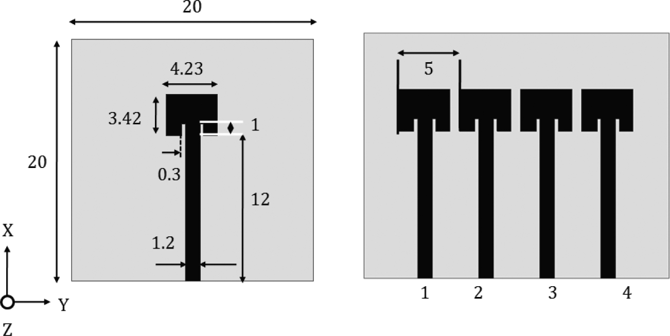
Figure 8.1
Schematic of the inset fed patch antenna and its 1 × 4 array.
The other alternative would be to use a waveguide-based feeding structure such as a substrate integrated waveguide (SIW) or a ridge-gap waveguide. However, the waveguide-based antennas need an additional transition to be incorporated into the feed-line to act as an impedance transformer from the waveguide TEM mode to the antenna. In this example, since the design is PCB based, no additional transition is required.
Figure 8.1 also illustrates the 1 × 4 phased array of patch antennas. The number of elements would primarily decide the gain and beamwidth in the H-plane. As the number of elements increase, so also does the gain. For example, the gain of 4 elements would be 3 dB higher than the gain of 2 elements, which means that as the number of elements is doubled, the gain is also expected to double in a linear scale, translating to 3 dB in a logarithmic scale. As a general rule of thumb, if X dBi is the element gain, then a phased array of 2N elements is expected to have a gain of (X + 3N) dBi in the boresight, which serves as a rough estimate to gauge the number of elements for the desired gain. The estimated gain of (X + 3N) dBi would be feasible only if the elements are impedance matched post-integration, and mutual coupling is minimal, which is never the case in practical designs.
In this example, the antenna elements are separated by 5 mm, which is close to half a wavelength at 28 GHz. The separation is also an important parameter to be considered when designing phased arrays; if the separation is closer than half a wavelength then the beamforming would be inadequate because of the higher mutual coupling. If the elements are placed electrically further away from each other, grating lobes would appear when the ports are excited. Therefore the designer must choose the amount of separation to satisfy both the gain and mutual coupling requirements. The separation is usually fixed at a half wavelength at the centre frequency of operation. The amplitude and phase inputs to the individual ports decide the beamforming.
The broadside beam scanning of the 1 × 4 phased array is shown in Figure 8.2. The individual ports are pumped with equal power without any amplitude distribution. The ports are also fed with a progressive phase shift according to scan angle Equations (8.1) and (8.2), where ‘n’ is the nth port of the phased array, ‘d’ is the separation between the elements, and θsa is the angle at which the resultant beam would be oriented; λ is the free space wavelength computed at the centre frequency of operation. For example, if the beam is scanned at 30°, then θsa = 30°, d = λ/2 hence, φn = nπsin(30°) = (nπ)/2
Figure 8.2
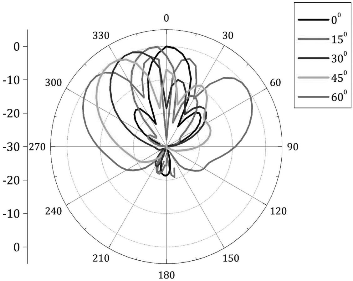
Broadside beam scanning of the 1 × 4 array.
Table 8.1 displays the individual amplitude and phase of the corresponding ports to illustrate the beam scanning principle. The beam scanning for various beam scan angles is illustrated in Figure 8.2; it is apparent that the beamwidth increases as the beam is scanned away from the boresight leading to deterioration in gain, termed as scanning loss. It is also clear that the beam is almost unusable when it is scanned at 60° or higher because of poor beamforming.
Table 8.1
Amplitude and Phase Feeding for 30° Beam Scan
| Port No. | Amplitude | Phase |
|---|---|---|
| 1 | 1 | 0° |
| 2 | 1 | 90° |
| 3 | 1 | 180° |
| 4 | 1 | 270° |
8.3Need for Corner Bent Phased Array
Most of the reported designs based on millimeter wave phased array are planar in nature, which would occupy a large physical footprint in addition to the wastage of radiated power towards the user. Statistically speaking, users would hold the smartphone at an angle of 30° with respect to the horizontal axis. In this situation, if the broadside radiating array is integrated with the panel, the radiation would be targeted towards the user and this would naturally cause a signal blockage as the human body offers a heavy attenuation (30–40 dB) to the millimeter wave signal. The situation is illustrated clearly in Figure 8.3.
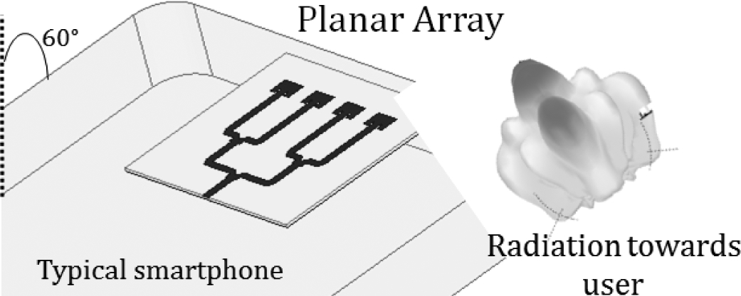
Figure 8.3
Radiation in a real-time scenario for a planar array.
To resolve this issue, an end-fire radiating array could be installed in the panel, such as a printed dipole array, but the physical footprint of the antenna would still be high, reducing the real-estate on the phone for the motherboard and other critical components. Hence the solution to designing a high gain antenna module with beam scanning and minimal footprint is to develop a corner bent broadside array that would radiate away from the user without causing any signal outage. Figure 8.4 gives a clear insight into this design criterion.
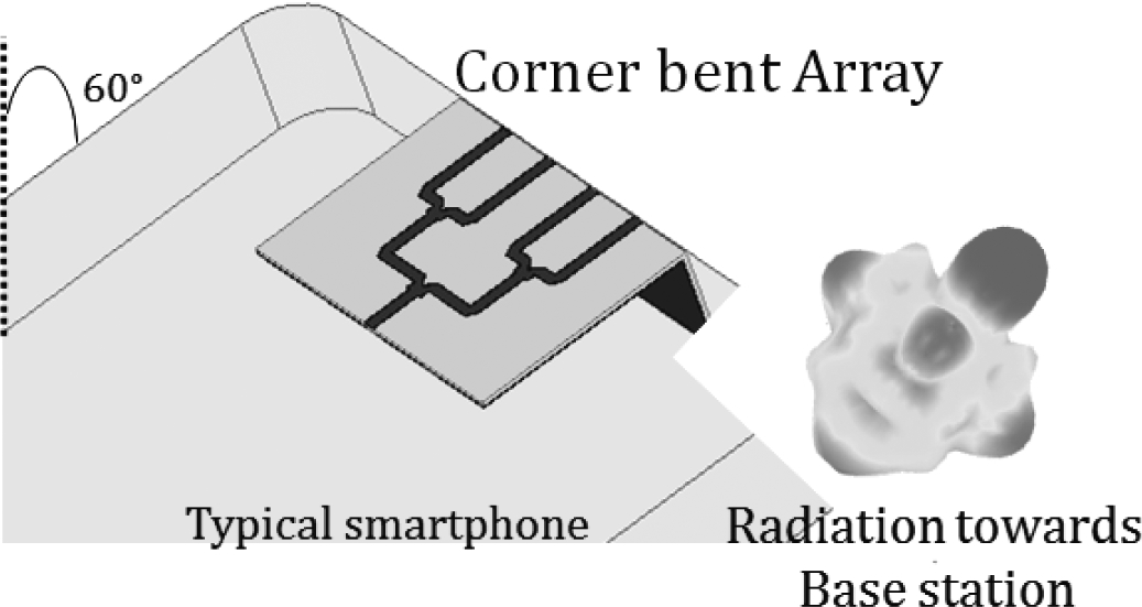
Figure 8.4
Radiation caused by corner bent array on a smartphone.
If the front-to-back ratio of the corner bent array is more than, say, 20 dB, it would mean that significant power is directed towards the base station as against the person using the smartphone. The phase shifters and controllers are not visualized in the design example.
To design the corner bent phased array it is essential to design the antenna on a flexible substrate similar to the antennas designed in section 3.3. The insertion loss is not a critical parameter for stand-alone antennas, or even a diversity module with two or three ports, but it is critical when designing a four-element array. As the number of radiating elements increase, the number of feed-lines and the power dividers would also increase, leading to additional insertion loss and consequently leading to degradation in the boresight gain.
To characterize the relatively low loss polycarbonate substrate, a 50 Ω transmission line is fabricated on a 500 μm substrate, as depicted in the photograph in Figure 8.5, the fabrication of which is identical to the process explained in section 3.3. The length of the transmission line is 50 mm, which translates to 5λ. The insertion loss of the planar transmission line is illustrated in Figure 8.6, indicating a loss of close to 11 dB at 28 GHz. Since the antenna would be designed for corner bending, the transmission line would also be corner bent in the centre, as can be seen from Figure 8.5, and its corresponding insertion loss is also shown in Figure 8.6, indicating a quite close match to its planar counterpart. The loss increases at higher frequencies may be caused by additional radiation from the 90° bending. It is inferred that the bending loss is negligible for the substrate at these frequencies, hence a corner bent array could be designed with this substrate provided the bandwidth is limited to 27–29 GHz for minimal insertion loss resulting from feeding.
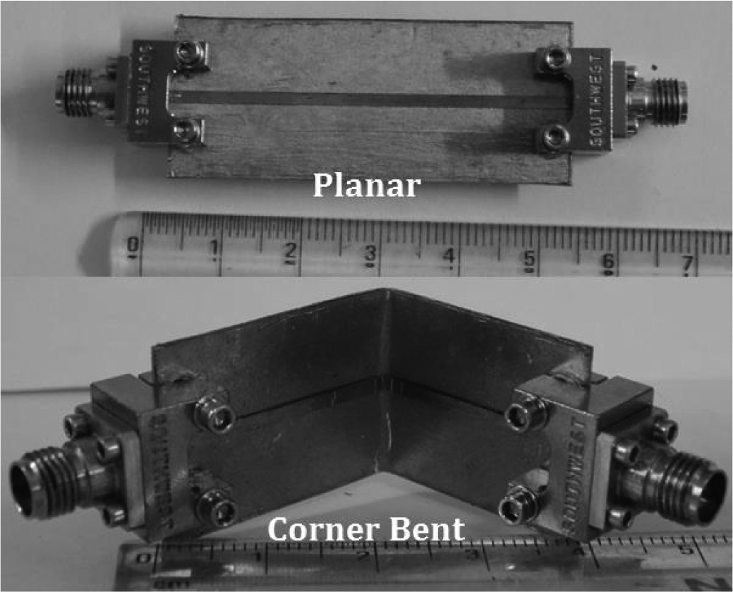
Figure 8.5
Photographs of the transmission lines on polycarbonate substrate.
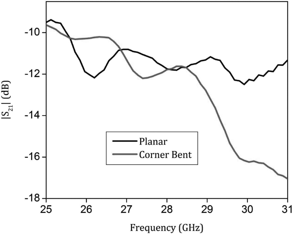
Figure 8.6
Measured insertion loss of planar versus corner bent transmission lines.
8.4Corner Bent Phased Array on Polycarbonate
To design a phased array it is important to first characterize the elements’ characteristics. The antenna element must have a minimal footprint with maximum forward gain achievable. The beam of the single element should be hemispherical, so that when used in the context of a phased array, a low side-lobe main beam could be formed. In this design, the corner bent patch antenna designed on the polycarbonate substrate introduced in section 3.3 is investigated for its suitability as an array element. The schematic and the radiation patterns are depicted in Figure 8.7 and Figure 8.8, respectively.
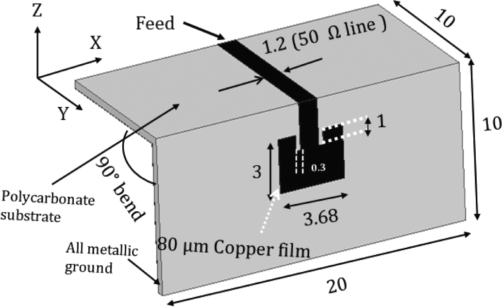
Figure 8.7
Schematic for corner bent inset fed patch antenna.
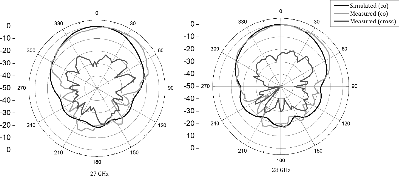
Figure 8.8
Forward H-plane patterns of the corner bent antenna.
It is clear that the forward patterns of the antenna are almost hemispherical, with a high front-to-back ratio of close to 20 dB across the band. It must also be noted that the pattern integrity for the 10% impedance bandwidth is also high, which would translate to a decent beamforming when integrated in an array.
The forward gain is 7 dBi, as illustrated in Figure 8.9, for reasons explained in section 3.3. The gain could have been increased with a lower loss substrate, but the insertion loss post bending would in that case be higher. An electrically thinner substrate would also have given higher gain, but bending would create mechanical stress to the element. Also, mechanical sturdiness is an important design constraint when designing arrays, as phased arrays tend to occupy a larger footprint, and hence require greater mechanical strength.
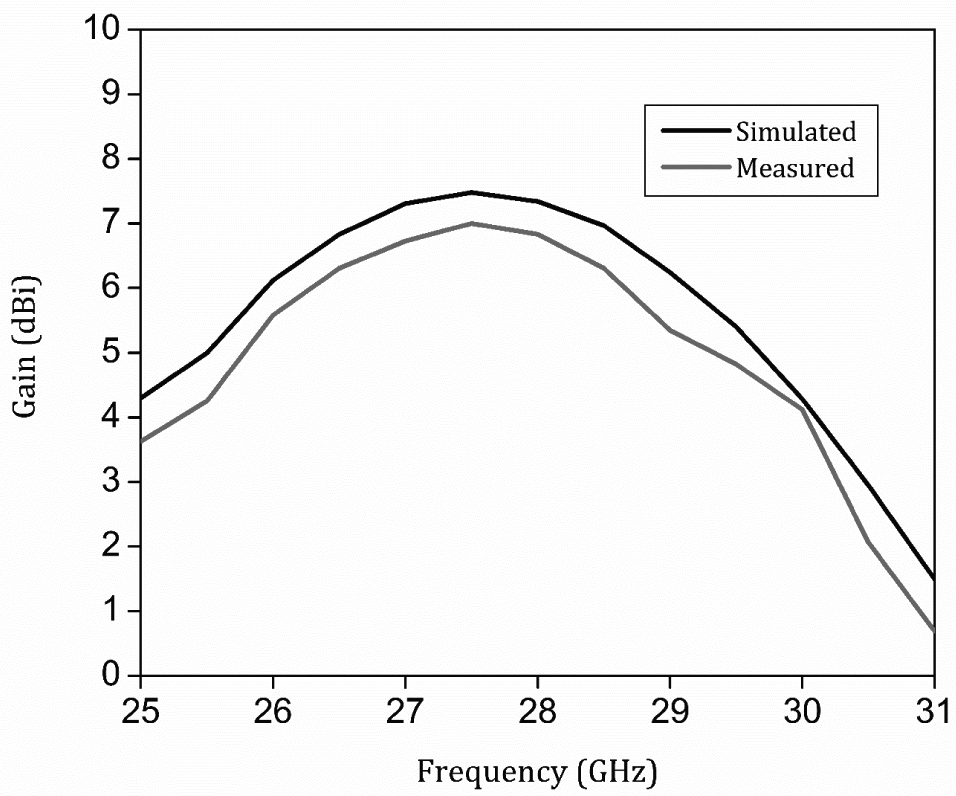
Figure 8.9
Forward gain of the stand-alone antenna element.
The 1 × 4 antenna array is illustrated in Figure 8.10, where the corner bent schematic is also depicted. The fabricated prototype of the flexible array is shown with the end-launch connector in Figure 8.11. Ideally, four different ports have to be designed with individual feeding. This strategy would require four electrically large end-launch connectors along with four expensive transceiver modules.
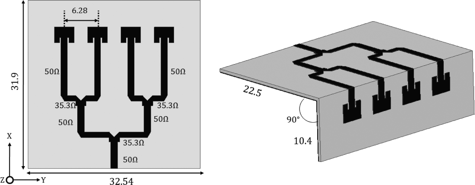
Figure 8.10
Schematic of 1 × 4 antenna array with 0° beam scanning (planar and corner bent).
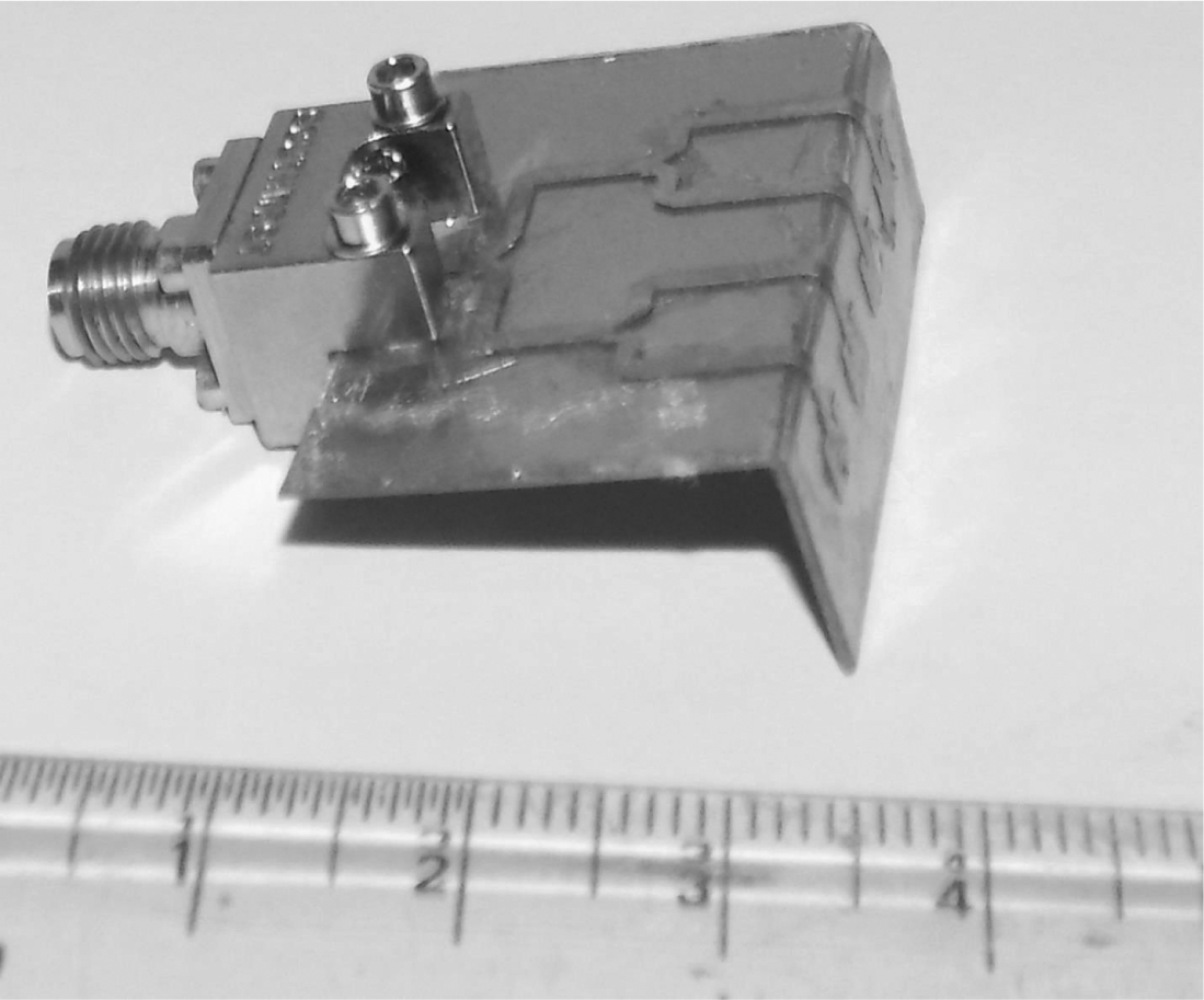
Figure 8.11
Photograph of the corner bent array.
It is a common practice in the antenna community to demonstrate the characteristics of the antenna array with the power divider as seen in the schematics. The feed of the individual antennas are 50 Ω, but the incoming feed line also is designed as a 50 Ω line, thus a two-stage power divider is designed for convenience.
Consider the impedances of antennas 1 and 2, which offer 50 Ω each, and since both of these are in shunt as seen from the feed line, the effective net impedance offered by the combination is 25 Ω, which has to be matched to the 50 Ω line of the left wing of the first power divider. A quarter-wave transformer of impedance 35.35 Ω and 90° length is inserted between the first port of the first power divider and the feed lines of the antenna elements. The same strategy is followed for antenna elements 3 and 4, to achieve impedance matching. The separation between the elements is optimized for 6.28 mm for the reasons mentioned in section 8.2.
The mutual coupling in the power-divider-based array would naturally be higher than the individual ports’ feeding network. It must be noted that the isolation between the fingers of the power divider is not remarkable, as no Wilkinson network is used. If a 100 Ω resistor was used between the antenna elements, isolation between the elements would improve, leading to higher gain in boresight. But resistors would be adding a series inductance post soldering, leading to detuning of the antenna post integration, especially at frequencies beyond 20 GHz, hence resistor design was avoided.
The simulated and measured input reflection coefficients are illustrated in Figure 8.12. The impedance bandwidth is decided primarily by the feed network feeding the elements and the impedance bandwidth of the individual element itself. It is challenging to design a wider bandwidth in the broadside orientation compared to an end-fire antenna.
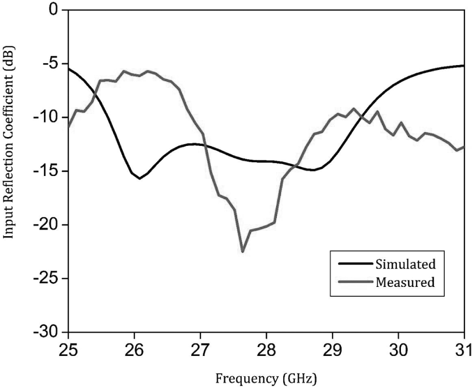
Figure 8.12
Input |S11| of the corner bent array.
The radiation patterns of the boresight scanned phased array at 28 and 29 GHz are shown in Figure 8.13(a) and Figure 8.13(b). The front-to-back ratio is also close to 20 dB as a result of the electrically large ground plane. The side-lobes are caused by scattering of the feed network and the corner bending. It must also be noted that the array was fed with equal amplitude and phase, hence leading to relatively higher side-lobe level. The forward gain of the array is illustrated in Figure 8.14; the boresight gain is 10 dBi at 28 GHz as against 7 dBi of the single element. According to the gain estimation formula mentioned in section 8.2, the gain of the array with power divider should have been 13 dBi, the discrepancy between the estimate and actual design being caused by low isolation between the elements and the high insertion loss of the feeding network.
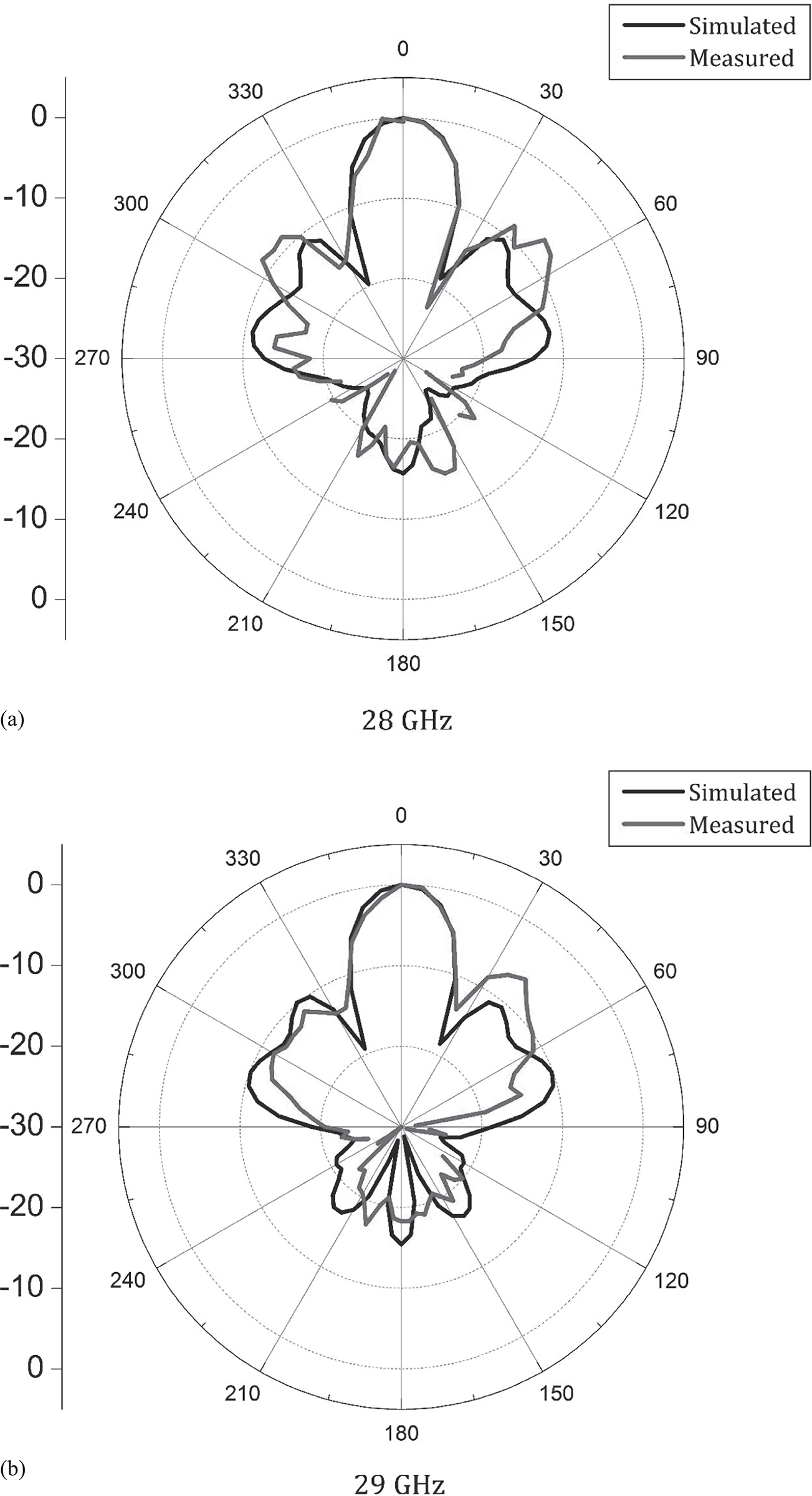
Figure 8.13
(a) H-plane pattern at 28 GHz and (b) H-plane pattern at 29 GHz.
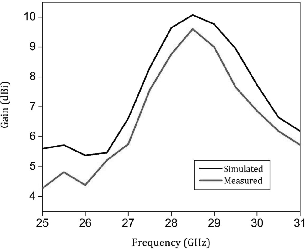
Figure 8.14
Forward gain of the corner bent array.
To demonstrate the beam scanning principle, a 30° beam scanned array is designed as shown in Figure 8.15, along with its corresponding pattern in Figure 8.16. The progressive phase shift indicated in Table 8.1 is implemented as delay lines in the feeding lines of the respective antennas.
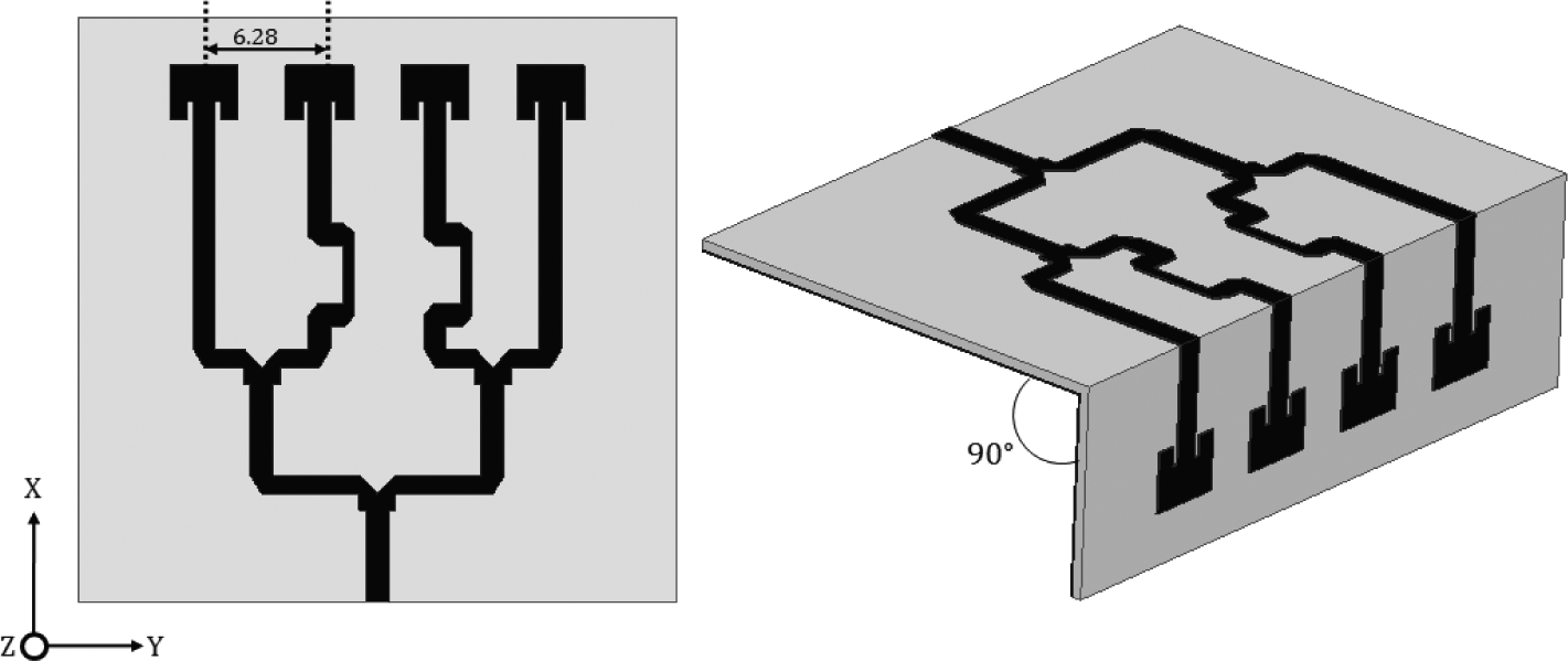
Figure 8.15
Schematic of 1 × 4 antenna array with 30° beam scanning (planar and corner bent).
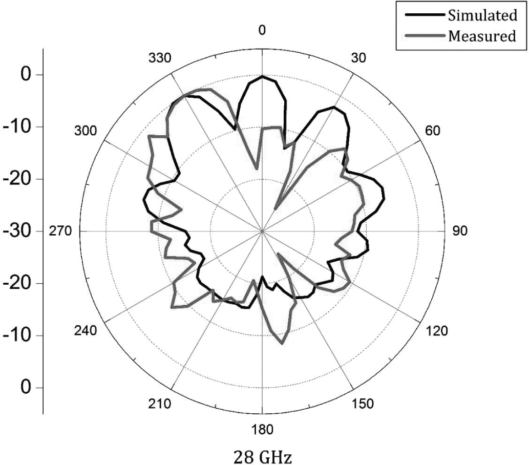
Figure 8.16
Forward pattern for the 30° beam scanned corner bent array.
8.5Design Guidelines for a Phased Array at Ka Band
-
Antenna element design must operate in the specified band with a hemispherical beam and maximum gain for the available aperture. The antenna must be matched to the standard 50 Ω as this would be easier for scaling up the design in an actual phased array.
-
The specified gain decides the number of elements required to achieve that gain. Simple calculations must give an estimate regarding the number of elements; additional elements might be required to compensate for the insertion loss.
-
The feed network must to be designed with power dividers and additional matching circuits as necessary.
-
The beam forming must be characterized for beam scanning and scanning loss across frequency of interest.
8.6Conclusion
In this chapter, the principle of phased arrays was introduced, followed by design criteria for phased array design specifically at mmWave 5G frequencies. The principle for beam scanning with respect to a generic 1 × 4 inset fed patch antenna array was also discussed. The need for a corner bent phased array topology was also discussed with justification. A corner bent phased array on a flexible substrate was demonstrated with a power divider network. The guidelines for designing a phased array for Ka band was also discussed.
References
- 1.R. J. Mailloux, Phased Array Antenna Handbook, Norwood, MA, USA, Artech House, 1994.
- 2.R. C. Hansen, Phased Array Antennas, New York, Wiley, 1998.
- 3.W. Hong, K. Baek, Y. Lee, Y. Kim, and S. Ko, “Study and prototyping of practically large-scale mmWave antenna systems for 5G cellular devices,” IEEE Communications Magazine, 52(9), 63–69, September 2014.
- 4.S. F. Jilani and A. Alomainy, “Planar millimeter-wave antenna on low-cost flexible PET substrate for 5G applications,” 2016 10th European Conference on Antennas and Propagation (EuCAP), Davos, 1–3, 2016.
- 5.S. F. Jilani, M. O. Munoz, Q. H. Abbasi and A. Alomainy, “Millimeter-wave liquid crystal polymer based conformal antenna array for 5G applications,” IEEE Antennas and Wireless Propagation Letters, 18(1), 84–88, January 2019.
- 6.S. X. Ta, H. Choo, and I. Park, “Broadband printed-dipole antenna and its arrays for 5G applications,” IEEE Antennas and Wireless Propagation Letters, 16, 2183–2186, 2017.
- 7.S. Zhu, H. Liu, Z. Chen, and P. Wen, “A compact gain-enhanced vivaldi antenna array with suppressed mutual coupling for 5G mmWave application,” IEEE Antennas and Wireless Propagation Letters, 17(5), 776–779, May 2018.
- 8.B. Yang, Z. Yu, Y. Dong, J. Zhou, and W. Hong, “Compact tapered slot antenna array for 5G millimeter-wave massive MIMO systems,” IEEE Transactions on Antennas and Propagation, 65(12), 6721–6727, December 2017.
- 9.M. Sun, Z. N. Chen, and X. Qing, “Gain enhancement of 60-GHz antipodal tapered slot antenna using zero-index metamaterial,” IEEE Transactions on Antennas and Propagation, 61(4), 1741–1746, April 2013.
- 10.R. A. Alhalabi and G. M. Rebeiz, “High-efficiency angled-dipole antennas for millimeter-wave phased array applications,” IEEE Transactions on Antennas and Propagation, 56(10), 3136–3142, October 2008.