
4
Mobile RF Transmitter and Receiver Design Solutions
4.1 Introduction to RF Transceiver
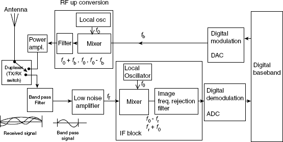
In Section 1.3.3.2 of Chapter 1, we discussed the basic building blocks of a mobile phone. For a digital mobile phone, the modem part can be broadly divided into two main blocks: (a) the RF module and (b) the baseband module. The RF module is the analog front-end module. On the receiver side it is responsible for signal reception from the air and down conversion onto the baseband signal, and on the transmitter side it is responsible for up conversion of the baseband signal to the RF signal, then transmission in the air. The baseband module deals with digital processing of the baseband signal and protocols. An ADC and DAC are placed in between the analog RF and digital baseband units. In this chapter, we will discuss the different design solutions for analog RF front-end modules. The basic building blocks of a typical radio RF front-end section of any mobile device (using digital baseband) is shown in the Figure 4.1.
- Antenna – This acts as a transducer. It converts the incoming EM wave into an electrical signal on the receiver side and the outgoing electrical signal into an EM wave on the transmitter side. The basic principle of antenna action has already been discussed in Chapter 1, and different types of mobile phone antennas are discussed in detail in Chapter 10.
- Tx–Rx Path Separation Block (Duplexer or Tx–Rx Switch or Diplexer) – Generally the same antenna is used for transmission as well reception purposes. So we have to have a mechanism to multiplex the same antenna between the transmit and receive path. There are several techniques available:
- Tx–Rx Switch – Here the same antenna is time switched between the Rx and Tx paths (Figure 4.2). Systems where the Tx and Rx path signals are not present simultaneously (for example, a half duplex system GSM), then a Tx–Rx switch can be used. Diodes can be used as switching elements and switching is controlled by the processor to connect the Tx or Rx path with the antenna. Single frequency can also be used for Tx and Rx, which is suitable for a time division based system.
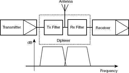
- Diplexer – The Tx and Rx frequency bands are different and they are first separated by filters and then connected to the Rx or Tx path (Figure 4.3). It only works for systems with separated Rx and Tx frequency bands (FDD).
Figure 4.1 Various blocks of an RF transceiver (analog front end)
Figure 4.2 Antenna multiplexing by using a Tx–Rx switch
- Duplexer – The Tx circuit, Rx circuit, and antenna are connected to the three port duplexer (Figure 4.4). Tx and Rx are separated by a path difference of λ/2 = phase difference of “π”, for example, they are opposite in phase (−ve) and will cancel each other out. Thus the Tx port is isolated from the Rx port, but the signal from Tx and Rx will arrive at the antenna at same phase (π/2) as the path difference between Tx or Rx with an antenna port is λ/4.
Figure 4.4 Duplexer
A comparison of these three techniques for antenna multiplexing between Tx and Rx path is given in the Table 4.1.
Electrically a duplexer is a device that uses sharply tuned resonate circuits to isolate the transmitter circuit from the receiver circuit. This allows both of them to use the same antenna at the same time without the transmitter RF frying the receiver circuit. The separation or isolation between the transmit and receive signal paths is mandatory in order to avoid any destruction of the receiver when the Tx signal is injected, or at least to avoid any degradation of the receiver sensitivity due to the frequency proximity of the high power signal from the transmitter block.
Table 4.1 Comparison between different antenna multiplexing techniques
In the cellular band, the duplexer's jobs are: (1) to isolate the transmitted signal from the received signal in the receive band to avoid any degradation of the receiver sensitivity; (2) attenuating the power amplifier (PA) output signal to avoid driving the low-noise amplifier (LNA) into compression; (3) attenuating the receiver's spurious responses (first image and others); (4) attenuating first local oscillator (LO) feed-through using the first mixer LO-RF ports; and (5) attenuating transmitter output harmonics and other undesired spurious products.
- Band-Pass Filter – This is used to extract the desired band of signal from the entire band of the received signal. Whatever EM waves impinge on the antenna, based on their length (~wavelength) the antenna will convert those waves into RF electrical signals. In the reception path there will be many such RF signals with different frequencies, which will be mixed up and appear in the receiver circuit. Out of these, we need to take only the desired frequency band by using an appropriate band-pass filter.
- Low-Noise Amplifier – The amplitude of the received signal will be much less. So we need to boost this received feeble signal without adding any extra noise signal into it, for example, this stage of amplification should have a very low level of noise. This is why we use a low-noise amplifier (LNA).
- Mixer – Mixers are key components in receivers as well as in transmitters. Mixers translate the signals from one frequency band into another, by mixing frequencies. The output of the mixer consists of multiple images of the input signals to the mixer, where each image is shifted up or down by multiplication of the local oscillator (LO) frequency. The mixer's output signals are usually the signals translated up and down by one LO frequency. Generally mixers (sometimes known as frequency converters), modulators, and balanced modulator circuits work on the same basic principle.
This module contains local oscillators to generate RF signal locally and mixers to mix the incoming and locally generated LO signal in order to down convert the incoming RF signal. Suppose the received RF signal is Ar sinωrt and the local oscillator signal is Ao sinωot. If these are mixed (that is, multiplied) the resultant signal will be Ar sinωrt. Ao sinωot = (ArAo/2) cos2 π (fo − fr) t + cos2 π (fo + fr) t. That means it generates two frequencies (fo − fr) and (fo + fr). This signal is passed through a channel select filter, which will filter out the frequency (fo + fr), so that only (fo − fr), known as the intermediate frequency (IF) will be passed forward. In some receivers, two or more such IF stages are used. Thus the RF signal is down converted in several steps and finally it arrives at the last stage, where the (fo − fr) becomes equal to the baseband signal frequency fbaseband. This is then sampled at a minimum rate of 2 * fbaseband = Nyquist rate, to recover the baseband data signal and then digitally demodulated. Similarly, the mixer is used for frequency up conversion in the Tx path.
In an ideal situation, the mixer output would be an exact replica of the input signal. However, the reality is that the mixer output is distorted due to non-linearity in the mixer. In addition, the mixer components and a non-ideal LO signal introduce more noise in the output. Bad design might also cause leakage effects, complicating the design of the complete system. The mixer design is discussed in more detail in Section 4.2.
- Digital Demodulation – For the receiving system, which uses digital technology, the received analog signal is digitally demodulated. Various techniques are used for digital modulation–demodulation, such as ASK, FSK, PSK, QPSK, MSK, GMSK, and QAM. Modulation/demodulation has already been discussed further in Chapter 3.
- A/D Converter – The received signal is sampled and converted into a digital signal. There are different types of ADC used for this purpose. Among these, sigma delta is very popular, which is discussed in Chapter 10.
- Digital Modulation – The transmitted digital data from the baseband is digitally modulated using different digital modulation techniques.
- D/A Converter – This converts the baseband digital signal into a baseband analog signal.
- Power Amplifier – The feeble RF signal is amplified to high power by a power amplifier, sent to a duplexer unit, and then to an antenna.


4.2 Mixer Implementations
The mixer is implemented using various properties, and below some commonly used mixer implementations are discussed.
Ideal Mixer – The ideal mixer will perform the mathematical multiplication of the two input signals, creating components positioned at frequencies equal to the sum and difference of the input signals with no additional components. This is why the mixing (multiplying) device must be perfectly linear and there must be no leakage of the input signals to the output port.
Single Balanced Mixer and Double Balanced Mixer – The term balanced mixer is used to imply that neither of the input terms will appear at the mixer output. However, in practice, suppression of these input components is never perfect in an analog mixer circuit. A balanced mixer can be implemented using a transformer coupled diode arrangement, or by using an active transistor based design. Both types of mixer produce signals at odd harmonics of the carrier frequency, particularly the diode ring mixer. In most instances, these can be easily filtered out.
The single balanced mixer (SBM) performs multiplicative mixing because its RF and LO signals are applied to different ports. This is more commonly seen in two diode mixer configurations, a balanced transformer drives the diodes out of phase for the LO and in phase for signals present at the RF port. Adding two more diodes and another transformer to the singly balanced mixer results in a double balanced mixer (DBM), as shown in Figure 4.5. Its frequency response is largely determined by the frequency response of its transformers. As second-order harmonics are the most difficult to suppress, so double balanced mixers are the favored solution.

Figure 4.5 Double-balanced mixer
4.2.1 Design Parameters
The mixer performance is dependent on parameters such as conversion loss, isolation, dynamic range, dc offset, dc polarity, two-tone third-order inter-modulation distortion, and intercept point. Although a mixer works by means of amplitude non-linear behavior, we generally want it to act as a linear frequency shifter. The degree to which the frequency-shifted signal is attenuated or amplified is an important parameter in mixer design. A mixer also contributes noise to the output frequency shifted signals. The degree to which a mixer's noise degrades the SNR of the signals is evaluated in terms of noise factor and noise figure. The load presented by a mixer's ports to the outside world can be of critical importance to a designer for VSWR matching. Isolation between ports plays a major role in reducing dc offset in a mixer. The dynamic range of any RF/wireless system can be defined as the difference between the 1 dB compression point and the minimum discernible signal.
4.2.1.1 Inter-Modulation Distortion and Intercept Points
If there is a large interfering signal presents within the bandwidth of the RF input filter, then mixer distortion heavily limits the sensitivity of a receiver. There are two aspects of distortion that are of concern: (1) compression, and (2) inter-modulation distortion. The 1 dB compression point (CP1) is the point where the output power of the fundamental crosses the line that represents the output power extrapolated from small-signal conditions minus 1 dB. The third-order intercept point (IP3) is the point where the third-order term, as extrapolated from small-signal conditions, crosses the extrapolated power of the fundamental. Both CP1 and IP3 illustrated in Figure 4.6.

Figure 4.6 Intercept points
Distortion of the output signal occurs, because several of the odd-order inter-modulation tones fall within the bandwidth of the circuit. Inter-modulation distortion is typically measured in the form of an intercept point. As shown in Figure 4.6, the third-order intercept point (IP3) is determined by plotting the power of the fundamental and the third-order inter-modulation product versus the input power.
4.2.1.2 Basic Difference Between Mixer and an Amplitude Modulator
The mixer and AM modulator work in the same fashion and generate three output signal frequencies. The only difference is that in a mixer the two different signals are multiplied (Ar sinωrt Ao sinωot), whereas in an AM modulator the amplitude of the RF carrier signal is varied according to the input signal: v(t) = A(1 + m sinωmt) sinωct.
4.3 Receiver Front-End Architecture
In the previous section, we saw the various blocks of a radio receiver. The receiver architecture mainly varies based on the RF front end.
4.3.1 Different Types of RF Down Conversion Techniques
Typically, radio communication systems operate with carrier frequencies at many hundreds of MHz to several GHz. If we want to sample the received signal at the antenna itself (this will help to bypass RF hardware blocks and will help to process everything in the digital domain, which is most desirable for software defined radio), then the minimum sampling frequency requirement will be 2*fs (~2*1 GHz, for example, 2 giga samples will be generated per second and then each sampled level will be converted into several bit streams by the ADC), and the sampled data will be too huge to handle by any of the present day's DSP (digital signal processor). Also, directly converting the antenna signals into digital form in an integrated ADC would require prohibitively large sensitivity, selectivity, linearity, and very high conversion speed. As of today, such analog-to-digital converters that could offer this services do not exist. As a result, the received RF signals need to be converted into lower frequencies (baseband frequency), for the signal processing steps, such as channel selections, amplification, and detection. This conversion is accomplished by a mixing process, producing a down-converted (in the receiver block) and an up-converted (used in the transmitter block) component.
Now, based on the mixing of the local oscillator (LO) frequency with the desired incoming RF frequency, several down-conversion techniques exist. We can mainly classify these into two broad categories: heterodyne and homodyne receivers. (1) In a heterodyne receiver the LO frequency and desired RF frequency is set to be different –examples of such architecture are super heterodyne, low IF, and wide IF receivers. (2) Whereas in the case of a homodyne receiver (same mixing) the LO frequency and the desired RF frequency are set to be the same, so the IF (intermediate frequency) is zero. Prior to the selection of optimum receiver architecture, different types of RF down-conversion receiver architectures will be reviewed and compared.
4.3.1.1 Heterodyne Receiver
Conventional radio receivers utilize the so called heterodyne architecture (hetero = different, dyne = mix). This architecture, translates the desired RF frequency into one or more intermediate frequencies, before demodulation.
What is Heterodyning? – “Heterodyne” means mixing two different frequencies together (one incoming signal frequency from the antenna and other locally generated from the local oscillator), to produce a beat frequency, namely the difference between the two and the sum of the two. Example: Ar sin ωrt Ao sin ωot = (ArAo/2) cos 2 π (fo − fr) t + cos 2 π (fo + fr) t.
What is Superheterodyning? – When we use only the lower sideband (the difference between the two frequencies), we are superheterodyning. Strictly speaking, the term superheterodyne refers to creating a beat frequency that is lower than the original signal. Edwin Armstrong came up with the idea of converting all incoming frequencies into a common frequency. The superheterodyne receiver, invented in 1917, has enjoyed a long run of popularity.
We have discussed that superheterodyning is simply reducing the incoming signal frequency by mixing. In a radio application (Figure 4.7), we are reducing the incoming AM or FM signal frequency (which is transmitted on the carrier frequency) to some intermediate frequency, called the IF (intermediate frequency) = fo − fr.

Figure 4.7 Basic block diagram of a super-heterodyne receiver (analog receiver)
This is essentially the conventional receiver with the addition of a mixer and a local oscillator. The local oscillator is linked to the tuner, because they must both vary with the carrier frequency. Let us look at a specific example. An FM radio is tuned to a station operating at 89.9 MHz. This signal is mixed with an LO signal at a frequency of 100.6 MHz. The difference frequency at the output of the mixer is 10.7 MHz. This is the IF signal. If the FM radio is tuned to a different station at 107.9 MHz, the LO frequency is also re-tuned to 118.6 MHz. The mixer once again produces an IF signal of 10.7 MHz. In fact, as the FM radio is tuned across the band from 87.9 to 107.9 MHz, the local oscillator (LO) is tuned from 98.6 10 118.6 MHz. No matter what frequency the radio is tuned to (in its operating range), the mixer's output will be 10.7 MHz.
The superheterodyne overcomes the variable sensitivity and selectivity problems of the RF receiver module by doing most of the amplification at the intermediate frequency, where the gain and selectivity can be controlled carefully (Figure 4.8). However, the superheterodyne introduces some new challenges. Firstly, the LO signal must always differ from the input signal by exactly the IF frequency, regardless of whatever input frequency is selected. This is known as “tracking”. Secondly, there are two different frequencies that can mix with the LO signal to produce the IF signal. One of these frequencies is our input signal frequency; the other is known as the “image frequency.” The image, input, IF, and LO frequencies are related as follows.

Figure 4.8 Super-heterodyne receiver architecture (digital receiver: I–Q modulated)
The image is another incoming frequency that is mistakenly treated as the desired input signal.
IF = LO−input : IF = image−LO; for example; image = IF+LO = IF+IF+input: Thus; image = input+2*IF
Let us take an example that references our earlier discussion about the FM radio. When the receiver is tuned to 89.9 MHz, the 89.9 MHz signal can mix with the LO signal of 100.6 MHz to create a 10.7 MHz IF signal. However, a signal (or noise) at 111.3 MHz can also mix with the LO signal to create a 10.7 MHz IF. Therefore, any incoming noise or interference signals at this frequency have to be rejected. One filter is used to stop (f0 + fi) and pass (f0 − fi) to the demodulator unit. fif = f0 − fi, which is allowed to pass, but there may be another frequency that is (f0 + fif) when this is input to the mixer, then the resultant will be (f0 + fif) − f0 = fif. Thus this will also pass via the filter. However here, IF is not because of the desired input signal (fi) rather it is another input signal (f0 + fif). This is known as image frequency as discussed earlier (f0 + fif) = fimage. This also needs to be rejected as it causes the following issues.
Image Frequency Problem
The desired RF input signal frequency = fif = f0 − fi (which is allowed to pass via the filter). However, there is another RF input signal frequency f0 + fif = fimage, and when this is fed to the mixer, the resultant frequency = f0 − fimage = f0 − f0 + fif = fif. As this resultant frequency is same as the IF frequency, so this will also pass via the filter (Figure 4.9). This is derived from unwanted RF signal, and is known as the image frequency, which needs to be stopped, otherwise this will corrupt the original signal and appear in the detector.

Figure 4.9 Image frequency
To reject the mirror/image frequency signal, an additional filter is often applied as front of the mixer, which is known as an image rejection filter (IR). This is bulkier and makes the on-chip integration difficult.
On-Chip Superheterodyne Receiver Architecture
The on-chip architecture of the above discussed superheterodyne receiver is shown in Figure 4.10. A passive band-pass filter limits the input spectrum provided by the antenna. Noise is introduced into the mixer, so the signal is first amplified by a low-noise amplifier (LNA) before mixing. Mixers translate the RF signal into IF frequencies. The LO signal, which is tuned at a particular spacing above or below the RF signal, is injected into the mixer circuits. Hence, first these bands have to be removed by an image reject filter. For this, the signal goes off-chip into an image rejection (IR) filter using passives with high-quality factors. Then, on mixing with a tuneable LO signal, the selected input channel frequency is down converted to an IF. This LO1 output needs to be variable in small frequency steps for narrow band selection. To alleviate the aforementioned sensitivity–selectivity trade-off in image rejection, an off-chip, high-Q band-pass filter performs partial channel filtering at a relatively high intermediate frequency. A second down-conversion mixing step translates the signal down to baseband frequency, which can be treated in the digital domain. This reduces the requirement for the final, integrated analog channel selection filter, as now it can be done digitally.

Figure 4.10 Heterodyne RF converter (with on-chip and off-chip components)
Digital modulation schemes, which use both in-phase (I) and quadrature (Q) elements of a signal, and thus both components can be generated in the second mixing stage, as shown in Figure 4.10. As the channel of interest has already been selected by the first mixer, the frequency of the second LO is fixed.
Off-chip passive components provide filters with a high Q-factor and result in good performance for both sensitivity and selectivity, which makes the heterodyne architecture a common choice. Furthermore, noise introduced by the local oscillator is less problematic, as it is filtered by the subsequent channel selection. Image rejection and adjacent channel selectivity is better in this type of architecture. The filters can be manufactured using different technologies such as SAW (surface acoustic wave external filter), bipolar, and CMOS. However, off-chip filtering comes at the expense of extra signal buffering (driving typically 50 ohm loads), increased complexity, higher power consumption, and larger size. Narrow-bandwidth passive IF filtering is typically accomplished using crystal, ceramic, or SAW filters (these are passive filters). These filters offer better protection than the receivers of zero-IF gyrator filters (active filter) against signals close to the desired signal because passive filters are not degraded by the compression of a signal resulting from large signals. The active gyrator circuit does not provide such protection.
However, undesired signals that cause a response at the IF frequency in addition to the desired signal are known as spurious responses. In the case of the heterodyne receiver, spurious responses must be filtered out before reaching the mixer stages. One spurious response is known as an image frequency. An RF filter (known as a pre-selector filter) is required for protection against the image unless an image-reject mixer is used. Additional crystal-stabilized oscillators are required for the heterodyne receiver.
Generally, superheterodyne (superhet) receivers cost more than zero-IF receivers due to the additional oscillators and passive filters. These items also require extra receiver housing space, for example, increased size. However, the superior selectivity of a superheterodyne receiver may justify the greater cost and size in many applications.
The benefits of the superhet architecture are enormous: Most of the filtering and gain takes place at one fixed frequency, rather than requiring tunable high-Q band-pass filters or stabilized wideband gain stages. In some systems, multiple IFs are used to distribute the gain and selectivity for better linearity.
Advantages and Disadvantages of Superheterodyne Receiver
Advantages – High selectivity and sensitivity as a result of the use of high-Q filters and the double RF down conversion scheme. (2) Good image rejection capability.
Disadvantages – Image frequency problem; to reject the mirror frequency signal (image frequency) an additional filter (IR) is often applied in front of the mixer. (2) Poor integration; port integration becomes difficult as it uses high-Q devices, a double conversion scheme, IR, and channel filter (passive). Hence, it cannot be integrated in small packages such as inside a chip or set of chips. (3) Larger in size and weight. (4) It consumes more direct current (dc) power. (5) Only a fixed data bandwidth. (6) Higher cost for higher number of components, improved protection and larger physical size, requires extra printed circuit board (PCB) real estate.
Applications – The superhet receiver is typically used in radio receivers and satellite receivers.
4.3.2 Homodyne Receiver
4.3.2.1 Zero-IF Receiver (DCR)
The homodyne (homo = same, dyne = mix) architecture uses a single frequency translation step to convert the incoming RF channel directly into baseband, without any operations at intermediate frequencies. It is therefore also called as zero-IF or direct conversion receiver (DCR) architecture. Here, the IF frequency is chosen as 0 Hz (dc frequency) by selecting the local oscillator frequency to be the same as the desired RF input signal frequency. So after mixing at both I and Q channels, the generated frequency components will be (f0 − fi) = 0, and (f0 + fi) = 2fi as f0 = fi. This is shown in Figure 4.11. The portion of the channel translated into the negative frequency half-axis becomes the image to the other half of the same channel translated into the positive frequency half-axis. After the down conversion the input signal has a bandwidth of B Hz around the center 0. Figure 4.12 shows this architecture in the case of quadrature down conversion (I–Q de-modulation receiver) receiver. As with the heterodyne receiver, in this architecture an off-chip RF filter first performs band limitation, before the received signal is amplified by an integrated LNA. Channel selection is done by tuning the RF frequency of the LO to the center of the desired channel, making the image equal to the desired channel. Thus in this situation the problem of images is not present and the off-chip IR filter can be omitted. A subsequent channel selection low-pass filter (LPF) then removes nearby channels or interferers prior to A/D conversion.
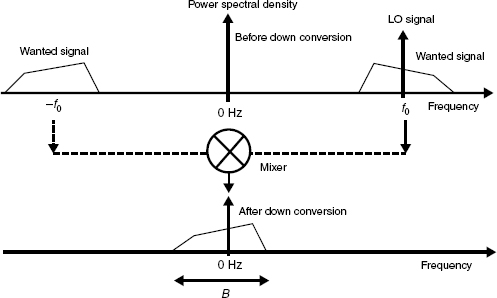
Figure 4.11 Direct conversion technique
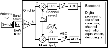
Figure 4.12 On-chip zero-IF direct conversion RF converter
Owing to the direct conversion to DC, homodyne receivers are more susceptible to disturbances arising from I/Q phase mismatches, non-linearities, and flicker noise, than heterodyne designs. To control the performance loss, additional circuitry and design efforts are required. However, there is no need for image rejection or other off-chip filters, which helps to save power and reduces the total receiver size.
Advantages of this Architecture
- No image frequency problem – an advantage of the zero-IF receiver is that no image exists and an image-reject filter (or image-reject mixer) is not required.
- LPF can be integrated – channel filtering is now possible entirely on-chip as after the down conversion the frequency is now at the baseband frequency. The zero-IF receiver can provide narrow baseband filtering with integrated low-pass (LP) filters. Often the filters are active op-amp-based filters known as gyrators. The gyrators provide protection from most undesired signals. The gyrator filters eliminate the need for expensive crystal and ceramic IF filters, which take up more space on a printed circuit board.
- Eliminate passive IF and image-reject filter – the IF SAW filter, IR filter, and subsequent stages are replaced with low-pass filters (LPF's) and baseband amplifiers that are amenable to monolithic integration. The LNA need not drive a 50 ohm load because no image rejection filter is required.
- Increased ADC dynamic range because of limited filtering.
- Good SSB digital modulation.
- Reduced component numbers.
- Reduced power consumption – the filtering and gain can now take place at dc, where gain is easier to achieve with low power, and filtering can be accomplished with on-chip resistors and capacitors instead of the expensive and bulky SAW filters.
- High level of integration – the zero-IF topology offers the only fully integrated receiver currently possible. This fully integrated receiver solution minimizes the required board real estate, the number of required parts, receiver complexity, and cost. Most zero-IF receiver architectures also do not require image-reject filters, thus reducing cost, size, and weight.
- Good multi-standard ability – the placement of the filter at the baseband (usually split between the analog and digital domains) permits multiple filter bandwidths to be included at no penalty to the board area, as the filtering is accomplished on-chip. Thus, direct conversion is the key to multimode receivers for the future.
Problems of this Architecture and Possible Alternative Design Solutions
Several well known issues that have historically plagued direct-conversion receivers are: self-detection due to LO-RF leakage, dc offset, and AM detection.
- Local Oscillator Leakage – One of the most well know problems in direct-conversion receiver architecture is the spurious LO leakage. This arises because the LO in a direct-conversion receiver is tuned exactly to the desired input signal frequency, which is the center of the LNA and antenna pass-band. Owing to imcorrect isolation, a small fraction of this LO signal leaks through the mixer and travels towards the input signal side, passes through the LNA and arrives at the antenna (Figure 4.13). Then it radiates out through the antenna. This becomes an in-band interferer to other nearby receivers tuned to the same band, and for some of them, it may even be stronger than the desired signal. Regulatory bodies, such as the FCC strictly limit the magnitude of this type of spurious LO emission. Each wireless standard and the regulations of the Federal Communications Commission (FCC) impose upper boundariess on the amount of in-band LO radiation, typically between 50 and 80 dBm. The issue is less severe in heterodyne and image-reject mixers because their LO frequency usually falls out of the reception band. Also, it leaks to other side of the entire receiver signal chain, which appears as a dc offset. The problem of LO leakage becomes severe as more sections of the RF transceivers are fabricated on the same chip.
Figure 4.13 LO leakage
Design Option – With differential local oscillators, the net coupling to the antenna can approach acceptably low levels.
- Self-reception – Because the local oscillator is tuned to the RF frequency, self-reception may also be an issue (Figure 4.14).
Figure 4.14 (a) Self-mixing LO and (b) interferers mixing
Design Option – Self-reception can be reduced by running the LO at twice the RF frequency and then dividing by two before injecting into the mixer. Because the zero-IF local oscillator is tuned to RF frequencies, the receiver LO may also interfere with other nearby receivers tuned to the same frequency. However, the RF amplifier reverse isolation prevents most LO leakage to the receiver antenna.
- Dc Offset Problem – The basic operation of a direct-conversion receiver can be described as mixing an input signal frequency of (fC + fm), where fm is the bandwidth of the modulation, with a local oscillator at fLO, yielding an output at fMIXOUT = (fC + fm – fLO) and (fC + fm + fLO). The second term is at a frequency twice that of the carrier frequency and can be filtered out very easily by the channel select filter. However, the first term is much more interesting, as fLO = fC, and substitution yields fMIXOUT = fLO + fm − fLO = fm. This means that the modulation has been converted into a band from dc to the modulation bandwidth, where gain, filtering, and A/D conversion are readily accomplished. The dc-offset problem occurs when some of the on-channel LO (at fC) leaks to the mixer RF port, creating the effect that fLO − fLO = 0 (or dc). This can corrupt desired information that has been mixed down around zero Hz.
So, when the leaked LO signal appears at the input of the mixer, then leaked LO signal and LO signal are mixed, this will result in a zero frequency output or dc output as they are at same frequency. Also, remember, in DCR the desired down converted signal is centered around zero frequency. Thus, self-mixing caused by leakage from the local oscillator to the LNA (or vice versa) will corrupt the baseband signal at dc and saturate subsequent processing blocks. This leads to a narrower dynamic range of the electronics, because the active components become saturated easier than in the case of a zero offset.
Dc offsets is a severe problem in homodyne receivers. If the receiver moves spatially, it receives reflected LO signals at the antenna, which generates time varying offsets. Causes of dc offset are either drift in the baseband components (for example, op amps, filters, A/D converters), or dc from the mixer output caused by the LO mixing with itself or with the mixers acting as square law detectors for strong input signals. Dc offsets from various sources lie directly in the signal band, and in the worst case they can saturate the back-end of the receiver at high gain values.
Design Options – From the above discussion, we infer that DCRs require some means of offset removal or cancellation.
- Ac Coupling: A possible approach to remove the offset is to use ac coupling, that is, high-pass filtering, in the down-converted signal path. However, as the spectrum of random binary (or M-ary) data exhibits a peak at dc, such a signal may be corrupted if it is filtered with a high corner frequency.
One technique is to disregard a small part of the signal band close to dc and employ a high-pass filter with a very sharp cutoff profile at low corner frequencies. This requires large time constants, and hence, large capacitors, that is, area. It is only practical for wideband applications (WCDMA), where the loss of a few tens of hertz bandwidth at dc does not degrade the receiver performance significantly. The system can either be ac coupled or incorporate some form of dc notch filtering after the mixer. However, for narrow band applications (GSM), this would cause large performance losses.
A low corner frequency in the HPF may also lead to temporary loss of data in the presence of the wrong initial conditions. If no data are received for a relatively long time, the output dc voltage of the HPF drops to zero. Now if data are applied, the time constant of the filter causes the first several bits to be greatly offset with respect to the detector threshold, thereby introducing errors.
A possible solution to the above problems is to minimize the signal energy near dc by choosing “dc-free” modulation schemes. A simple example is the type of binary frequency shift keying (BFSK) used in pager applications.
- Offset Cancellation: Wireless standards, which incorporate time-division multiple access (TDMA) schemes, where each mobile station periodically enters an idle mode, so as to allow other mobiles to communicate with the base station. Thus, in the idle time slot, the offset voltage in the receive path can be stored on a capacitor and this is subtracted from the signal during actual reception. Figure 4.15 shows a simple example, where the capacitor stores the offset between consecutive TDMA bursts while introducing a virtually zero corner frequency during the reception of data. However, the major issues are the thermal noise and difficulty with offset cancellation in a receiver as interferers may be stored along with offsets. This occurs because reflections of the LO signal from nearby objects must be included in offset cancellation and hence the antenna cannot be disconnected (or “shorted”) during this period. While the timing of the actual signal (the TDMA burst) is well defined, interferers can appear any time. A possible approach for alleviating this issue is to sample the offset (and the interferer) several times and average the results.
Figure 4.15 Off-set cancellation
- Shielding and Other Layout Techniques: These are often used to reduce this effect. Another approach is to convert an off-channel (or even out-of-band) LO signal to an on-channel LO inside the chip, reducing leakage paths. Also, operating the LO at half (or twice) the necessary injection frequency is a good solution for single-band applications; a regenerative divider simplifies multi-band designs. Once the dc offset due to LO-RF leakage has been reduced, a second problem arises: inherent dc offset in the baseband amplifier stages and its drift with temperature. Here, the best solution is to employ extreme care in the design of the gain stages and to make sure that enough gain, but not too much, is provided. Excessive gain in the baseband section may cause offsets that can be corrected momentarily but that may drift excessively and require additional temperature compensation. There are three possible methods by which offsets may be handled in the receiver: continuous feedback, track-and-hold, and open-loop. The continuous-feedback scheme (in software or hardware) attempts to null dc error at the mixer output. This generally requires tight coupling between the baseband processor and software and makes it difficult to mate an RF IC from one vendor with a baseband controller and software from another vendor. In the “track and hold” method, the dc offset is estimated just prior to the active burst (track mode) and then stored (hold mode) during the active burst. Such schemes are generally completely integrated with the radio IC and can be made transparent to the user by locally generating all the necessary timing signals. Practical issues with the scheme include dealing with multi-slot data (GPRS) where the baseband gain may be changing on a slot-by-slot basis (without adequate time to recalibrate) and also ensuring that the dc estimate obtained during the track mode is accurate. Such schemes can be implemented in either digital or the analog domains.
The latest-generation radios using the open-loop approach have substantially lowered dc offsets and can operate with lower-performance A/D converters (typically 60–65 dB of available dynamic range), without any special software requirements.
- Ac Coupling: A possible approach to remove the offset is to use ac coupling, that is, high-pass filtering, in the down-converted signal path. However, as the spectrum of random binary (or M-ary) data exhibits a peak at dc, such a signal may be corrupted if it is filtered with a high corner frequency.
- Need for High-Q VCO – As neither image rejection filter nor channel select filtering is done prior to mixing, all adjacent channel energy is untreated. This requires the LPF and ADC to have a sharp cutoff profile and high linearity, respectively. With respect to low-Q values of integrated components this implies tougher design challenges.
- Even-Order Distortion – Even-order distortion, especially second-order non-linearity, can degrade the direct-conversion receiver's performance significantly, because any signal containing amplitude modulation generates a low-frequency beat at the baseband.
Design Options – Because of the inherent cancellation of even-order products, differential LNAs and double-balanced mixers are less susceptible to distortion. However, the phenomenon is also critical for balanced topologies, due to unavoidable asymmetry between the differential signal paths. However, the problem is, if the LNA is designed as a differential circuit, it requires higher power dissipation than the single-ended counterpart to achieve a comparable noise figure.
- Flicker Noise (1/f Noise) – As the down-converted spectrum is located around zero frequency, the noise of devices has a profound effect on the signal, a severe problem in MOS implementations.
Design Options – The effect of flicker noise can be reduced by a combination of techniques. As the stages following the mixer operate at relatively low frequencies, they can incorporate very large devices (several thousand microns wide) to minimize the magnitude of the flicker noise. Moreover, periodic offset cancellation also suppresses low-frequency noise components through correlated double sampling. A bipolar transistor front-end may be superior in this respect to an FET circuit, but it is also possible to use auto-zero or double-correlated sampling to suppress flicker noise in MOS op-amp-based circuits.
- I/Q Mismatch – As discussed earlier, in I–Q modulation, to achieve maximum information, we should take both parts of the signal. This is done by a method known as quadrature down-conversion. The principle of this method is that the signal is at first divided into two channels and then down-converted by an LO signal, which has a phase shift of 90° in one channel with respect to another. The vector of the resulting signal is described as:

The problem of the homodyne receiver, or, more concretely, of the I–Q (in-phase–quadrature) mixer, is mismatches in its branches. Assuming a mismatch of ε for the amplitude and θ for the phase, we can estimate the error caused by these mismatches. In this way we get:
For typical values of ε = 0.3 and θ = 0.3° this gives an error of 1.5·10−3
I–Q modulation requires an exact 90° phase shift between the RF and LO signal or vice versa. In either case, the error results a in 90° phase shift and mismatches between the amplitudes. Signals corrupt the down-converted signal constellation, thereby increasing the bit error rate. All sections of the circuit and paths contribute to gain and phase error. This will show the resulting signal constellation with finite error. This effect can be better seen by examining the down-converted signals in the time domain. Gain error simply appears as a non-unity scale factor in the amplitude. Phase imbalance, on the other hand, corrupts one channel with a fraction of the data pulses in the other channel, in essence degrading the signal-to-noise ratio if data streams are uncorrelated. However, the mismatch is much less troublesome in DCR than in image-reject architectures.
- Need for AGC and AFC – Sensitivity and rejection of some undesired signals, such as inter-modulation distortion, can be difficult to achieve in DCR in order to enhance the performance. The active gyrator filters compress with some large undesired signals. Once the gyrator is compressed, filter rejection is reduced, thus limiting the protection. Zero-IF receivers typically require an automatic gain control (AGC) circuit to protect against large signal interference that compresses the gyrator filters.
Zero-IF receiver limitations require tighter frequency centering of the LO and RF frequencies. Significant offsets in the RF or LO frequencies degrade the bit error rate (BER). One solution for zero-IF designs is to add automatic frequency control (AFC). AFC prevents the centering problem by adjusting the frequency of the LO automatically.


Applications of this Architecture
Different modulation schemes exhibit varying susceptibilities to the problems in DCR. Quadrature-phase shift keying (QPSK) modulated spread spectrum schemes such as CDMA and WCDMA have almost no signal energy near dc and are more immune to dc offsets. This architecture is particularly suitable for the DS-SS (direct sequence spread spectrum) standard because of the wide channel bandwidth, and the removal of some small amounts of energy near zero for dc offset compensation will not have much impact on the over all received energy. Conversely, Gaussian minimum shift keying (GMSK) modulated GSM signals do have a dc component in the data and are under time constraints placed by the TDMA system. For this reason, the GSM signal cannot simply be ac-coupled at the baseband, nor can the dc offsets be easily filtered, because either of these methods would simultaneously remove wanted and unwanted signals. This is why, zero-IF DCR are not very useful for a GSM receiver. As discussed earlier, recent work using this architecture suggests that the effects of various imperfections can be alleviated by means of circuit design techniques.
The direct-conversion receiver architecture was successfully used in pagers (where ac coupling is allowed) and satellite receivers.
Direct conversion based transceiver solutions currently do not benefit from the most cost effective CMOS technologies due to the susceptibility to 1/f noise. This is because the 1/f noise in the mixer and baseband filtering stages appears directly on top of the down-converted signal in a direct conversion radio. This effectively increases the receiver noise figure (NF), especially in narrowband applications such as GSM. In practice, bipolar transistors will prove more appropriate for the LNA and mixer design, with MOS transistors allocated to the subsequent baseband stages. BiCMOS designs will be forced into more expensive and larger feature-size processes, hindering radio integration roadmaps aimed at cost-reduction.
Again careful design can minimize this problem, but still with the present scenarios, due some limitations, this could be the reason why direct conversion will not work for every application. Its monolithic integration capabilities make the homodyne architecture an attractive alternative for wireless receivers. If the RF signal is down-converted in a single step to a low (but not to dc) frequency, then limitations at dc have less impact on the receiver performance. This approach is followed in low-IF architectures, discussed next.
4.3.3 Low-IF Receiver
The digital low-IF receiver leverages the performance advantages of the superheterodyne with the economic and integration advantages of the direct conversion approach. This is accomplished by band selecting and down-converting the desired RF signal into a frequency very close to the baseband (for example 100 kHz) instead of zero, as illustrated in Figure 4.16. Next, the low-IF signal is filtered with an LPF and amplified before conversion into the digital domain by the analog-to-digital converter (ADC). The final stage of down conversion to baseband and fine gain control is then performed digitally.

Figure 4.16 Low IF receiver
High-resolution, over-sampling, delta-sigma converters allow the channel filtering to be implemented with DSP techniques rather than with bulky analog filters. The signal can then directly interface to a digital BBIC input or a digital-to-analog converter (DAC) can be used to output analog I and Q signals to a conventional baseband integrated circuit (BBIC).
Similar to the DCR, the digital low-IF receiver is able to eliminate the off-chip IF SAWs necessitated by the superheterodyne approach. While the digital low-IF approach does encounter an image frequency at the adjacent channel, an appropriate level of image rejection can still readily be achieved with a well designed quadrature down-converter and integrated I and Q signal paths. This nullifies the need for external image reject filters. At the low-IF frequency, the ratio of the analog channel filter center frequency to the channel bandwidth (moderate Q) enables the on-chip integration of this filter. Followed by amplification, the signal is then converted into the digital domain with an ADC. This ADC requires a higher level of performance than the equivalent DCR implementation because the signal is not at baseband. A digital mixer operating at 100 kHz can then be used for the final down-conversion to baseband where digital channel filtering is performed (Figure 4.17).

Figure 4.17 Integrated low-IF RF converter
The migration of these traditionally analog functions into the digital domain offers significant advantages. Fundamentally, digital logic is immune to operating condition variations that would corrupt sensitive analog circuits. Using digital signal processing improves design flexibility and leverages the high integration potential, scalability, and low cost structure of CMOS process technologies. While the digital low-IF receiver does add a down-conversion stage (mixer and filter), because the extra stage is digital, it is possible to implement this functionality in an area smaller than that occupied by the analog baseband filter of the DCR architecture. Digital low-IF receivers will also find it easy to comply with the developing DigRF BBIC interface standard for the next generation transceiver applications.
The digital low-IF architecture described curtails issues associated with dc offsets. As the desired signal is 100 kHz above the baseband after the first analog down-conversion, any dc offsets and low frequency noise due to second-order distortion of blockers, LO self-mixing, and 1/f noise can easily be eliminated by filtering. Once in the digital domain and after the down-conversion to baseband, dc offsets are of negligible concern. The desired signal is no longer as small and vulnerable and digital filtering is successful in removing any potential issues.
With dc offset issues avoided at the system level, digital low-IF receivers will greatly relax IP2 linearity requirements and will still meet the critical AM suppression specification with relative ease.
Manufacturers adamantly demand the most reliable, easy to implement, and low-cost components and ICs for each handset function. The immunity of digital low-IF receiver to dc offsets has the benefit of expanding part selection and improving manufacturing. At the front end, the common-mode balance requirements on the input SAW filters are relaxed, and the PCB design is simplified. At the radio's opposite end, the BBIC is one of the handset's largest BOM contributors. It is not uncommon for a DCR solution to be compatible only with its own BBIC in order to address the complex dc offset issues. Fortunately, digital low-IF based transceiver solutions can empower the system designer with multiple choices when considering BBIC offerings. This is because there is no requirement for BBIC support of complex dc offset calibration techniques.
In addition to flexibility, digital low-IF based transceivers may be able to capture notable sensitivity improvement from the BBIC. Many BBICs for GSM systems employ dc filtering as a default to compensate for large dc drifts that may occur when they are coupled with a DCR based design. When these same BBICs are paired with low-IF transceivers, such filtering is not needed. The handset designer is then in a position to work with the BBIC vendor to disable the unwanted filtering in the software. This has the benefit of regaining the valuable signal bit energy around baseband frequencies that had been thrown away by the filtering. The handset designer can then enjoy a potential sensitivity enhancement of 0.2–0.5 dB at little expense!
4.3.3.1 Advantages
The gain and filtering are done at a lower frequency than the conventional high-IF superhet. This reduces the power and opens up the possibility of integrating the filter components on-chip, thus reducing the total number of components. If the gain stage is ac coupled, any issues relating to dc offsets should be eliminated. The main advantages are: (a) no image frequency problems, (b) LPF can be integrated in the IC/digital module, (c) eliminates the passive IF and image reject filter, (d) high level of integration, (e) reduced number of components compared with a superheterodyne receiver, (f) reduced dc offset problem, and less 1/f noise compared with a zero-IF receiver.
4.3.3.2 Disadvantages
(1) More baseband processing power requirement (MIPS). (2) ADC requires a higher level of performance than the equivalent DCR implementation because the signal is not at baseband. (3) Receiver's polyphase filter requires more components than an equivalent low-pass filter used in a DCR. We know that in true mathematics cos (ωt) = cos (−ωt), so the negative frequency can not be identified. As mentioned before, we want to discriminate between positive and negative frequencies in order to realize on chip selectivity. This is not possible with real signals but is possible with two-dimensional signals or complex signals. We can imagine positive and negative frequencies as being phasors rotating in the complex plan in opposite directions. The complex signals used in a receiver are called polyphase signals, which consist of a number of real signals with different phases. A quadrature signal consists of two real signals with π/2 phase shift. The polyphase bandpass filter ensures the rejection of the mirror frequency and provides the antialiasing necessary in the digital signal processor (DSP) which does the final down-conversion to baseband and demodulation of the signal. The wanted signal is multiplied with a single positive frequency at fLO. The mirror signal will be mixed down from fmirror to − fIF and the wanted signal at fIF. With a polyphase filter it is possible to discriminate between the negative and positive frequencies and therefore, the mirror frequency will be filtered out. (4) Image cancellation is dependent on the LO quadrature accuracy. (5) In hybrid implementations, where the image-reject function is divided into analog and digital phase-shift stages, the A/D conversion process occurs at the IF frequency. This generally requires higher power than baseband converters and more stringent control of the sampling clock, as clock jitter will degrade the conversion of an IF signal.
4.3.3.3 Applications
It is best suited to GSM (GMSK) receivers, but can also be used in multi-mode receivers.
4.3.4 Wideband-IF Receiver
An alternative to the low-IF design is the wideband-IF architecture shown in Figure 4.18, this receiver system takes all of the potential channels and frequencies translates them from RF into IF using a mixer with a fixed frequency local oscillator (LO1). A simple low-pass filter is used at IF to remove any up-converted frequency components, allowing all channels to pass to the second stage of the mixers. All of the channels at IF are then frequency translated directly to baseband using a tunable, channel-select frequency synthesizer (LO2). Alternate channel energy is then removed with a baseband filtering network where variable gain may be provided.
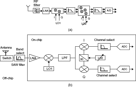
Figure 4.18 (a) Wide-IF RF converter and (b) on-chip implementation of wide-IF receiver
This approach is similar to a superheterodyne receiver architecture in that the frequency translation is accomplished in multiple steps. However, unlike a conventional superheterodyne receiver, the first local oscillator frequency translates all of the received channels, maintaining a large bandwidth signal at IF. The channel selection is then realized with the lower frequency tunable second LO. As in the case of direct conversion, channel filtering can be performed at baseband, where digitally programmable filter implementations can potentially enable more multi-standard capable receiver features.
In contrast to the previous architectures, the first local oscillator frequency is fixed. All available channels are converted into an intermediate frequency, resulting in a wide bandwidth at IF. Up-converted frequency components are removed by a simple low-pass filter. Channel selection and filtering are done at IF. Owing to the lower operation frequency, the requirements for the tunable LO and low-pass filter in the second down-conversion stage are relaxed. Hence, a narrow channel can be selected and filtered without off-chip components. Furthermore, filtering can be performed partly in the digital domain, which adds to multi-standard operation capabilities of this architecture. This flexibility comes at the expense of higher linearity requirements of the ADC.
The wideband IF architecture offers two potential advantages with respect to integrating the frequency synthesizer as compared with a direct conversion approach. The foremost advantage is the fact that the channel tuning is performed using the second lower frequency, or IF, local oscillator and not the first, or RF, synthesizer. Consequently, the RF local oscillator can be implemented as a fixed-frequency crystal-controlled oscillator, and can be realized by several techniques that allow the realization of low-phase noise in the local oscillator output with low-Q on-chip components. One such approach is the use of wide phase-locked loop (PLL) bandwidth in the synthesizer to suppress the VCO contribution to phase noise near the carrier. Note that the VCO phase noise transfer function has a high-pass transfer function close to the carrier and the bandwidth of suppression is related to the PLL loop bandwidth. In addition, as channel tuning is performed by the IF local oscillator, operating at a lower frequency results in a reduction in the required divider ratio of the phase-locked loop necessary to perform channel selection. The noise generated by the reference oscillator, phase detector, and divider circuits of a PLL all contribute to the phase noise performance of a frequency synthesizer. With a lower divider ratio, the contribution to the frequency synthesizer output phase noise from the reference oscillator, phase detector, and divider circuits can be significantly reduced. Moreover, a lower divider ratio implies a reduction in spurious tones generated by the PLL. An additional advantage associated with the wideband IF architecture is that there are no local oscillators operating at the same frequency as the incoming RF carrier. This eliminates the potential for the LO re-radiation problem that results in time-varying dc offsets. Although the second local oscillator is at the same frequency as the IF desired carrier in the wideband IF system, the offset that results at baseband from self mixing is relatively constant and is easily cancelled.
As the first local oscillator output is fixed and is different from the channel frequencies, the problem of dc offset is alleviated in the wideband-IF architecture. The still existing self-mixing in LO1 or LO2 results in constant dc offsets that can be removed either in the analog or digital domain. Isolation from the channel selection oscillator (LO2) to the antenna is much larger than in the heterodyne case. This greatly reduces problems associated with time varying offsets. Using a fixed frequency at LO1 allows for phase noise optimization for this oscillator. Frequency conversion into IF introduces images again. These can be removed using a Weaver architecture, but mismatches between the I and Q paths limit the image suppression.
Also, additional components from the second conversion stage inevitably result in larger power consumption. These problems are balanced by good monolithic integration capabilities and improved multi-standard prospects due to programmable filtering in the DSP.
4.3.4.1 Advantages
(1) Allows for high level of integration, (2) relaxed RF PLL specification, VCO could be made on chip, (3) channel selection performed by IF PLL lower the required divider ratio, (4) good multi-standard ability, and (5) alleviated dc offset problem.
4.3.4.2 Disadvantages
(1) Increase of 1 dB compression point for the second set of the mixer, and (2) increased ADC dynamic range requirement because of limited filtering in comparison with the heterodyne receiver.
Applications – Feasibility has not been proven for GSM, but can be used in satellite radio receivers.
4.4 Receiver Performance Evaluation Parameters
Optimizing the design of a communications receiver is inherently a process of compromise. There are several factors that govern the performance of a radio receiver:
- Selectivity and Sensitivity: The most important characteristics of a receiver are its sensitivity and selectivity. Sensitivity expresses the level of the smallest possible input signal that can still be detected correctly (that is, within a given BER). Selectivity, on the other hand, describes the receiver's ability to detect a weak desired signal in the presence of strong adjacent channels, so called interferers. Thus, sensitivity is the lowest signal power level that the receiver can sense and selectivity is the selection of the desired signal from the many (which are received by the antenna). For a good receiver the selectivity and sensitivity should be higher than the reference level.
- Noise Figure (NF): Indicates how much the SNR degrades as a signal passes through the system. Low NF enables successful reception, even for low levels of received signal power.
The equation which relates the noise figure and sensitivity is as below:
where
S = sensitivity in watts
F = numeric system noise figure
B = receiver bandwidth in Hz
k = Boltzman's constant = 1.38 * 10−23 J/K
T0 = 290 Kand
S0/N0 = receiver's output SNR (numeric)
- Image Rejection (IR): Measures the ratio of the desired signal to the undesired image. The higher the IR the better the receiver.
- Phase Noise: Phase noise describes an oscillator's short-term random frequency fluctuations. Noise sidebands appear on both sides of the carrier frequency. Typically, one sideband is considered when specifying phase noise, thus giving single sideband performance. Thus, low phase noise is crucial for oscillators in receiver systems.
- Receiver Non-linear Performance: Amplifiers usually operate as a linear device under small signal conditions and become more non-linear and distorting with increasing drive level. The amplifier efficiency also increases with increasing output power, thus, there is a system level trade-off between the power efficiency or battery life and the resulting distortion. It is desired that the receiver's non-linear performance should be good.
- Processing Power to Drive Different Applications: A higher MIPS is always desirable to drive the different complex processings but there should be a trade-off between cost and power consumption.
- Cost and Size: This is the driving factor that is most required for design.
- Complexity: The implementation of receiver architecture should be simple.
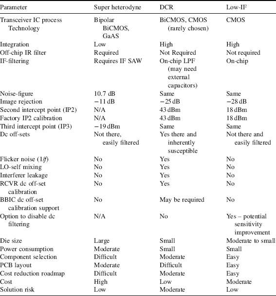
4.4.1 Receiver Architecture Comparison
The parameters for various receiver architectures are compared in the Table 4.2.
4.5 Transmitter Front-End Architecture
As discussed in the first section, the RF transmitter module mainly consists of a root raised cosine filter, modulator, power amplifier, RF filter, duplexer, and antenna.
4.5.1 Power-Limited and Bandwidth Limited Digital Communication System Design Issues
Communication system design involves trade-offs between performance and cost. Performance parameters include transmission speed, accuracy, and reliability, whilst cost parameters include hardware complexity, computational power, channel bandwidth, and required power to transmit the signal. Generally, a communication system is designed based on the criteria:
- bandwidth limited system
- power limited system.
Table 4.2 Receiver architecture comparison
In bandwidth limited systems, spectrally efficient modulation techniques can be used to save the bandwidth at the expense of power, whereas in power limited systems, power efficient modulation techniques can be used to save power at the expense of the bandwidth. In a system that is designed to be both bandwidth and power limited, error correction coding (channel coding) can be used to save power or improve error performance at the expense of bandwidth. Trellis coded modulation (TCM) schemes can also be used to improve the error performance of bandwidth limited channels, without an increase in bandwidth.
Generally, there are two main causes of error in a communication system: noise and distortion. We will first just consider distortion as noise was discussed in Chapter 2. The distortion occurs in an ideal baseband channel, only if the bandwidth of the transmitted signal exceeds the bandwidth of the channel and also at the transmitter's power amplifier module.
In order to come up with a proper design trade-off between accuracy, transmitted power, and transmission speed or bandwidth requirement, we need to examine how the energy of the baseband data pulse is distributed throughout the frequency band. The time and frequency band representations of single rectangular pulses of height A and width τ, is shown in the Figure 4.19.

Figure 4.19 Rectangular pulse, its frequency domain representation and power spectral density
From this, we can calculate and plot an average normalized power spectral density for a series of n number of such pulses as shown in Figure 4.20 and its value will be:

Figure 4.20 Power spectral density of n rectangular pulses
From Figure 4.20, it is obvious that most the power lies in the main lobe and inside the calculated BW. We can quantify the accuracy of the received signal for an ideal baseband channel by stating the percentage of the transmitted signal's power that lies within the frequency band passed by the channel. From Equation 4.2, it is evident that the accuracy (which is dependent on the transmitted power spectral density G(f) at a pre-defined label), bandwidth or speed of transmission (τ) and the amplitude of the data pulse are interdependent. This indicates that if the transmission rate is more, which requires more bandwidth, then to keep the accuracy at the same label (for example, 95%), we need to increase the amplitude or power level of the data pulse and vice versa. More BW means more average transmitted power will lie inside the frequency band, so the amplitude of the signal A (for example, transmitted power level) can be reduced. Thus more available BW requires less transmitted power for the same level of accuracy (desired power in the selected band).
If we increase the amplitude of the pulse, this will lead to more power consumption, more interference, and more non-linear distortion in the amplifier. Hence we need to investigate how we can increase transmission speed without reducing accuracy or increasing the bandwidth and amplitude of the transmitted pulse. Special shaped pulses, which require less bandwidth than rectangular pulse need to be considered. We know that bandwidth is inversely proportional to pulse width τ and we want the pulses to be as wide as possible to reduce bandwidth, but we do not want the pulses to overlap. This is accomplished by selecting a pulse width of τ = T, making each pulse as wide as its corresponding bit period. Thus we can relate the optimum pulse width and transmission speed by: τopt = 1/rb.
Our requirement should be: (1) a spectrally compact and smooth shaped pulse, as this will contain lower frequency components; and (2) the pulse transmitted to represent a particular bit should not interfere at the receiver with the pulse transmitted previously, for example, there should not be any inter symbol interference (ISI).
Keeping these two points in mind, the sync-shaped pulse in the time domain satisfies both the requirements. It is important to observe that there will be no ISI at exactly the center of each bit period. So at the receiver we need to sample the received signal exactly in the center of each bit period to avoid ISI. However, if the receiver is not completely synchronized with the transmitter, then this will cause timing jitter. Now the question is how we can reduce the timing jitter or ISI. This indicates we need to use a pulse that is smooth, like a sync pulse, but has a narrower main lobe and flatter tails. Consider the waveform as shown in Figure 4.21, which is a sync-shaped pulse multiplied by a damping factor, and is known as raised cosine pulse shape. The larger the damping factor β, the narrow the main lobe and the flatter the tail of the pulse. Thus a larger value of β means less effects of ISI and less susceptibility to timing jitter, but, greater the value of β, the greater is the bandwidth. The roll-off factor α = β/(rb/2) allows us to express the trade-off of additional bandwidth for less susceptibility to jitter in a manner that is independent of transmission speed.

Figure 4.21 Damped sync pulse
The trade-offs for selecting the pulse shapes for binary PAM is shown Table 4.3.
Table 4.3 Advantages and disadvantages of using different pulse shapes

Obtaining tighter synchronization requires more complex equipment within the receiver, thus transmitting raised cosine pulses will reduce the receiver's complexity relative to transmitting sync pulses. A filter, composed of discrete components, is designed to produce an impulse response resembling a time delayed version of the raised cosine pulse. Then a series of narrow pulses are input to the filter, one pulse per bit period, with a positive narrow pulse representing each “1” whereas a negative narrow pulse represents each “0.” The drawback of the analog method is it requires large numbers of discrete components.
Generating raised-cosine shaped pulses using digital circuitry is much easier than using analog circuits. As we have observed, these design parameters such as accuracy, transmitted power, BW, data rate, and complexity are all inter-related and hence the proper trade-offs depend on system's application.
4.5.2 Investigation of the Trade-offs between Modulation and Amplifier Non-Linearity
The choice of modulation has always been a function of hardware implementation, and required modulation and BW efficiency. Amplifiers usually operate as a linear device under small signal conditions and become more non-linear and distorting with increasing drive level. The amplifier efficiency also increases with increasing output power, but this leads to the problem of increased non-linear distortion and reduced battery life. For most commercial systems, this trade-off is constrained by interference with adjacent users, power efficiency, battery life, and resulting signal distortion. Thus, in many cases the amplifier signal levels are reduced or “backed off” from the peak efficiency operating point. Hence, we need to investigate the amplifier–modulation combination to minimize the energy required to communicate information.
Linear transmitter power amplifiers, such as class-A or class-B type of amplifiers, offer good quality, low output signal distortion but with significant penalties in heat dissipation, size, and efficiency. Alternatively, non-linear amplifiers such as class-C amplifiers offer very good efficiency and low heat dissipation but introduce more distortion into the output signal. As the class-C and -AB type of amplifiers offer good efficiency so, for better power usage purposes, this type of amplifier is generally used as the RF transmitter power amplifier.
A higher level of modulation states is used to carry more information bits per symbol. However, every time a modulation level is doubled an additional 3 dB of signal energy are needed to maintain the equivalent demodulator bit error rate performance.
For GSM, the modulation used is GMSK, where the filtering ensures the modulation is a constant envelope, the disadvantage is that decision points are not always achieved, resulting in residual demodulator bit error rate. TDMA systems have always required close control of burst shaping, the rise and fall of the power envelope either side of the slot burst. In GPRS this process has to be implemented on multiple slots with significant variations in power from burst to burst. As OFDM shows how highly sensitive it is to non-linear effects, so it requires more linear amplification than other modulation schemes. A multi-carrier modulated signal has a very large peak power, so the influence of the non-linear amplifier becomes large. Increase in peak power leads to input signal saturation, which leads to non-linear amplitude distortion and this leads to out of band radiation and degradation of BER.
The modulation schemes used for WLAN, UMTS, and GSM can be broadly divided into two categories.
4.5.2.1 Constant Envelope (Non-Linear) Modulation
In this case the signal envelope is fixed. It employs only phase information to carry the user data, along with a constant carrier amplitude. This allows the use of non-linear amplifier stages, which can be operated in class-AB or -C, so good power efficiency can be achieved. The most common standard employing non-linear modulation is GSM (Global Standard for Mobile Communication), which uses Gaussian minimum shift keying (GMSK) with a BT factor of 0.3 and raw data rate of 270.833 kbps.
4.5.2.2 Non-Constant Envelope (Linear) Modulation
In this case the signal envelope varies with time. The user information is conveyed in both the phase and amplitude of the carrier. Thus the transmitters should not distort the waveform at all, and hence amplifier stages must be operated in a linear class-A fashion. QPSK and BPSK are the modulation types used for the UMTS and WLAN OFDM systems. This means, WLAN and UMTS use non-constant envelope (linear) modulation whereas GSM uses a non-linear or constant envelope modulation scheme.
In the case of a multi-mode system, the modulation schemes for different modes are already defined. Therefore we have no scope to change the modulation scheme. However, we can come up with a best suitable transmitter architecture and power amplifier for this multi-mode terminal solution.
4.6 Transmitter Architecture Design
Transmitter design has unfortunately not resulted in a single preferred architecture suitable for all applications, due to the differing requirements for linear and non-linear modulation schemes.
4.6.1 Non-Linear Transmitter
The favored architecture for a constant-envelope transmitter is the offset phase-locked loop. This utilizes an on-frequency VCO, which is modulated within a phase-locked loop. A block diagram of this architecture is shown in Figure 4.22.

Figure 4.22 Transmitter architecture for non-linear modulation schemes
A modulated carrier is generated at an IF of f1 using an I–Q vector modulator. The modulated carrier is applied to the phase-locked loop, which modulates the VCO phase in order to track the phase of the feedback part of the phase comparator. The output signal fout is converted back down to f1 using a mixer with an LO at f2 such that f1 = fout − f2, for comparison in the phase detector.
This architecture is used in most of the current GSM phones, as it provides optimum power efficiency, cost, and performance by minimizing the amount of filtering required at the output. It also readily extends to future GPRS enhancements. The offset approach eliminates the problems of LO leakage, image rejection, and spurious sideband conversion associated with heterodyne architectures, reducing the filtering requirements at the PA output. The PLL has a low-pass response to the vector modulator, which invariably has a high wideband noise floor. The noise is therefore rejected by the loop before the signal reaches the PA. The output is also protected from the high noise figure of the offset mixer, which is not the case in heterodyne architectures. As the signal is of constant amplitude, it is possible to apply power control within the power amplifier stages, which follow. This allows the main transmitter to be optimized for power consumption.
4.6.2 Linear Transmitter
Linear modulation transmitters are required to preserve both the phase and amplitude of the signal. The consequence of this is that the offset phase-locked loop transmitter cannot be used as it only transmits phase information. It would be possible to apply the amplitude modulation component at the VCO output, but there are technical difficulties associated with this technique, in particular AM-to-PM conversion in the power amplifier, which have yet to be solved to give a viable solution. Instead a conventional heterodyne architecture is usually employed, comprising an IF modulator and an up-conversion mixer.
The power control requirements of the standards, usually call for power control to be distributed through the transmitter module. This is because the required dynamic range requires more than one variable gain stage. For a cellular system the final transmit carrier frequency can be up to 2 GHz. Variable gain amplifiers at the final transmit frequency are difficult to implement with large gain control ranges. Thus it is necessary to perform some of the gain control earlier in the transmitter chain.
The transmitter architecture for a linear scheme is shown in Figure 4.23. With the offset PLL architecture, the carrier modulation is achieved at an IF f1. Here the baseband I and Q signals contain information in both phase and amplitude. The signal is band-pass filtered to remove unwanted products and wideband noise from the vector modulator output, and a variable gain stage enables some power control (subject to carrier leakage limitations). This signal is then up-converted in a mixer using an LO at frequency f2. The output is filtered for image rejection, and so on, and a further variable gain stage is used to give the total required dynamic range. The distribution of the power control needs to be carefully planned to maintain the SNR along the chain. In particular, the vector modulator and up-convert mixer generate wideband noise levels, which need to be considered in the transmitter level plan. The subsequent power amplifier is required to be linear for the entire dynamic range of the transmitter, which can lead to power inefficiency. However, some transmitters do switch the PA bias from high to low power, to help this situation.

Figure 4.23 Transmitter architecture for linear modulation schemes
4.6.3 Common Architecture for Non-Linear and Linear Transmitter
The future of wireless communication can be considered as a plethora of heterogeneous systems operating together with current and legacy technologies. A mobile handset designed to operate on multiple RF bands is called multi-band phone and when it is designed to operate for different cellular standards it is called multi-mode phone. One viewpoint of the next generation wireless communication is the seamless integration of a wide variety of systems (cellular – GSM, GPRS, EDGE, UMTS, and WLAN) for efficient service provision. WLAN handsets offer a significant improved data rate over cellular handsets. However, they have a very limited range and access nodes can only be found in high use areas. On the other hand, a cellular handset, which has a larger range at the expense of data rate, can solve this problem of insufficient range. For cellular handsets, several standards have been introduced, which will co-exist. Also, various frequency bands have been introduced at different geographical locations. So one major challenge will be to find a robust solution to incorporating both WLAN and different cellular modes (GSM-900/1800 and UMTS) into single user terminal equipment (UE), which should have the capability to select the appropriate mode in any given coverage area available, ideally with a seamless interface between the different modes of operation.
For each standard, the handset must be able to transmit and receive with conformity to the ANSI/IEEE or 3GPP standard. The Table 4.4 tabulates different parameters used for different modes of operation. A number of issues arise when so many functionalities for different standards co-exist in small single user equipment, but we will mainly focus on the transmitter design challenges.
Table 4.4 Use of various modulation techniques for different systems

Unfortunately, conventional GSM/GPRS transmitter architectures are designed to deliver constant-envelope half-duplex signals and have little in common with UMTS architectures, which generate envelope-varying full-duplex signals. As a result, combining these transmitters within one multimode handset can be an expensive proposition. However, by changing the transmitter's modulation system from quadrature (I–Q) to polar, the architectures can be designed to deliver constant-envelope and envelope-varying signals. Polar transmitter-based architectures have no requirement for linear radio-frequency (RF) circuitry, which means that circuits can be designed with an emphasis on optimizing efficiency rather than linearity.
This describes a new architecture for implementing multi-mode multi-band transmitters, which provides all the necessary functionality for both linear and non-linear modulation schemes. There are a number of different architectures that can be employed to implement a multi-mode transmitter. However, the trade-offs between power consumption, linearity, baseband complexity, and implementation issues have resulted in a favored architecture for supporting both non-linear and linear modulation. In Figure 4.24, the architecture of a multi-mode transmitter supporting the linear and non-linear modulation scheme is shown.

Figure 4.24 Multi-mode linear-nonlinear transmitter
As discussed there are several problems associated with the power amplifier design, and below some advantages and disadvantages of using a direct conversion linear transmitter are indicated.
Advantages: (1) The circuit BW should not exceed the signal BW. (2) Wide output power dynamic range. (3) No problem if the RF signal amplitude becomes zero. (4) There is wide experience in design and manufacturing. (5) Generally it supports any signal type.
Disadvantages: (1) RF circuits are generally not linear leading to compensating design complexity. (2) Low dc to RF energy efficiency due to back off requirement. (3) High PA operating temperature from internal power dissipation. (4) High broadband output noise floor. (5) Difficulty maintaining modulation accuracy. (6) The possibility of self-oscillation. (7) Gain that is dependent on frequency.
To address the PA efficiency problem with envelope varying signals, polar modulation techniques were proposed.
4.6.4 Polar Transmitter
The polar transmitter transforms the digital I–Q baseband signals from the Cartesian domain to the polar domain. The quadrature equivalent signal representation is: S(t) = I(t) cos ωct + Q(t) sinωct, which can be represented in the polar domain as A(t) cos [ωct + Φ(t)]. In this case the amplitude and phase components of the signal are processed independently. The phase information extracted from the original signal (either constant envelope or non-constant envelope) is transformed into a constant envelope signal. This is achieved by phase modulating with the help of a phase lock loop designed to output the desired transmit frequencies. The resulting signal may now be amplified by compressed amplifiers without any concern of distorting the amplitude information.
The extracted amplitude information is quantized into control bits. These bits are used to modulate a digital power amplifier (DPA). Each bit is a digital representation of the amplitude envelope. The control bits are used to switch amplifier elements of the DPA into on or off states. The examples use a 7-bit control word offering 128 unique amplitude modulation states. Fewer quantization states can be implemented if decreased amplitude modulation resolution is acceptable. More quantization states can also be implemented for greater resolution. The digitized amplitude envelope and the phase-modulated RF carrier are synchronized and recombined within the DPA to produce linear and efficient RF transmission. Existing developments of polar modulated transmitters generally fall within three major categories: polar loop, polar modulator, direct polar.
Polar Loop: Feedback control is used to correct the output signal into its desired form (Figure 4.25). One advantage of such a polar loop is improved PA efficiency over the best linear systems, gained from operating the power amplifier much closer to saturation. Additional benefits from this compressed PA operation include a low wideband output noise floor and also usually a reduction of circuit oscillation tendencies with varying output load impedance. Disadvantages include the need for a precision receiver within the transmitter, control loop bandwidths which must greatly exceed the signal bandwidth, restricted output power dynamic range, maintaining stability of the feedback control loops across the output dynamic range, and the lack of circuit design techniques when operating with strong circuit non-linearity.

Figure 4.25 Polar loop transmitter

Figure 4.26 Polar modulator transmitter
Polar Modulator: As shown in Figure 4.26, in this type of transmitter, the output signal is amplified from the output of this polar modulator using conventional linear amplifier devices. The advantages and disadvantages of the polar modulator transmitter are given in Table 4.5.
Table 4.5 Advantages and disadvantages of polar modulator transmitter
| Advantages | Disadvantages |
| The modulator noise is much lower than a quadrature modulator | Linear PA provides no efficiency benefit |
| Pre-distortion applied to the polar modulator | Time alignment of amplitude modulation and phase modulation is required |
| Generating output power = 0 is not an issue | Lack of manufacturing experience for polar modulator transmitter |
| Sigma-delta ADC can be used along with this | |
| Modulation accuracy is good |
Direct Polar Transmitter: Another method that removes the feedback from the PA is a direct polar transmitter. This is shown in Figure 4.27. The advantages and disadvantages of the direct polar transmitter are shown in Table 4.6.
All signals have constant-envelope phase components, so linear RF circuitry is not required in either architecture. Between the UMTS and GSM modes, most of the things are implemented digitally within the polar modulator, and therefore have little impact on how the radio design is actually implemented.

Figure 4.27 Direct polar transmitter
Table 4.6 dvantages and disadvantages of a direct polar transmitter
| Advantages | Disadvantages |
| Efficiency is higher than the best linear transmitter | Power amplifier (PA) characterization required within the transmitter |
| Linear RF circuit is not required | AM/AM and AM/PM distortion |
| Unconditional power amplifier stability | Time alignment of AM and PM paths |
| Modulation accuracy | Lack of manufacturing experience |
4.7 Transmitter Performance Measure
The performance of a transmitter is generally measured taking the following factors into account: amplifier power efficiency, amplifier non-linear distortion, modulated signal power efficiency, and signal bandwidth efficiency. This is based on the total energy needed per transmitted bit, and bandwidth efficiency.
The average total power consumed by the amplifier is:
where
Pae = the instantaneous power-added efficiency of the amplifier
Pae(t) = [Prf(t) − Pin(t)]/Pdc(t)
Transmitter figures of merit are dependent on the following parameters: (1) spectral efficiency, (2) power efficiency, (3) spurious emission, and (4) power level.
4.7.1 Design Challenges
Transmitter architectures for multiple standards include direct up-conversion, translation loop, modulation through a phase-locked loop and a polar loop. The trend has been towards further digitizing to reduce the analog content in the total transmitter chain. Key challenges include current drain, dynamic-range requirements, and cost. Loop-phase modulation using a sigma-delta modulator shows promise in terms of low power consumption and a simpler architectural approach. For systems such as CDMA and W-CDMA, separation of AM and PM components is required. This leads to polar loop architectures, which are gaining wider use. However, challenges remain in their use for wideband systems, where alignment of the AM and PM components and the effect on spectral distortion are critical. While direct modulation has the advantage of compatibility with multiple standards, the challenges of meeting noise-floor requirements remain. Multimode phones require several bulky SAW filters to attenuate the received band noise. Signal digitization in the transmitter could include I and Q over-sampled D/A converters to ease the requirements of the reconstruction filter. As there are no blockers in the transmitter, this eases the design of the converter somewhat. Sufficient dynamic range to meet spectral mask requirements still has to be considered in the transmitter chain.
The final stage in the transmitter chain is the power amplifier, which transmits close to 3 W at maximum output power in certain systems. Maintaining efficiency at such power is critical; traditionally, PAs have been designed in GaAs or InGaP.
Recent trends point toward CMOS power amplifiers that can potentially enable on-chip integration with the rest of the transmitter and lower system costs. However, challenges remain in terms of efficiency, thermal behavior and isolation.
Further Reading
Das, S.K. (2000) Microwave Signals and Systems Engineering, Khanna, New Delhi.
Stern, H.P.E. and Mahmoud, S.A. (2004) Communication Systems: Analysis and Design, Pearson Education, Upper Saddle River, NJ.
Varrall, G. and Belcher, R. (2003) 3G Handset and Network Design, John Wiley Publishing, Hoboken.