3
Molecular Technology for Organic Semiconductors Toward Printed and Flexible Electronics
Toshihiro Okamoto1,2
1 Graduate School of Frontier Sciences, Department of AdvancedMaterials Science, The University of Tokyo, 5-1-5 Kashiwanoha, Kashiwa, Chiba, 277-8561, Japan
2 Precursory Research for Embryonic Science and Technology (PRESTO), Japan Science and Technology Agency (JST), 4-1-8 Honcho, Kawaguchi, Saitama, 332-0012, Japan
3.1 Introduction
Organic semiconductors are of scientific and technological interest because of their potential utilization in printable and flexible electronic applications such as organic field‐effect transistors (OFETs) [1], organic light‐emitting diodes (OLEDs) [2], and organic photovoltaic cells (OPVs) [3]. The functions of organic semiconductors are generated by intermolecular charge transport between their constituent neighboring π‐conjugated molecules and the geometric and energetic features of which essentially determine the device performance [4–6]. Therefore, versatility in material design offers enormous possibilities in building the molecules desired for organic semiconductors, which would facilitate the initiation of practical industrialization.
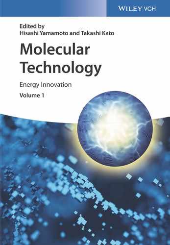
The general requirements for printed and flexible electronic applications are as follows: (i) high chemical stability under ambient condition (toward oxygen and water), (ii) high carrier mobility (exceeding the performance of conventional amorphous silicon semiconductors (0.5–1.0 cm2 V−1 s−1) and to compete with metal‐oxide semiconductors), (iii) enough solubility in common organic solvents for the achievement of low‐cost solution process technology, and (iv) high thermal durability (highly stabilized crystal phase above at least 150 °C to survive the device fabrication processes, such as curing metallic paints or sealing, for completing such products as display panels) [7]. Essentially, the stability of aggregated form against thermal stress and molecular thermal motion is an indispensable requirement for intermolecular charge transport because the highly fluctuating position of each molecule is similar to the situation in disordered molecular systems [8], where fundamental electronic coherence can be destroyed [9]. Furthermore, in the viewpoint of plant scalability for organic semiconductors, a low‐cost and environmentally friendly synthetic route is also required in the future (Figure 3.1).
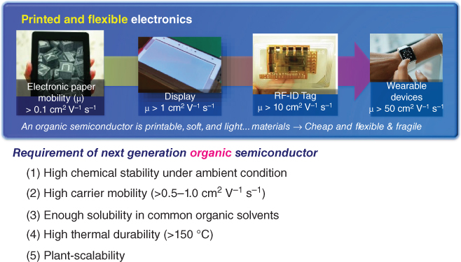
Figure 3.1 Requirements of the next‐generation organic semiconductor.
To develop applicable organic semiconductors, many researchers with various approaches based on their own molecular designs focus on the aforementioned requirements. A great number of organic semiconducting materials based on π‐electron‐conjugated molecules such as linear and quasilinear acenes and heteroacenes composed of benzene‐ and/or heterole π‐electronic cores (π‐cores) have been extensively studied and developed for such applications. Additional features such as luminescence [10] and sensing [1, 11] are fascinating characteristics of organic semiconductors and have been the focus areas in recent research.
This chapter focuses on the historically important small molecular‐type semiconducting π‐cores, such as acenes, heteroacenes, and the other promising and high‐impact organic semiconducting molecules of hole‐ (p‐type) and electron‐ (n‐type) transport characteristics based on “molecular technology.” Furthermore, the chapter also describes the achievement to the transistor performance of organic semiconductors in polycrystalline‐ and single‐crystalline‐based devices along with recently developed solution process technique.
3.2 Molecular Design and Favorable Aggregated Structure for Effective Charge Transport of Organic Semiconductors
In an organic semiconductor consisting of the weak intermolecular interactions such as van der Waals force, charge carriers travel through the overlap of π‐orbitals of neighboring molecules, whereas through covalent bonds in an inorganic semiconductor. Therefore, the aggregated structure is crucial to effective charge transport. Considering that an organic semiconducting molecule has π‐conjugated skeletons such as benzene and heterole rings, an organic material shows aggregated structures classified to one‐dimensional (1D) and two‐dimensional (2D) structures, as shown in Figure 3.2. From the theoretical investigation, charges would transport more effectively in 2D aggregated structures such as herringbone and brick‐work packing than in 1D structures such as a π‐stacking. In the case of herringbone and brick‐work packings, one molecule is surrounded by other six and four molecules, which correspond to the effective orbital overlap (transfer integral, t) among the six and four molecules, respectively. On the other hand, in the case of the π‐stacking, one molecule is surrounded by only two molecules. It is considered that 2D structure is preferable to 1D structure because a real material solid includes unavoidable defects or contaminations preventing orbital overlaps. Thus, it is important to understand how to construct two‐dimensionally ordered aggregated structures, achieving organic semiconductors of high carrier mobility.
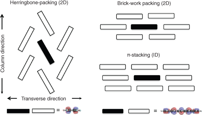
Figure 3.2 Herringbone packing (2D), brick‐work packing (2D), and π‐stacking (1D).
3.3 Molecular Design of Linearly Fused Acene‐Type Molecules
As organic semiconductors, various aromatic compounds have been investigated. Among them, linearly fused benzene ring systems, called “acenes”, such as naphthalene, anthracene, tetracene, and pentacene, are one of the most important and well‐studied organic semiconducting materials. As shown in Figure 3.3, acenes have shallow highest occupied molecular orbital (HOMO) levels depending on the number of fused rings, resulting in p‐type semiconducting behavior (hole transporting). As the HOMO levels of tetracene and pentacene are closer to the Fermi level of gold electrodes (−5.1 to −4.9 eV), holes can be smoothly injected into their HOMOs.
Figure 3.3 HOMO and LUMO levels of a series of acenes (HOMO and LUMO levels are calculated at B3LYP/6‐31Gd and B3LYP/6‐31Gd+ levels, respectively).
The aggregated structures of naphthalene [12], anthracene [13], tetracene [14], and pentacene [15] are summarized in Figure 3.4. Notably, all acenes form herringbone packing. These packings might be induced by the difference between the inner and outer electrostatic potential derived from the difference of the electronegativity of carbon and hydrogen atoms, called “C−H⋯π interaction” [16]. As is well known, benzene itself is aggregated to the face‐to‐edge forms by C−H⋯π interaction in single‐crystal state [17, 18]. Acenes, more than naphthalene, show two‐plane angles of 49.7° to 53.0° between neighboring molecules in crystal phase. The trend indicates that the balances between the inner and outer electrostatic potentials in the π‐core should play a role to form the 2D herringbone packing (according to detailed theoretical investigations, the dispersion interactions are major source of the attraction [19, 20]).
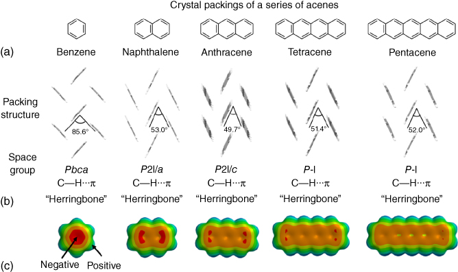
Figure 3.4 (a) Chemical structures of benzene, naphthalene, anthracene, tetracene, and pentacene. (b) Packing structures of these acenes along with their space group in single‐crystal structures. (c) Electrostatic potential maps of all acenes in the property range from −100 to +100 kJ mol−1 (calculated by SPARTAN 16 program).
Although early research on conductivity of naphthalene crystals were reported [21], tetracene and pentacene have been well studied as organic semiconductors in chemical, physical, or device engineering fields. In a polycrystalline thin film fabricated by vacuum deposition, tetracene and pentacene exhibited hole mobilities of 0.1 and 3 cm2 V−1 s−1, respectively [22, 23]. Compared with polycrystalline films having grain boundaries at which molecules misalign, single crystals could neglect such extrinsic factors to evaluate the intrinsic carrier‐conduction in organic semiconductors. Using single crystals grown by physical vapor transport technique [24, 25], the hole mobility of tetracene and pentacene in single‐crystal‐field‐effect transistors (SC‐FETs) is 1.4 [26] and over 10 cm2 V−1 s−1 [27, 28], which are apparently higher than those in polycrystalline field‐effect transistors (FETs). As the most promising tetracene derivatives, 5,6,11,12‐tetraphenyltetracene, called “rubrene”, whose aggregated structure is also in herringbone packing, exhibited an extremely high hole mobility of up to 40 cm2 V−1 s−1 in SC‐FETs [29], whereas the polycrystalline thin film of rubrene showed very low performance due to the possible difficulty of formation of oriented polycrystalline films.
3.4 Molecular Technology of π‐Conjugated Cores for p-Type Organic Semiconductors
Although tetracene, rubrene, and pentacene are the promising organic semiconducting materials, they are gradually decomposed under ambient condition [30]. Among them, pentacene has a shallow HOMO level of −4.60 eV and a highly reactive site at central 6,13 positions to easily convert the oxidized pentacene such as pentacene quinone. One of the solutions for overcoming this instability is a new π‐conjugated core based on molecular technology, as shown in Figure 3.5. First, Katz and Bao developed anthra[2,3‐b:6,7‐b′]dithiophene (ADT) and anthra[2,3‐b]thiophene (AT), and tetraceno[2,3‐b]thiophene (TT) as new stable π‐cores [31, 32], which were simply replaced with thiophene ring at the terminal benzene ring. ADT, AT, and TT have slightly deeper HOMO levels of −4.80, −4.98, and −4.70 eV, respectively, and show a substantial reduction of HOMO coefficient at certain reactive sites.

Figure 3.5 Historical molecular design of p‐type semiconductors: Chemical structures and HOMO of a series of acenes and heteroacenes.
Their aggregated structures form the herringbone packing similar to that of acenes, which results in a high hole mobility of up to 0.5 cm2 V−1 s−1 in vacuum‐deposited polycrystalline films [32]. These derivatives triggered the synthesis of thiophene and other heterole‐containing acenes, namely heteroacene [33]. As typical heteroacenes, the chemical structures and HOMO of bisthieno[2′,3′:4,5]thieno[3,2‐b:2′,3′‐d]thiophene ([5]TAc) and thieno[3,2‐b:4,5‐b′]bis[1]benzothiophene (DBTDT) are illustrated in Figure 3.5. The introduction of thiophene rings in the whole or central sites of molecules lead to the deeper HOMO levels of −5.30 and −5.54 eV for [5]TAc and DBTDT, respectively. Both molecules exhibit high chemical stability under ambient condition as well as thermal stability to easily purify them by sublimation. Their HOMO coefficients are located at the double bonds and benzene rings, are not located at the sulfur atoms. This trend is totally different from that of ADT, AT, and TT as described earlier. The packing structures of [5]TAc and DBTDT are shown in Figure 3.6. DBTDT has typical herringbone packing with the tile angle of 56.5° in C−H⋯π and S⋯π short contact. On the other hand, [5]TAc has 1D‐like herringbone packing (π‐stacking) with the large tile angle of 130° and S⋯S short contact. As described in the section of acenes, since [5]TAc does not have any hydrogen atoms at the molecular longitudinal site and good balance of electrostatic potential map, it prefers π‐stacking to herringbone packing. Furthermore, although [5]TAc has the attractive short contacts between sulfur atoms, no HOMO coefficient at sulfur atoms results in the small intermolecular electronic coupling, indicating that the column direction is well overlapped to give a large absolute transfer integral of 172 meV compared with the value of transverse direction of 2 meV. Thus, the behavior of DBTDT single crystals is 1D‐type charge transport characteristics. In the case of DBTDT, the absolute transfer integrals (11 and 17 meV) are somewhat small as shown in Figure 3.6 due to the same reason as the case of [5]TAc with no HOMO coefficient at sulfur atoms. The reported hole mobility of [5]TAc is 0.045 cm2 V−1 s−1 in polycrystalline thin films [34].
![(a) Chemical structures of [5]TAc, DBTDT, BTBT, and DNTT. (b) Packing structures of [5]TAc, DBTDT, BTBT, and DNTT along with the absolute transfer integral values in the direction of column and transverse and their space group in single-crystal structures. (c) Electrostatic potential maps of [5]TAc, DBTDT, BTBT, and DNTT in the property range from -100 to +150 kJ/mol.](http://images-20200215.ebookreading.net/4/1/1/9783527341634/9783527341634__molecular-technology-volume__9783527341634__images__c03f006.jpg)
Figure 3.6 (a) Chemical structures of [5]TAc, DBTDT, BTBT, and DNTT. (b) Packing structures of [5]TAc, DBTDT, BTBT, and DNTT along with the absolute transfer integral values in the direction of column and transverse and their space group in single‐crystal structures. (c) Electrostatic potential maps of [5]TAc, DBTDT, BTBT, and DNTT in the property range from −100 to +150 kJ mol−1 (calculated by SPARTAN 16 program).
To increase the intermolecular orbital overlap between neighboring molecules in the heteroacene system, the molecule having effective HOMO coefficients on sulfur atoms should be constructed based on molecular technology. Takimiya et al. have developed two terminal benzene‐fused thienothiophene, [1]benzothieno[1]benzothiophene (BTBT). BTBT exhibits the same electronic structure of the chrysene π‐core. Notably, unlike [5]TAc and DBTDT described above, the sulfur atoms have effective HOMO coefficient in BTBT (Figure 3.5). The crystal structure of BTBT [35] forms the typical herringbone packing exhibiting C−H⋯π, S⋯π, and S⋯S short contact at the same time. Other promising molecular technological approaches to enhance orbital coupling is to apply highly π‐extended molecules. The phenyl‐substituted BTBT (DPh–BTBT) [36] and the π‐extended naphthalene‐terminated thienothiophene, dinaphtho[2,3‐b:2′,3′‐f]thieno[3,2‐b]thiophene (DNTT), and others were also developed [37, 38]. BTBT and DNTT exhibit excellent chemical stability under ambient condition due to the low‐lying HOMO levels of −5.58 and −5.18 eV and form the typical herringbone packing with the tilted angles of 56.4° and 51.0°, respectively. Intermolecular electronic couplings of HOMO (transfer integral, t HOMO) based on the packing structure of DNTT had been evaluated using the Amsterdam Density Functional (ADF) program package [39–41]. Although the absolute transfer integral of DNTT in the column direction is 71 meV, which is fairly large compared with that of DBTDT, the values of DNTT in the transverse direction are 91 and 14 meV, which is an anisotropic transport character. Among them, DNTT have high carrier mobilities of 2.9 and 8.3 cm2 V−1 s−1 in polycrystalline and single‐crystalline thin films, respectively [37].
3.5 Molecular Technology of Substituents for Organic Semiconductors
3.5.1 Bulky‐Type Substituents
As described earlier, although pentacene exhibits hole mobilities of 1–3 cm2 V−1 s−1 in vacuum‐deposited polycrystalline films [42–46], it is instable under ambient condition due to the existence of the highly reactive site. Moreover, pentacene itself is insoluble in commonly used organic solvents, which makes it difficult to apply solution process to pentacene. To overcome its instability and insolubility issues, Anthony et al. developed the molecular design of the introduction of bulky‐type substituents [47–50] such as triisopropylsilylethynyl groups to the pentacene core at the central reactive position [47]. Furthermore, the electron‐withdrawing nature of the ethynyl substituent helps electronic delocalization, that is, stability of pentacene π‐core. The compound, called triisopropylsilylethynyl‐pentacene (TIPS‐Pen), was easily synthesized. TIPS‐Pen shows high chemical stability even in solution state due to the lower lying HOMO level (E HOMO = −5.1 eV, determined by cyclic voltammetry). It has high solubility in common organic solvents, resulting in purification by using column chromatography. Interestingly, TIPS‐Pen forms “brick‐work” packing as shown in Figure 3.7. As described in the previous section, this packing is expected as one of the two‐dimensional charge‐transporting systems because four molecules are located surrounding one molecule via effective π‐orbital overlaps. In fact, after Anthony's first paper has been published, the mobility of TIPS‐Pen was reported to be 0.18–11 cm2 V−1 s−1 using several solution processes. Very recently, a new solution process technique “shearing method” developed by Bao et al. induced the more favorable brick‐work packing, resulting in a much higher mobility of 11 cm2 V−1 s−1 [51, 52]. By means of the molecular technological approach, unexplored more π‐extended acene systems, hexacene and heptacene, bearing TIPSE substituents were studied as new field of chemistry [4, 53, 54]. Of course, the molecular technological strategy has been applied to use other heteroacenes such as ADT and TT. For example, triethylsilylethynyl‐substituted anthra[2,3‐b:6,7‐b′]dithiophene (TES‐ADT) was synthesized and also formed brick‐work packing, resulting that it shows more than 1 cm2 V−1 s−1 by a simple solution process technique [48].
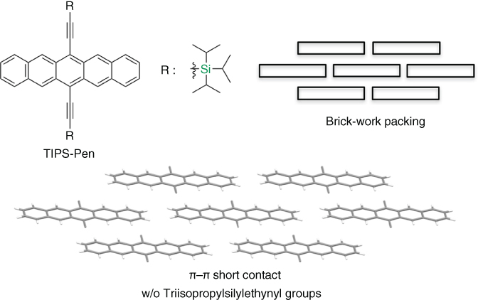
Figure 3.7 Chemical structures and packing structure of TIPS‐Pen. (Triisopropylsilylethynyl groups are omitted for clarify.)
3.5.2 Linear Alkyl Chain Substituents
The molecular design to produce solution‐processable organic semiconductors is the introduction of flexible and solubilizing long alkyl chains into the main π‐cores such as a small molecule and a polymer. In addition, such a long alkyl group can act as the driving force for molecular ordering in the solid state with the aid of the van der Waals intermolecular interaction between the alkyl chains. Thus, the long alkyl chains render the semiconducting core to pack tightly, enhancing charge‐transporting properties. Katz and coworkers first reported alkyl‐substituted ADT, which is soluble in toluene at room temperature, whereas ADT itself is not soluble in the same condition [31]. As other solution‐processable organic semiconductors, alkyl‐substituted BTBT (C n ‐BTBT) with different alkyl chains, from n‐C5H11 to n‐C14H29, were developed with a facile synthesis via two reaction steps using parent BTBT as a starting material. The aggregated structures of C8‐BTBT also form the typical herringbone packing with the tiled angle of 56.4°, C−H⋯π, and S⋯π short contacts in single crystal. C n ‐BTBTs exhibit excellent solubility in chloroform at room temperature and construct homogenous thin films by spin coating, whose mobility was higher than 10−1 cm2 V−1 s−1 in polycrystalline thin films [55]. To improve their charge carrier mobility and evaluate their intrinsic mobilities, the single‐crystalline films of C n –BTBT grown by several solution techniques exhibited a higher mobility of greater than 5 cm2 V−1 s−1 [56–58]. Furthermore, decyl‐substituted DNTT (C10‐DNTT) [59] as a π‐extended derivative also formed the herringbone packing and showed an excellent mobility of up to 11 cm2 V−1 s−1 in solution‐crystallized single‐crystalline thin films [60], whereas the solubility of C10‐DNTT is poor due to the highly π‐extension of the π‐core (Figure 3.8). Very recently, Hanna et al. developed asymmetrically substituted BTBT molecules, based on the molecular design for liquid crystals, exhibiting high carrier mobility by solution process as well as high thermal tolerability in devices [61].

Figure 3.8 (a) Chemical structures of C8–BTBT and C10–DNTT and (b) packing structures of C8–BTBT and C10–DNTT along with the absolute transfer integral values (t c and t t) in the direction of column and transverse and their space group in single‐crystal structures. n‐Octyl and n‐decyl groups are omitted for clarify.
3.6 Molecular Technology of Conceptually‐new Bent‐shaped π‐Conjugated Cores for p‐Type Organic Semiconductors
3.6.1 Bent‐Shaped Heteroacenes
As described in the previous section, to achieve effective charge transfer between neighboring molecules in organic semiconductors, it is likely to design the molecules with π‐extended electronic cores such as pentacene and DNTT. Introducing triisopropylsilylethynyl groups or long alkyl chains provided TIPS‐Pen, C n ‐BTBT, and C n ‐DNTT with solubility to result in solution‐processed crystalline thin films with excellent mobilities of greater than 10 cm2 V−1 s−1 [56, 58, 62–65]. Introduction of these substituents, however, gives instability of crystal phases because the molecular design of π‐cores with alkyl chains is similar to that for liquid‐crystal molecules. The stability of the thin films is relatively poor against temperature, and crystal phases of TIPS‐Pen, C n ‐BTBT, and C n ‐DNTT transit to liquid‐crystal phases at around 110–130 °C [55, 66, 67], resulting in the transistor performance degradation at a certain temperature or higher. These properties of the major organic semiconducting materials indicate that it is still difficult to achieve simultaneously sufficient solubility, thermal durability, and high‐mobility charge transport with the conventional molecular design strategy of π‐extended cores for organic semiconductors.
Recently, our group proposed a conceptually new molecular design of π‐extended V‐shaped conjugated cores, dinaphtho[2,3‐b:2′,3′‐d]thiophene (DNT–V) containing a thiophene ring at the central position. DNT–V exhibits inherent solubility because of intramolecular dipole moments and a large orbital coefficient of HOMO on the prominent sulfur atom, possessing potential for high mobility in the desired packing structure. Furthermore, the V‐shaped π‐core was expected to reduce molecular fluctuation to avoid fatally decreasing intermolecular transfer integrals because a bent molecular structure has larger steric hindrance than do straight π‐cores such as pentacene, BTBT, and DNTT that are easily imagined to rotate (Figure 3.9).
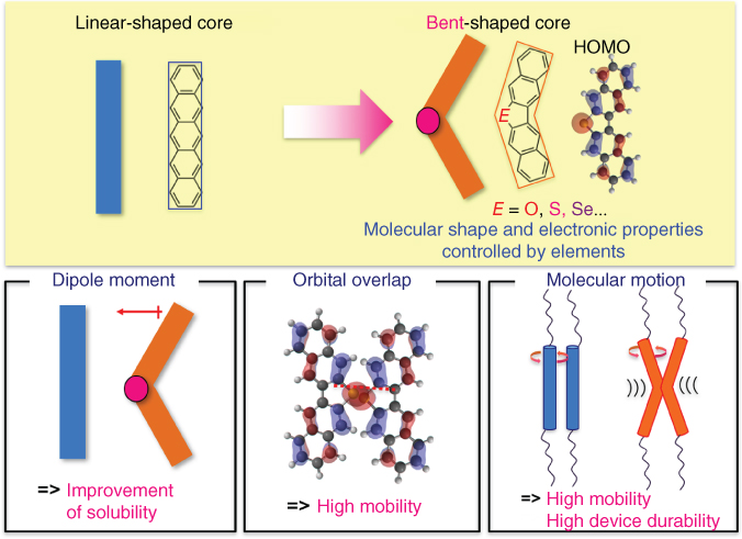
Figure 3.9 Molecular technology of bent‐shaped π‐electron cores.
A facile and versatile synthetic method for DNT–V and alkyl‐substituted derivatives was developed, in which vary the position and length of the alkyl chains attached to the core by four steps from commercially available starting materials without any expensive metal catalysts, indicating their advantageous capability of large‐scale production (Figure 3.10).

Figure 3.10 Reaction scheme of DNT–V, C n –DNT–VW, DNBDT–N, and C n –DNBDT–NW.
All derivatives have high chemical and thermal stability. Among them, notably, a series of C n –DNT–VW exhibits sufficient solubility in nonhalogenated solvents such as toluene and anisole at room temperature and very high phase‐transition temperatures of up to 202 °C. From the single‐crystal structural analysis of DNT–V derivatives, it is found that the unique “bent structures” induced by intermolecular interactions in the crystal and the resultant herringbone packing structure (Figure 3.11). Then, from the calculations of transfer integrals based on the actual single‐crystal structures, it was unveiled that the DNT–V derivatives realize effective two‐dimensional orbital overlaps in the herringbone packing (Figure 3.12). Their single‐crystalline films can be fabricated by a newly developed solution‐crystallization method to properly evaluate the carrier mobility of DNT–VWs in the single‐crystalline thin films without any influences from extrinsic and random grain boundaries [29, 68, 69]. Among the synthesized compounds, hexyl‐substituted DNT–V (C6–DNT–VW) shows a mobility of up to 9.5 cm2 V−1 s−1. Notably, the single‐crystal structural analysis and their transport characteristics of single‐crystalline films clearly demonstrated the correlation between the mobility and the transfer integrals as a result of good overlapping of the molecular packing geometry (Figure 3.11). Moreover, its transistors are thermally resistant at a temperature of up to 150 °C. This result is outstanding among reported high‐mobility organic semiconductors and is desirable for further practical device‐fabrication processes [7].
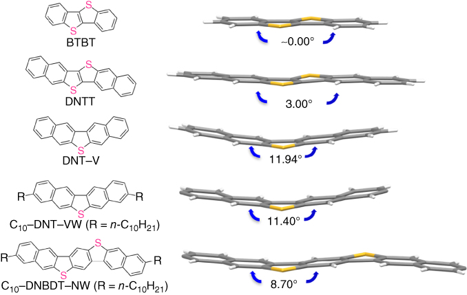
Figure 3.11 Molecular structures of DNT–V, C10–DNT–VW, and C10–DNBDT–NW compared with those of BTBT and DNTT in single crystals.
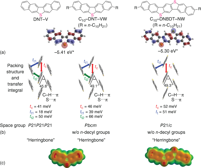
Figure 3.12 (a) Chemical structures of DNT–V, C10–DNT–VW, and C10–DNBDT–NW, and HOMO of DNT–V and DNBDT–N (R = H). (b) Packing structures of DNT–V, C10–DNT–VW, and C10–DNBDT–NW along with the absolute transfer integral values (t c, t t, t t1, and t t2) in the direction of column and transverse (transfer integrals were calculated at PBEPBE/6‐31Gd level) and their space group in single‐crystal structures. n‐Decyl groups are omitted for clarify. (c) Electrostatic potential maps of DNT–V and DNBDT–N in the property range from −100 to +150 kJ mol−1 (calculated by SPARTAN 16 program).
Although the highly potential sulfur‐bridged V‐shaped derivatives (DNT–V and C n –DNT–VW) have been developed, the following drawbacks of the DNT–V core still remain: (i) a large ionization potential (5.73 eV) of DNT–V because of deficient π‐conjugation length, resulting in a large absolute threshold voltage in the FET and (ii) a low molecular weight (MW) of DNT–V (MW 284) and a resultant low sublimation temperature, leading to unsatisfactory thermal durability in the form of thin films. Therefore, it is needed to further optimize the main π‐core. It was speculated that the molecular concept of the V‐shaped molecule could be extended to the N‐shaped molecular structure (N‐shaped π‐core), dinaphtho[2,3‐d:2′,3′‐d′]benzo[1,2‐b:4,5‐b′]dithiophene (DNBDT–N) and the alkyl‐substituted derivatives (C n –DNBDT–NW) (Figure 3.12). As expected, the ionization potentials of DNBDT and C10–DNBDT–NW (n = 10) are 5.45 and 5.24 eV, respectively, whose values are apparently improved because of the π‐extended core. In terms of thermal stability, the phase‐transition temperature of C10–DNBDT–NW from the crystal phase is evaluated to be greater than 200 °C. The single‐crystal structural analysis of the N‐shaped molecule, C10–DNBDT–NW, clarified the same attractive intermolecular interactions as C n –DNT–VW. Thus, the C10–DNBDT–NW molecule also showed the feature of energetically favorable bent structures (Figure 3.12) in single crystal. Although the unsubstituted DNBDT–N formed the unfavorable overlap in 1D π‐stacking, the simple introduction of long alkyl chains to DNBDT–N core can achieve a herringbone packing structure and effective intermolecular overlap by means of van der Waals interaction among long alkyl chains (Figure 3.12). Notably, solution‐crystallized FETs using C10–DNBDT–NW exhibited a mobility of up to 16 cm2 V−1 s−1. In addition, as a result of thermal stress tests for the solution‐crystallized FETs on polycarbonate substrates, its single‐crystalline film shows no obvious performance degradation even after annealing at 200 °C (Figure 3.13). Thus, these sulfur‐bridged V‐ and N‐shaped organic semiconductor materials, which are exceptional in satisfying the properties required for printed semiconductor devices, emerge as promising candidates for the printed and flexible electronics industries.
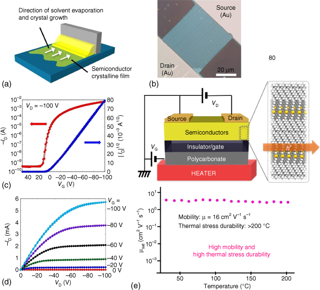
Figure 3.13 (a) Solution‐process image of edge‐casting method. (b) Solution‐crystallized films of C10–DNBDT–NW together with source and drain electrodes. (c and d) Transfer and output characteristics of the representative C10–DNBDT–NW solution‐crystallized transistor. (e) Thermal stress durability test of C10–DNBDT–NW solution‐crystallized transistor along with its molecular alignment and the device structure for the test.
Recently, furan, an oxygen‐containing congener, has been of particular interest because of its densely packed nature, which originates from a smaller element size [70–74]. Since such promising compounds were reported, furan‐based π‐conjugated systems have proved to be potential candidates as organic semiconductors. Our group reported oxygen‐incorporated congeners, dinaphtho[2,3‐b:2′,3′‐d]furan derivatives (DNF–Vs). Notably, alkyl‐substituted DNF–V derivatives (C n –DNF–VW), regardless of the positions of their substituents, exhibited a high hole mobility of greater than 1 cm2 V−1 s−1 in single‐crystalline thin films through edge‐casting [75]. Intriguingly, DNF–Vs show blue‐emissive characteristics with a high quantum efficiency (ΦF = 72%) even in the solid state [75, 76], whereas the sulfur‐bridged congener exhibits very weak photoluminescence with ΦF of lower than 3%. Single‐crystal analysis proved that all derivatives form a typical herringbone packing and good overlaps of the charge‐transporting π‐cores. These results indicate that an oxygen‐bridged V‐shaped π‐core is less susceptible to molecular displacement in an aggregated structure than its sulfur‐bridge counterparts, mainly due to its smaller element size. Furthermore, Okamoto et al. described an oxygen‐bridged N‐shaped π‐electron core, dinaphtho[2,3‐d:2′,3′‐d′]benzo[1,2‐b:4,5‐b′]difuran (DNBDF), as a new entity of organic semiconducting materials. Interestingly, by the introduction of flexible alkyl chains at appropriate positions, DNBDF π‐cores exhibit solution processability, a highly stabilized crystal phase, high mobility, and blue luminescence in a solid. Throughout this study, C10–DNBDF–NV exhibits a highly stabilized crystal phase up to 295 °C, blue emission with a moderately high quantum yield of 42%, even with flexible long alkyl chains in the solid state, and high carrier mobility of up to 1.8 cm2 V−1 s−1 in a solution‐crystallized FET [77]. Thus, DNF–Vs and DNBDF–Ns with both high‐efficient blue emission and high mobility are candidates for advanced light‐emitting transistors rather than simple FETs.
3.7 Molecular Technology for n‐Type Organic Semiconductors
n‐Type electron transporting organic semiconductors, needed for the function of complementary organic circuits, OPVs, and p–n junction diodes, exhibit challenges such as low mobility, instability in air, poor solubility for efficient film‐casting, and large barriers to electron injection with air‐stable electrodes such as gold. n‐Type semiconducting compounds are rarer than p‐type ones due to the nature of conventional π‐conjugated systems of the high‐lying lowest unoccupied molecular orbital (LUMO) levels. Therefore, the general molecular design of n‐type semiconductor is that acene, arylene, thiophene, and phenylene‐based π‐conjugated cores are functionalized with electron‐withdrawing substituents such as perfluoroalkyl, cyano, fluoro, perfluoroaryl, carbonyl, and diimide groups to delocalize electrons and yield stability and low‐lying LUMO [78, 79]. As representatively shown in Figure 3.14, naphthalene diimide (NDI), perylene diimide (PDI), and perfluoropentacene (F14‐Pen) functionalizing diimide and fluoro groups effectively have low‐lying LUMO levels of −3.77, −3.82, and −3.96 eV, calculated at B3LYP/6‐31Gd+ level, respectively. In this section of n‐type semiconductors, well‐investigated NDI and PDI‐based n‐type semiconductors and new promising n‐type benzobis(thiadiazole)‐based semiconductors are described based on the molecular design (Figure 3.15).
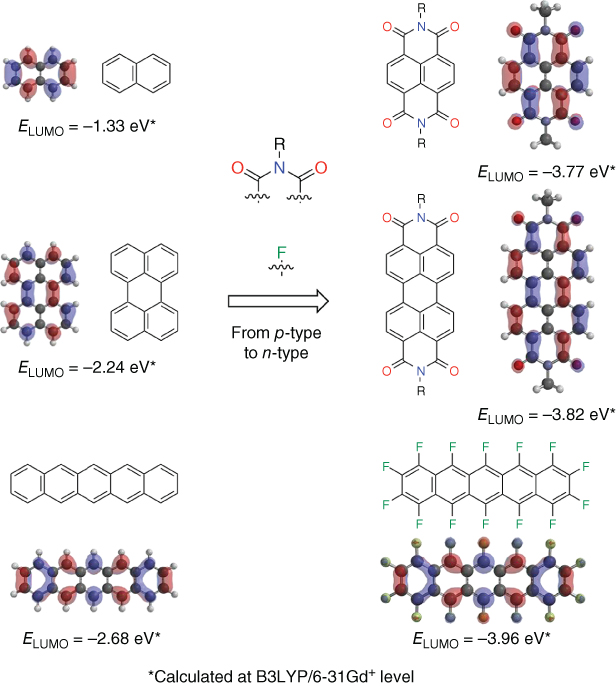
Figure 3.14 Molecular design of n‐type semiconductors: chemical structures and LUMO.
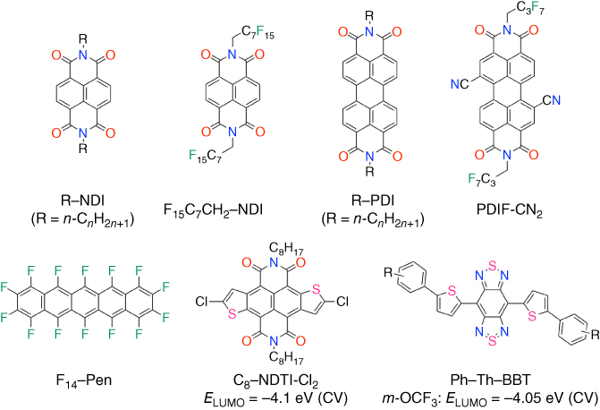
Figure 3.15 Chemical structures of representative n‐type semiconductors.
3.7.1 Naphthalene Diimide and Perylene Diimide
In terms of device durability under ambient condition, de Leeuw et al. first reported ambient stability in n‐type semiconductors in 1997 [80]. As degradation was attributed to the reaction of charge‐carrying electrons with oxygen and water, several strategies such as lowering LUMO levels of −4.0 eV or introducing physical oxygen/water barriers have been pursued to overcome these issues. Arylene with electron‐withdrawing diimide groups affords promising architectures. As one early example of arylene diimide, n‐fluoroalkyl‐substituted NDIs (F15C7CH2–NDI) exhibited air‐stable electron mobilities of up to 0.1 cm2 V−1 s−1 due to the presence of densely packed fluoroalkyl groups, whereas the LUMO level of NDI is higher than −4.0 eV. In sharp contrast, n‐alkyl‐substituted NDI‐based OFETs only operate under inert condition. This result clearly indicates that n‐fluoroalkyl groups act as a barrier to oxygen/water penetration [81, 82]. However, depending on the oxygen pressure and film morphology, some of these n‐fluoroalkyl‐substituted semiconductor‐based OFETs degrade over periods of days [83].
Facchetti, Marks, and coworkers demonstrated that functionalized arylene diimide cores with electron‐withdrawing substituents such as halogens and cyano groups result in highly electron‐deficient n‐type semiconductors having low‐lying LUMO levels and the packing structure favorable for charge transport [83]. Furthermore, very recently, 2,6‐dichloronaphthalene diimide was sublimed in air to give a new polymorph with the two‐dimensional brick‐work packing (β‐phase), whereas the herringbone packing motif (α‐phase) is grown from organic solvents in the previous report. Then, their single‐crystalline FETs based on α‐ and β‐phase crystals exhibit electron mobilities of up to 8.6 and up to 3.5 cm2 V−1 s−1, respectively [84].
Regarding π‐extended PDI derivatives, Horowitz et al. first reported the evidence for electron transport in PDI [85] and then Frisbie et al. reported structural and electrical transport properties of a family of π‐stacking soluble organic semiconductors, alkyl‐substituted perylene diimides (C n –PDI) [86]. OFETs based on C n –PDI‐deposited films showed electron mobilities of up to 1.7 cm2 V−1 s−1 in vacuum. The strategy of intrinsically air‐stable transistors against oxygen and water is realized to stabilize charge‐carrying electrons in low‐lying LUMO levels. Notably, PDI functionalized with cyano groups (PDIF–CN2) in the bay region exhibits highly air‐stable electron mobility of 0.64 cm2 V−1 s−1 [87]. The packing structure of PDIF‐CN2 forms the brick‐work packing exhibiting effective orbital overlaps that take advantage of the feature of the LUMO configuration (Figure 3.16). PDIF–CN2‐based transistors can be fabricated from vapor‐deposited and solution‐processed films [87]. Furthermore, its single‐crystal FETs were fabricated by lamination of the semiconductor crystal on Si–SiO2/PMMA‐Au gate‐dielectric‐contact substrates. PDIF–CN2 exhibits electron mobilities of up to 6 and 3 cm2 V−1 s−1 in vacuum and air, respectively [88].
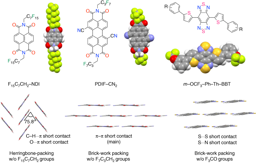
Figure 3.16 (a) Chemical structures, molecular structure (space filling model), and packing structures of F15C7CH2–NDI, PDIF–CN2, and m‐OCF3–Ph–Th–BBT. F15C7CH2, F7C3CH2, and m‐OCF3 groups for each molecule are omitted for clarity, respectively.
Yamashita et al. developed novel n‐type materials based on a benzobis(thiazole) (BBT) units having low LUMO level (−4.04 eV, determined by cyclic voltammetry) showing high mobility (0.77 cm2 V−1 s−1) and good air stability [89]. Very recently, Tokito et al. further addressed the development of soluble n‐type organic semiconductors based on BBT by introducing a novel molecular design of the simple substitution of trifluoromethyl or trifluoromethoxy groups at the meta positions of phenyl terminal units to support sufficient solubility, creating suitable LUMO energy levels and high crystallinity. These newly designed BBT‐based molecules showed electron mobilities as high as 0.61 cm2 V−1 s−1 in solution‐processed OFETs [90].
Summary and Future Outlook for Molecular Technology of Organic Semiconductors
In this chapter, the author has focused on representative p‐ and n‐type organic semiconductors mainly for the application of OFETs. The acene‐ and heteroacene‐based molecules for p‐type semiconductors and the acenes and heteroacenes exhibiting strong electron‐withdrawing groups such as diimide and fluoro groups and so on for n‐type semiconductors are described. Their electronic structures such as the configuration of HOMOs and LUMOs, their energy levels, and electrostatic potential maps can be facilely visualized and understood by theoretical calculations. The packing structures of acenes and heteroacenes form either one‐dimensional π‐stack or two‐dimensional herringbone‐type packing, and the latter case is favorable for charge transport. As discussed several organic semiconducting molecules in the aggregated form, the degree of their orbital overlaps depends on the configuration of HOMO or LUMO as well as their packings. Before the transistor evaluation, the orbital overlaps in the aggregated form could be quantitatively understood by calculating transfer integrals between the neighboring molecules, facilitating the screening of highly potential organic semiconductors in this stage. Such a recent research via molecular technology obtained by understanding the relationship between the aggregated structure and carrier transport is crucial for accelerating development of next‐generation superior organic semiconductors. As one example, very recently, outstanding results on p‐type semiconducting molecules is that conceptually new bent‐shaped π‐cores show a mobility of more than 10 cm2 V−1 s−1 in solution‐crystallized thin‐film FETs along with highly crystalized phase of more than 200 °C. This result is ideal for further practical device‐fabrication processes as well as for next‐generation organic semiconductors. On the other hand, the mobility of n‐type semiconductors is still one order lower than that of p‐type semiconductors, whereas several types of n‐type semiconductors have been recently reported. Therefore, toward high‐electron‐mobility organic semiconductors, conceptually new molecules and aggregated forms based on molecular technology should be emergently proposed and investigated for realizing future printable and flexible electronics applications (Figure 3.17).

Figure 3.17 Hole and electron mobilities vs market size. Representative solution‐processable organic semiconductors along with high performance and high chemical stability.
References
- 1 Bao, Z. and Locklin, J. (2007). Organic Field‐Effect Transistors, 1ste. Florida: CRC Press.
- 2 Müllen, K. and Scherf, U. (2006). Organic Light‐Emitting Devices: Synthesis, Properties and Applications. Wiley‐VCH.
- 3 Sun, S.‐S. and Sariciftci, N.S. (2005). Organic Photovoltaics: Mechanism, Materials, and Devices. CRC Press.
- 4 Anthony, J.E. (2006). Chem. Rev. 106: 5028.
- 5 Coropceanu, V., Cornil, J., da Silva Filho, D.A. et al. (2007). Chem. Rev. 107: 926.
- 6 Takimiya, K., Shinamura, S., Osaka, I., and Miyazaki, E. (2011). Adv. Mater. 23: 4347.
- 7 Kuribara, K., Wang, H., Uchiyama, N. et al. (2012). Nat. Commun. 3: 723.
- 8 Troisi, A., Cheung, D.L., and Andrienko, D. (2009). Phys. Rev. Lett. 102: 116602.
- 9 Uemura, T., Yamagishi, M., Soeda, J. et al. (2012). Phys. Rev. B 85: 035313.
- 10 Shinar, J. (2004). Organic Light‐Emitting Devices: A Survey. Springer.
- 11 Lin, P. and Yan, F. (2012). Adv. Mater. 24: 34.
- 12 Capelli, S.C., Albinati, A., Mason, S.A., and Willis, B.T.M. (2006). J. Phys. Chem. A 110: 11695.
- 13 Lusi, M., Vitorica‐Yrezabal, I.J., and Zaworotko, M.J. (2015). Cryst. Growth Des. 15: 4098.
- 14 Holmes, D., Kumaraswamy, S., Matzger, A.J., and Vollhardt, K.P.C. (1999). Chem. Eur. J. 5: 3399.
- 15 Mattheus, C.C., Dros, A.B., Baas, J. et al. (2001). Acta Crystallogr. C 57: 939.
- 16 Nishio, M., Hirota, M., and Umezawa, Y. (1998). The CH/π Interaction: Evidence, Nature, and Consequences, vol. 1998. New York: Wiley‐VCH.
- 17 Cox, E.G. and Smith, J.A.S. (1954). Nature 173: 75.
- 18 Nayak, S.K., Sathishkumar, R., and Row, T.N.G. (2010). CrystEngComm 12: 3112.
- 19 Tsuzuki, S., Honda, K., Uchimaru, T. et al. (2002). J. Am. Chem. Soc. 124: 104.
- 20 Tsuzuki, S., Honda, K., Uchimaru, T., and Mikami, M. (2004). J. Chem. Phys. 120: 647.
- 21 Warta, W., Stehle, R., and Karl, N. (1985). Appl. Phys. A: Solids Surf. 36: 163.
- 22 Klauk, H., Halik, M., Zschieschang, U. et al. (2002). J. Appl. Phys. 92: 5259.
- 23 Gundlach, D.J., Nichols, J.A., Zhou, L., and Jackson, T.N. (2002). Appl. Phys. Lett. 80: 2925.
- 24 Kloc, C., Simpkins, P.G., Siegrist, T., and Laudise, R.A. (1997). J. Cryst. Growth 182: 416.
- 25 Laudise, R.A., Kloc, C., Simpkins, P.G., and Siegrist, T. (1998). J. Cryst. Growth 187: 449.
- 26 Goldmann, C., Haas, S., Krellner, C. et al. (2004). J. Appl. Phys. 96: 2080.
- 27 Jurchescu, O.D., Baas, J., and Palstra, T.T.M. (2004). Appl. Phys. Lett. 84: 3061.
- 28 Jurchescu, O.D., Popinciuc, M., van Wees, B.J., and Palstra, T.T.M. (2007). Adv. Mater. 19: 688.
- 29 Takeya, J., Yamagishi, M., Tominari, Y. et al. (2007). Appl. Phys. Lett. 90: 102120.
- 30 Maliakal, A., Raghavachari, K., Katz, H. et al. (2004). Chem. Mater. 16: 4980.
- 31 Laquindanum, J.G., Katz, H.E., and Lovinger, A.J. (1998). J. Am. Chem. Soc. 120: 664.
- 32 Tang, M.L., Okamoto, T., and Bao, Z. (2006). J. Am. Chem. Soc. 128: 16002.
- 33 Yamada, K., Okamoto, T., Kudoh, K. et al. (2007). Appl. Phys. Lett. 90: 072102.
- 34 Xiao, K., Liu, Y., Qi, T. et al. (2005). J. Am. Chem. Soc. 127: 13281.
- 35 Vyas, V.S., Gutzler, R., Nuss, J. et al. (2014). CrystEngComm 16: 7389.
- 36 Takimiya, K., Ebata, H., Sakamoto, K. et al. (2006). J. Am. Chem. Soc. 128: 12604.
- 37 Yamamoto, T. and Takimiya, K. (2007). J. Am. Chem. Soc. 129: 2224.
- 38 Niimi, K., Shinamura, S., Osaka, I. et al. (2011). J. Am. Chem. Soc. 133: 8732.
- 39 ADF2008.01;SCM Theoretical Chemistry. Amsterdam, The Netherlands: Vrije Universiteit http://www.scm.com (last accessed 23 December 2017.
- 40 Senthilkumar, K., Grozema, F.C., Bickelhaupt, F.M., and Siebbeles, L.D.A. (2003). J. Chem. Phys. 119: 9809.
- 41 Prins, P., Senthilkumar, K., Grozema, F.C. et al. (2005). J. Phys. Chem. B 109: 18267.
- 42 Gundlach, D.J., Lin, Y.Y., Jackson, T.N. et al. (1997). IEEE Electron Device Lett. 18: 87.
- 43 Lin, Y.Y., Gundlach, D.J., Nelson, S.F., and Jackson, T.N. (1997). IEEE Electron Device Lett. 18: 606.
- 44 Klauk, H., Halik, M., Zschieschang, U. et al. (2003). Appl. Phys. Lett. 82: 4175.
- 45 Kelley, T.W., Boardman, L.D., Dunbar, T.D. et al. (2003). J. Phys. Chem. B 107: 5877.
- 46 Masatoshi, K. and Yasuhiko, A. (2008). J. Phys. Condens. Matter 20: 184011.
- 47 Anthony, J.E., Brooks, J.S., Eaton, D.L., and Parkin, S.R. (2001). J. Am. Chem. Soc. 123: 9482.
- 48 Payne, M.M., Parkin, S.R., Anthony, J.E. et al. (2005). J. Am. Chem. Soc. 127: 4986.
- 49 Dickey, K.C., Anthony, J.E., and Loo, Y.L. (2006). Adv. Mater. 18: 1721.
- 50 Park, S.K., Jackson, T.N., Anthony, J.E., and Mourey, D.A. (2007). Appl. Phys. Lett. 91: 063514.
- 51 Diao, Y., Tee, B.C.K., Giri, G. et al. (2013). Nat. Mater. 12: 665.
- 52 Giri, G., Park, S., Vosgueritchian, M. et al. (2014). Adv. Mater. 26: 487.
- 53 Lee, J., Bruzek, M.J., Thompson, N.J. et al. (2013). Adv. Mater. 25: 1445.
- 54 Purushothaman, B., Parkin, S.R., and Anthony, J.E. (2010). Org. Lett. 12: 2060.
- 55 Ebata, H., Izawa, T., Miyazaki, E. et al. (2007). J. Am. Chem. Soc. 129: 15732.
- 56 Uemura, T., Hirose, Y., Uno, M. et al. (2009). Appl. Phys. Express 2: 111501.
- 57 Yuan, Y., Giri, G., Ayzner, A.L. et al. (2014). Nat. Commun. 5: 3005.
- 58 Minemawari, H., Yamada, T., Matsui, H. et al. (2011). Nature 475: 364.
- 59 Kang, M.J., Doi, I., Mori, H. et al. (2011). Adv. Mater. 23: 1222.
- 60 Nakayama, K., Hirose, Y., Soeda, J. et al. (2011). Adv. Mater. 23: 1626.
- 61 Iino, H., Usui, T., and Hanna, J.‐i. (2015). Nat. Commun. 6: 6828.
- 62 Minari, T., Kano, M., Miyadera, T. et al. (2008). Appl. Phys. Lett. 92: 173301.
- 63 Kano, M., Minari, T., and Tsukagoshi, K. (2010). Appl. Phys. Express 3: 051601.
- 64 Giri, G., Verploegen, E., Mannsfeld, S.C.B. et al. (2011). Nature 480: 504.
- 65 Liu, C., Minari, T., Lu, X. et al. (2011). Adv. Mater. 23: 523.
- 66 Kuwabara, H., Ikeda, M., and Takimiya, K. (2010). Field effect transistors provided with condensed heterocyclic aromatic compounds, WO 2010/098372 A1.
- 67 Chen, J., Anthony, J., and Martin, D.C. (2006). J. Phys. Chem. B 110: 16397.
- 68 Sundar, V.C., Zaumseil, J., Podzorov, V. et al. (2004). Science 303: 1644.
- 69 Reese, C., Chung, W.‐J., Ling, M.‐m. et al. (2006). Appl. Phys. Lett. 89: 202108.
- 70 Mitsui, C., Soeda, J., Miwa, K. et al. (2012). J. Am. Chem. Soc. 134: 5448.
- 71 Niimi, K., Mori, H., Miyazaki, E. et al. (2012). Chem. Commun. 48: 5892.
- 72 Tsuji, H., Shoyama, K., and Nakamura, E. (2012). Chem. Lett. 41: 957.
- 73 Watanabe, M., Su, W.‐T., Chang, Y.J. et al. (2013). Chem. Asian J. 8: 60.
- 74 Gidron, O., Dadvand, A., Sheynin, Y. et al. (2011). Chem. Commun. 47: 1976.
- 75 Nakahara, K., Mitsui, C., Okamoto, T. et al. (2014). Chem. Commun. 50: 5342.
- 76 Mitsui, C., Kubo, W., Tanaka, Y. et al. (2017). Chem. Lett. 46: 338.
- 77 Mitsui, C., Tanaka, Y., Tanaka, S. et al. (2016). RSC Adv. 6: 28966.
- 78 Naraso, H., Nishida, J.‐I., Kumaki, D. et al. (2006). J. Am. Chem. Soc. 128: 9598.
- 79 Newman, C.R., Frisbie, C.D., da Silva Filho, D.A. et al. (2004). Chem. Mater. 16: 4436.
- 80 de Leeuw, D.M., Simenon, M.M.J., Brown, A.R., and Einerhand, R.E.F. (1997). Synth. Met. 87: 53.
- 81 Katz, H.E., Lovinger, A.J., Johnson, J. et al. (2000). Nature 404: 478.
- 82 Bao, Z., Lovinger, A.J., and Brown, J. (1998). J. Am. Chem. Soc. 120: 207.
- 83 Jones, B.A., Facchetti, A., Wasielewski, M.R., and Marks, T.J. (2007). J. Am. Chem. Soc. 129: 15259.
- 84 He, T., Stolte, M., Burschka, C. et al. (2015). Nat. Commun. 6: 5954.
- 85 Horowitz, G., Kouki, F., Spearman, P. et al. (1996). Adv. Mater. 8: 242.
- 86 Chesterfield, R.J., McKeen, J.C., Newman, C.R. et al. (2004). J. Phys. Chem. B 108: 19281.
- 87 Jones, B.A., Ahrens, M.J., Yoon, M.‐H. et al. (2004). Angew. Chem. Int. Ed. 43: 6363.
- 88 Molinari, A.S., Alves, H., Chen, Z. et al. (2009). J. Am. Chem. Soc. 131: 2462.
- 89 Kono, T., Kumaki, D., Nishida, J.‐I. et al. (2010). Chem. Commun. 46: 3265.
- 90 Mamada, M., Shima, H., Yoneda, Y. et al. (2015). Chem. Mater. 27: 141.