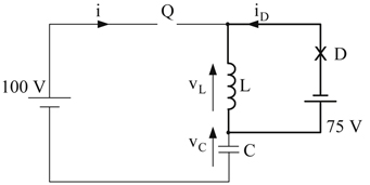
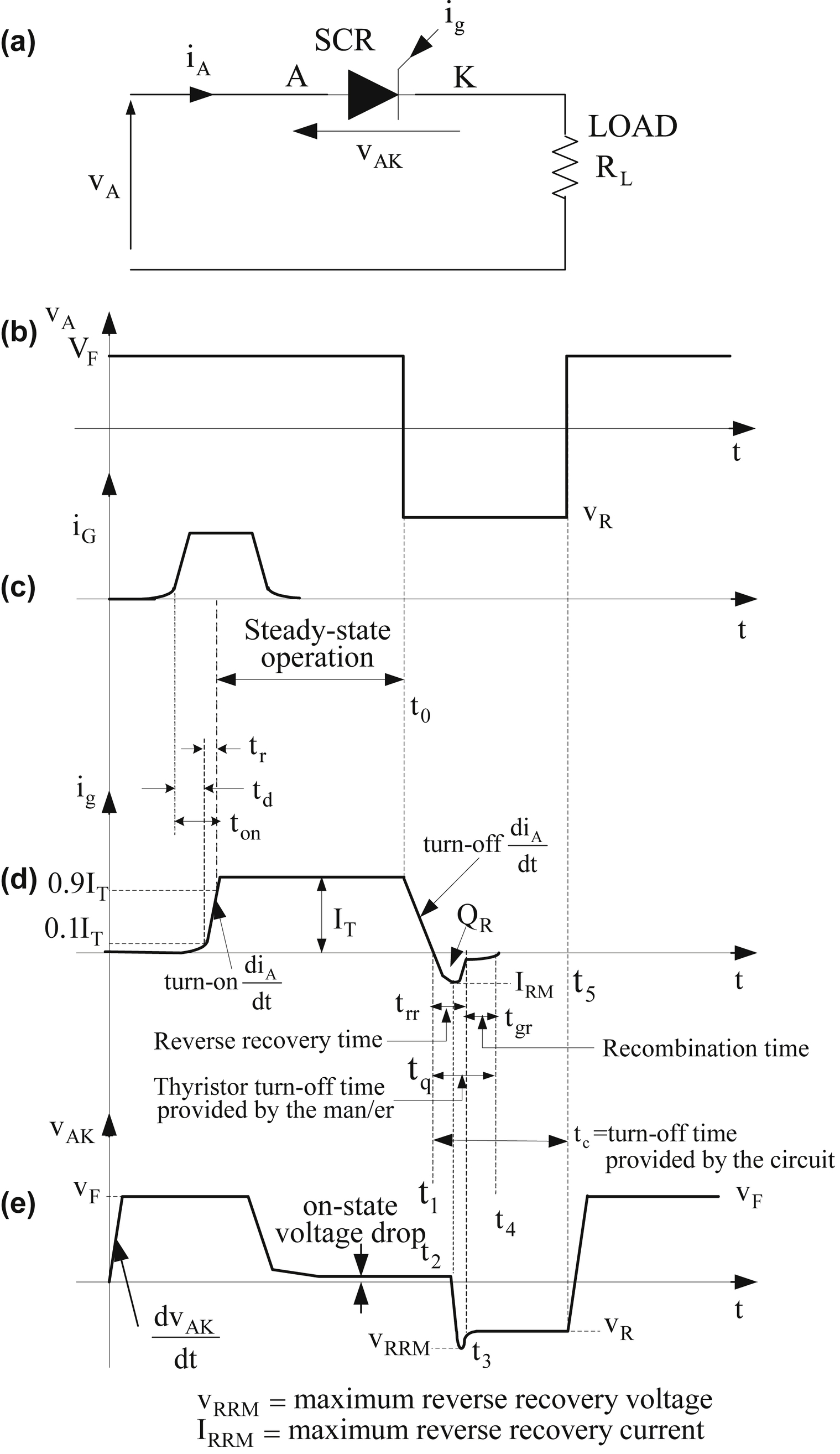
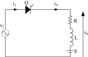
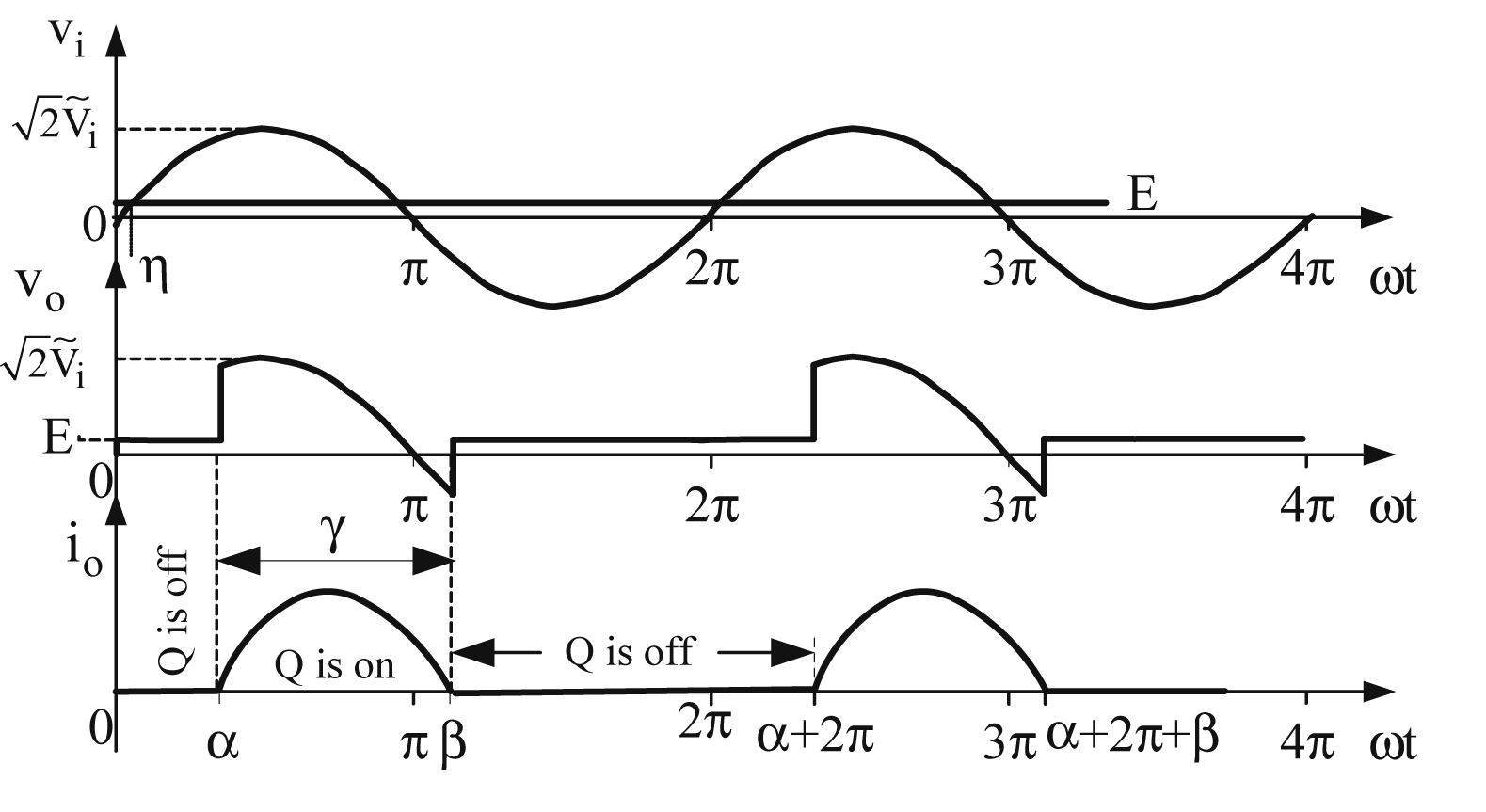
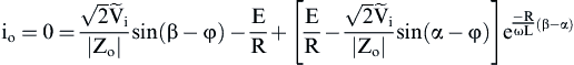
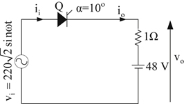
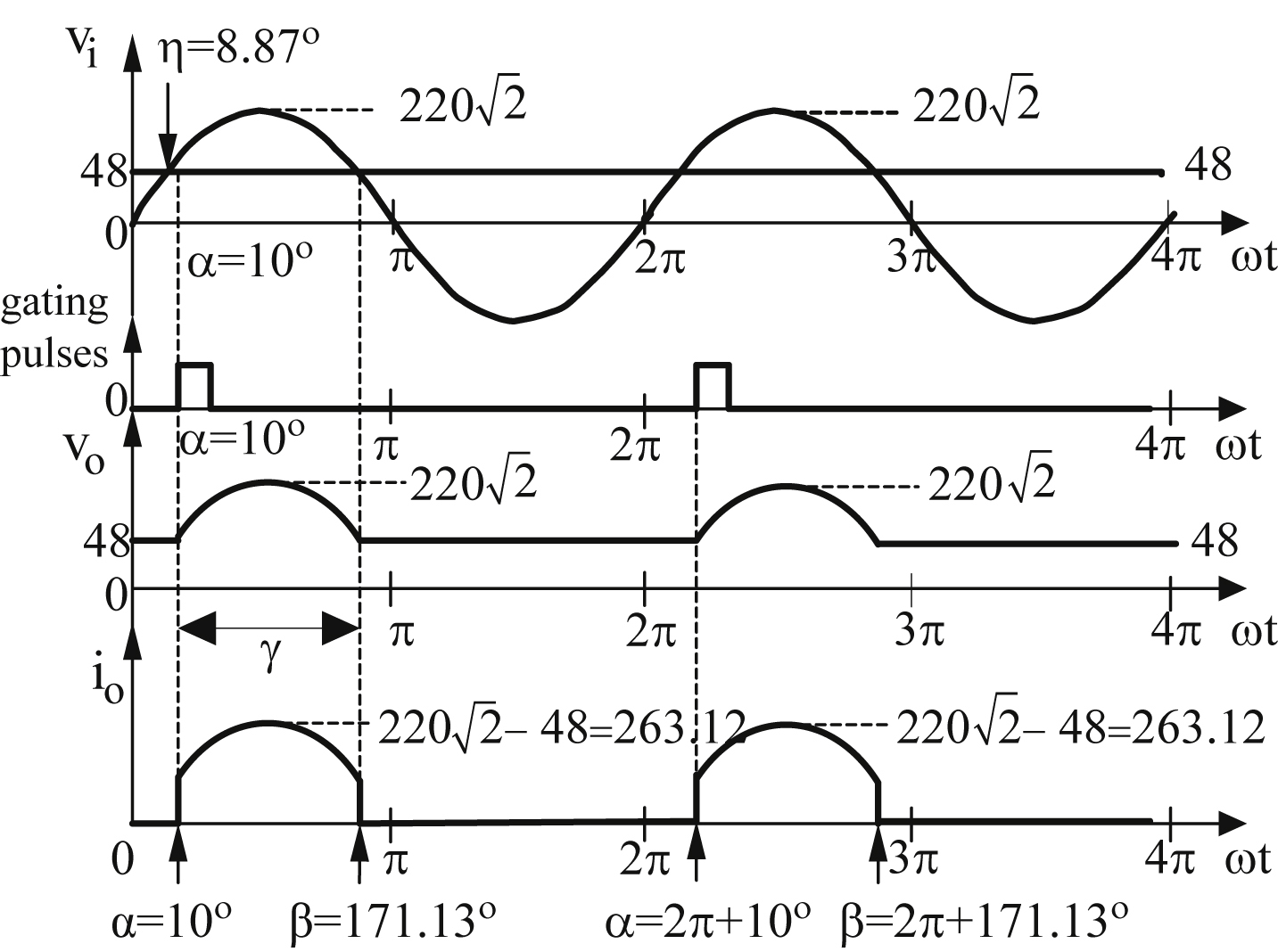
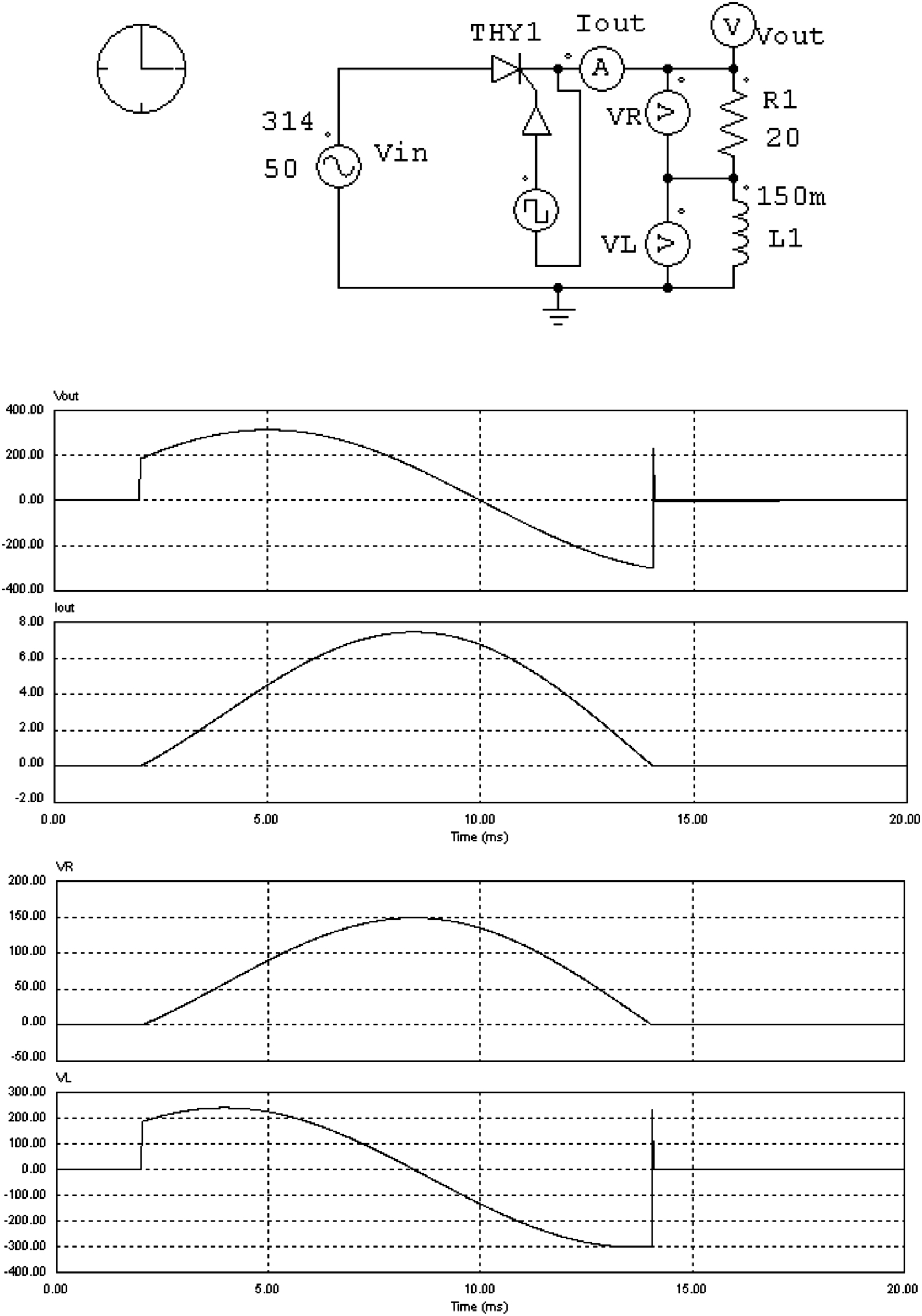
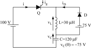
Fig. 3.6(a) shows a thyristor circuit which will be used to study the switching characteristics of a thyristor. Moreover,
Fig. 3.6(b)–(e) present the different waveforms which will be used to explain the dynamic behavior of a thyristor. As
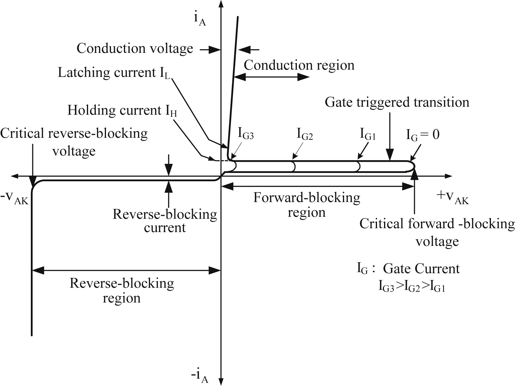
Fig. 3.6(a) indicates, initially the input voltage v
A is positive and, consequently, the thyristor is in the forward-blocking state. If a gating pulse is applied during this state, there is a delay time t
d before the anode current i
A starts rising. This delay time, shown in
Fig. 3.6(d), is approximately some microseconds and it is due to the charge movement inside the thyristor device. At the end of time t
d the current starts flowing through the thyristor. When the thyristor is in the on state the current starts increasing until it reaches its final value I
T, with a rate of rise di/dt (
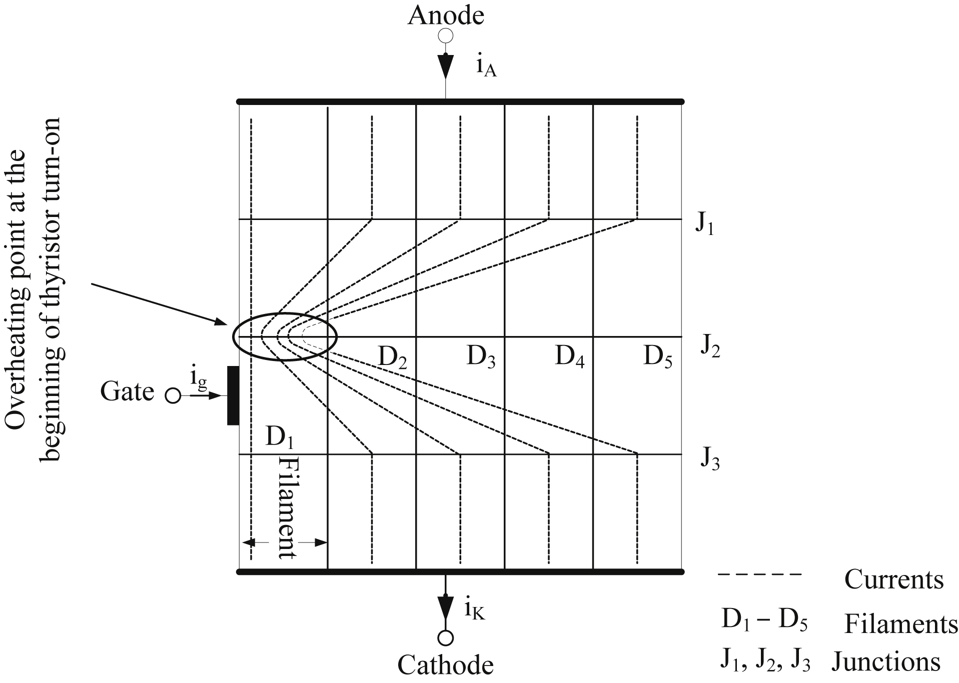
Fig. 3.6(d)). The maximum value of di/dt is given by the manufacturer and has to be respected by the designer because beyond this value the thyristor will be destroyed due to local overheating (hot spot). This hot spot is due to the fact that during the thyristor turn on the anode current i
A does not have the appropriate time to be uniformly distributed within the thyristor filaments and there is one section of a filament through which the excessive current flows. This phenomenon is shown in
Fig. 3.7. To avoid thyristor hot spot phenomenon, an inductor of few μH could be connected in series to the thyristor. The same care should be taken with the rate of rise of the
voltage dv
AK/dt (see
Fig. 3.6(e)) when the thyristor goes from the on state to the off state. If the dv
AK/dt exceeds the manufacturer's specifications, then the thyristor will turn on randomly without a gating pulse. The time required for current i
Α to increase from 10% to 90% of its nominal value is called rise time (see
Fig. 3.6(d), t
R). The sum of time intervals t
d and t
r is the turn on time (t
on) of the thyristor (see
Fig. 3.6(d)).
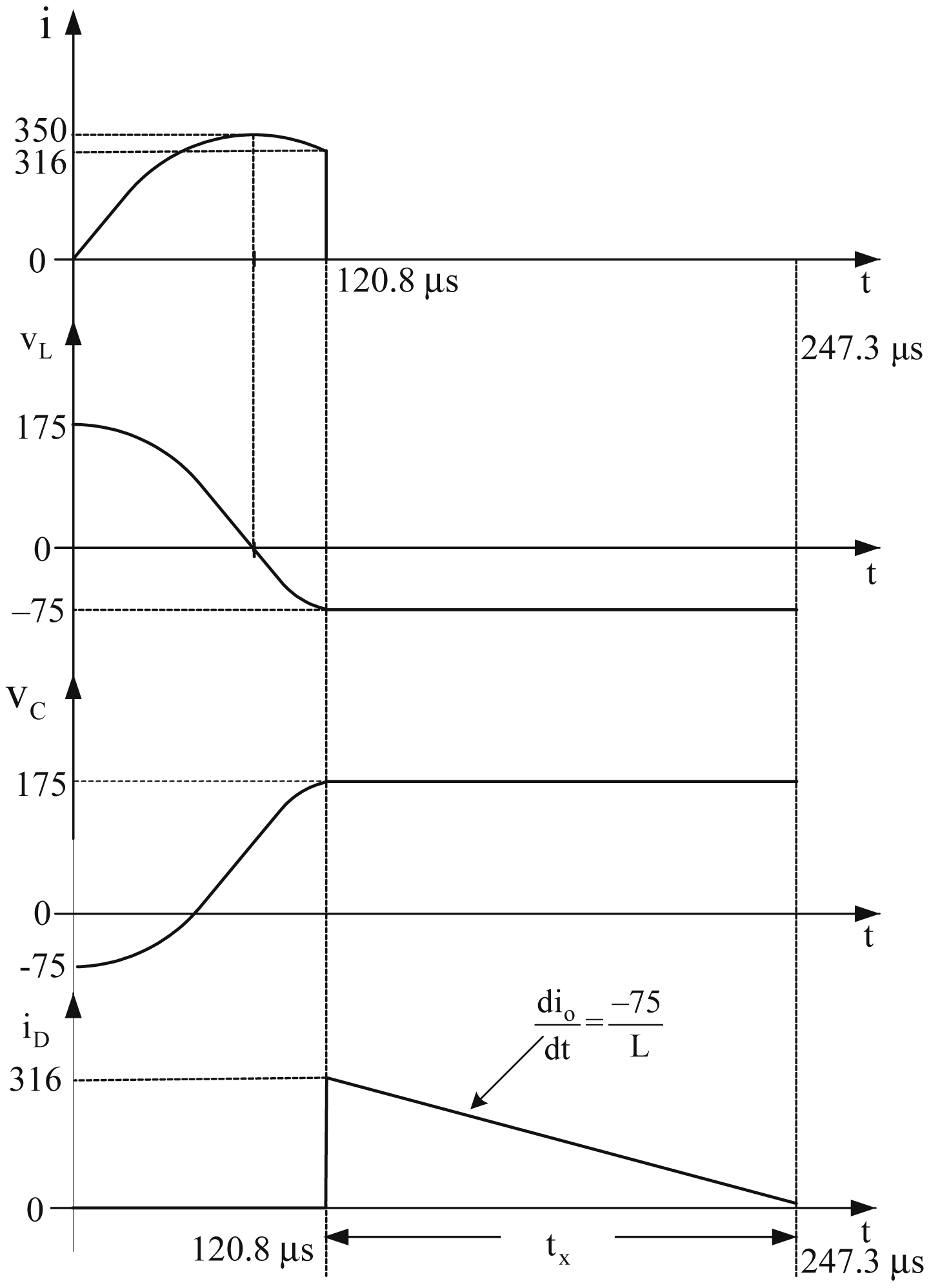
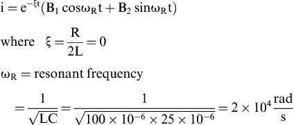
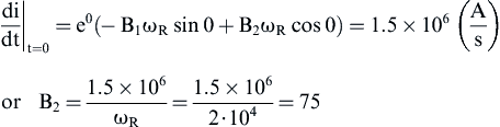
The thyristor turn off starts at the instant t
0 where negative voltage is applied across the anode and cathode terminals (
Fig. 3.6(b) and (e)). During thyristor turn off, a switching time delay from the on state to the off state occurs. As
Fig. 3.6(b) indicates, the anode current from the instant t
0 decreases with a rate of rise di/dt and at the instant t
1 becomes zero. After time instant t
l, anode current becomes negative with the same di/dt slope as before. The reason for the reversal of anode current is due to the presence of carriers stored in the four layers. The reverse recovery current removes excess carriers from the end junctions J
1 and J
3 between the instants t
l and t
3. At instant t
2, when about
60% of the stored charges are removed from the two outer layers, carrier density across J
1 and J
3 begins to decrease and with this reverse recovery current also starts decaying. The reverse current decay is fast in the beginning but gradual thereafter. When the process has ended, the junctions J
1 and J
3 return to blocking state and the anode current at the instant t
3 is approximately zero. The thyristor is now able to block negative voltages, because the junctions J
1 and J
3 are reverse biased. However, junction J
2 remains forward biased due to its trapped charges. The trapped charges around J
2, cannot flow to the external circuit, therefore, these trapped charges must decay only by recombination.
This recombination is possible if a reverse voltage is maintained across thyristor, though the magnitude of this voltage is not important. The phenomenon related to the negative current flow in the thyristor is called reverse recovery and the time reverse recovery time t
rr. The time for the recombination of charges between t
3 and t
4 is called gate recovery time t
gr. As
Fig. 3.6(e) indicates, t
q =
t
rr +
t
gr is the time required by the thyristor to obtain again its forward-blocking capability. It is worth noticing that, if the thyristor voltage V
AK takes positive values before obtaining the forward-blocking capability (i.e., before the end of the time determined by the manufacturer t
q), then the thyristor will be triggered into conduction state without the need of a switch-on pulse to its gate. The turn-off time provided to the thyristor by the power circuit is called circuit turn-off time t
c. It is defined as the time between the instant time the thyristor current becomes zero and the instant time of the reverse voltage due to power circuit reaches zero (see
Fig. 3.6(d)). Time t
c must be greater than t
q for reliable turn off, otherwise the device may turn on at an undesired instant, a process called commutation failure.
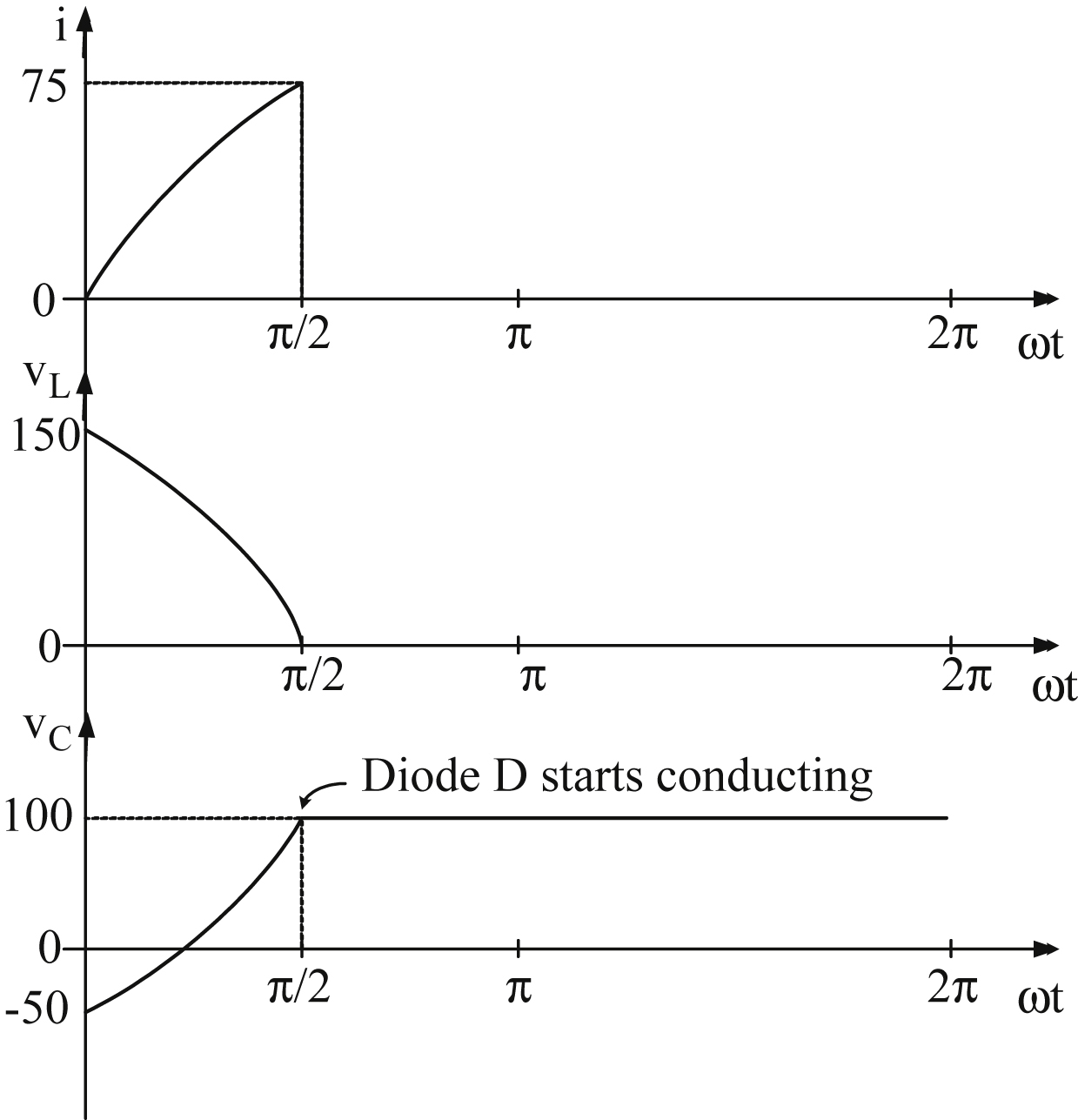
The turn-off process of a thyristor is called commutation. The commutation of a thyristor can be achieved using the following techniques:
The turn-off stages are shown in
Fig. 3.8.
The creation of the thyristor commutation voltages and currents are achieved by applying auxiliary circuits, called commutation circuits. The commutation circuits are part of any power converter, which is implemented with thyristors, and the only way to turn them off is by using force commutation techniques.

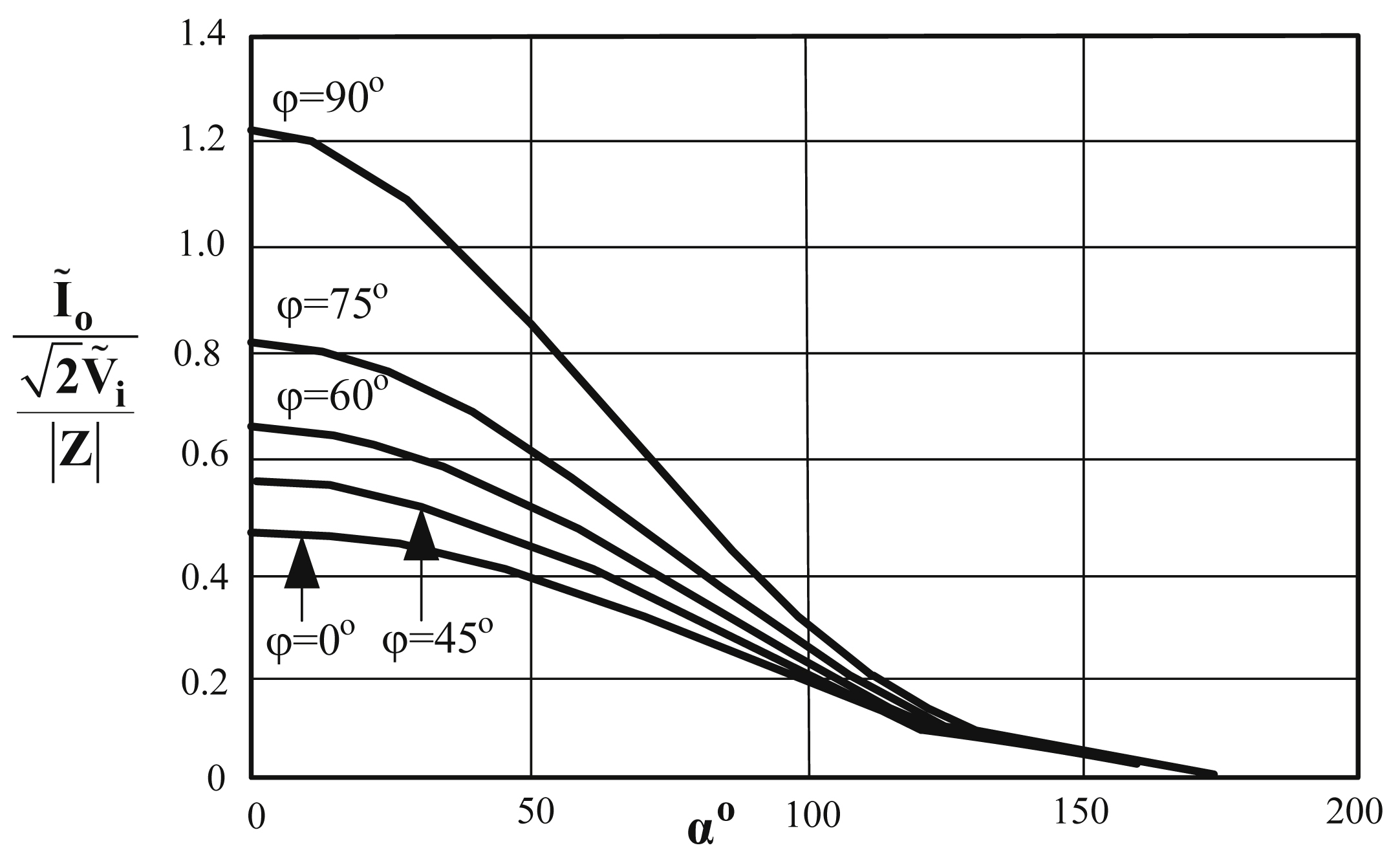
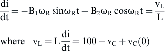
 (3.3)
(3.3)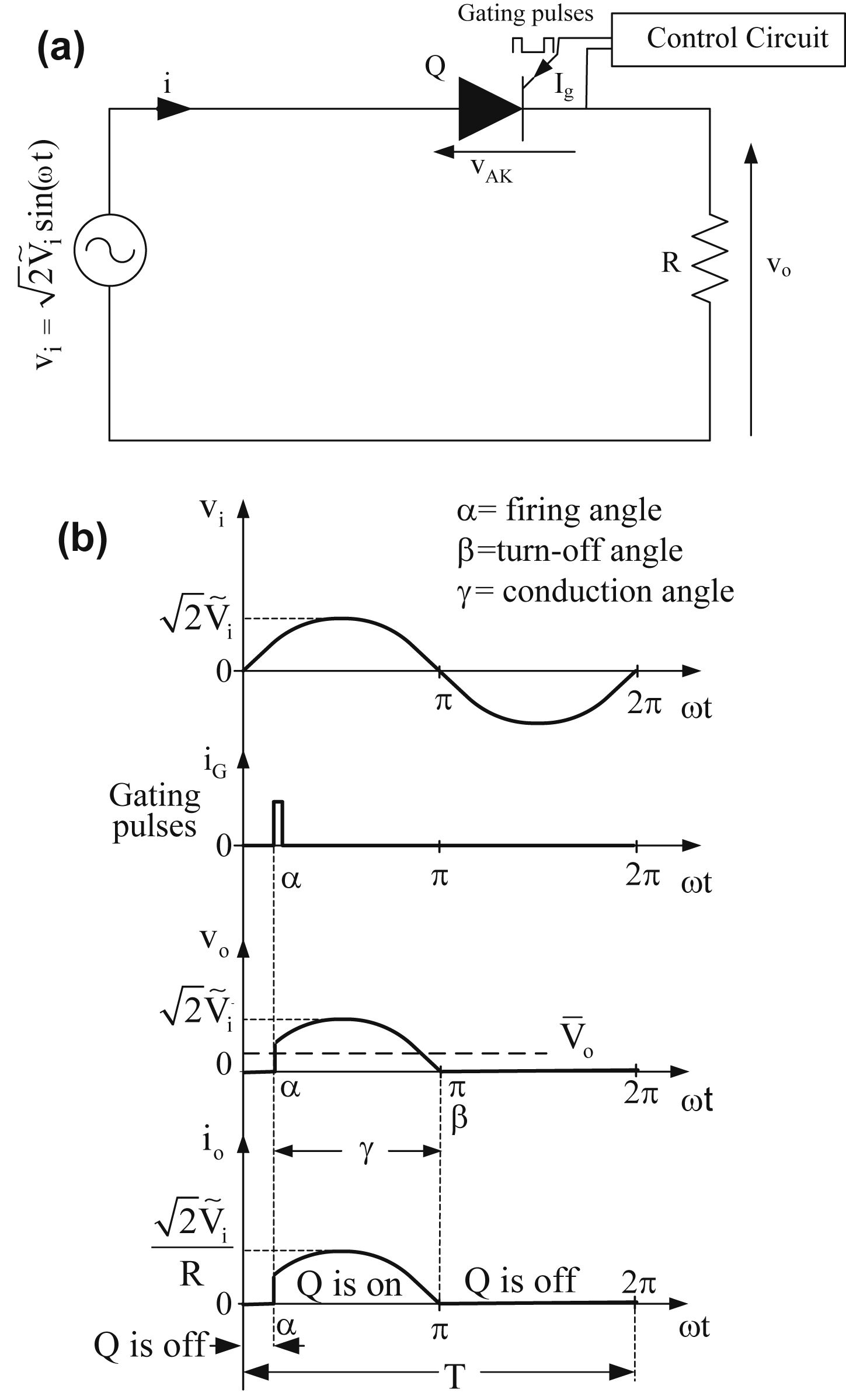
 (3.5)
(3.5)
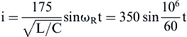
 (3.6)
(3.6)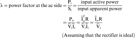 (3.8)
(3.8)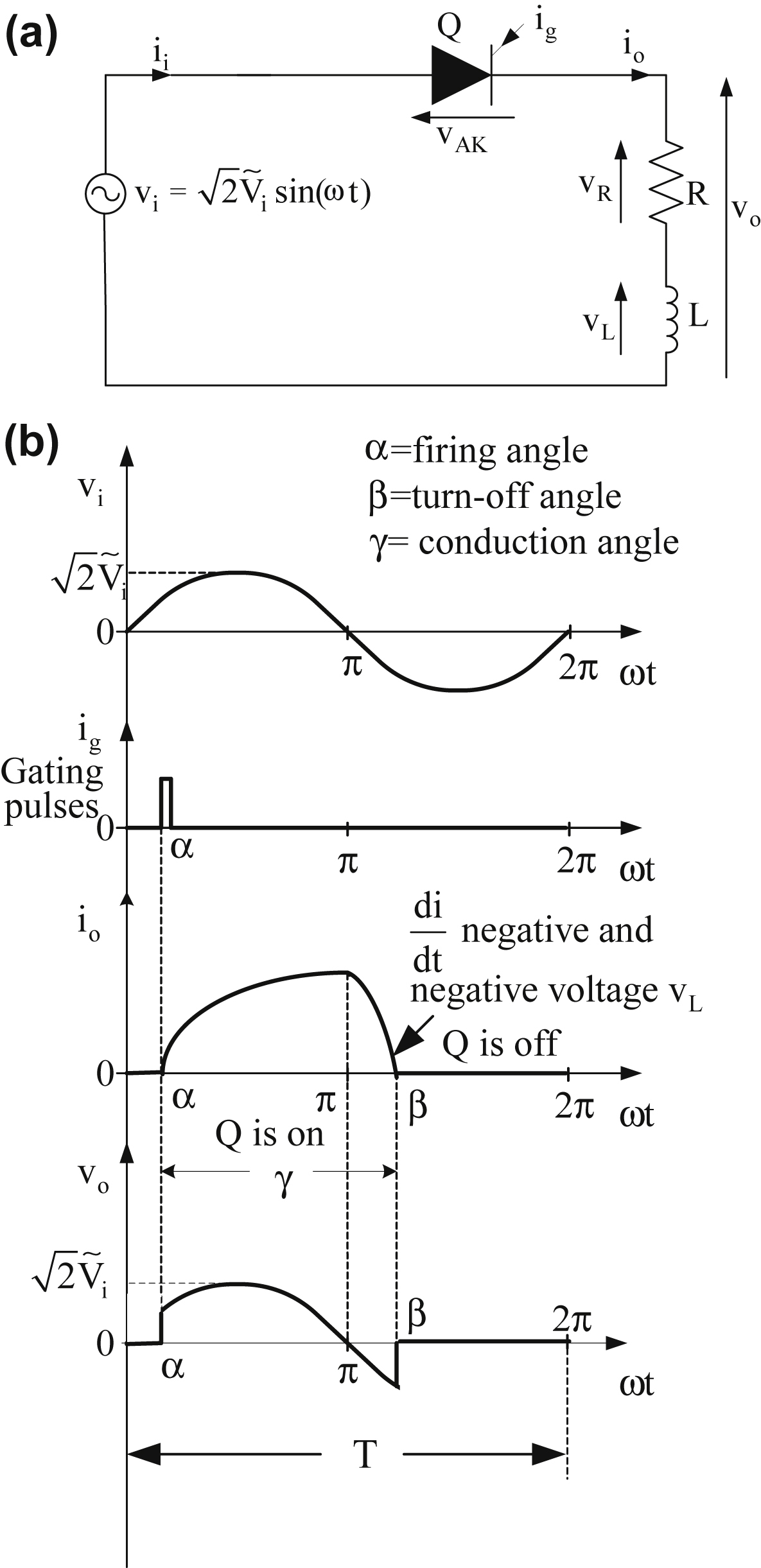
 (3.11)
 (3.12)
 (3.13)
 (3.16)
 (3.17)
 (3.18)


 (3.20)
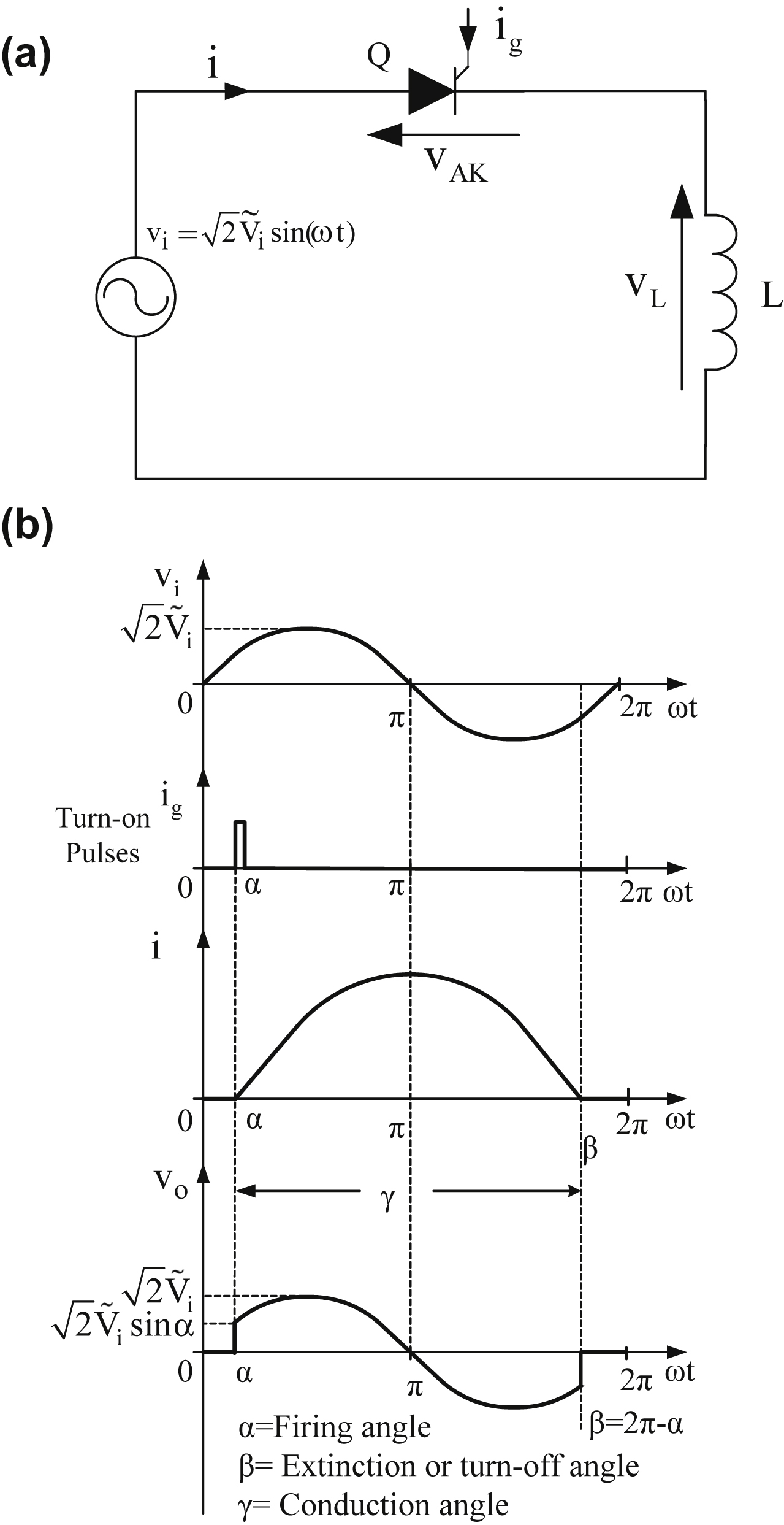
 (3.23)
 (3.24)
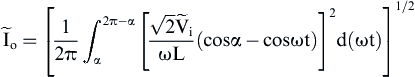 (3.25)
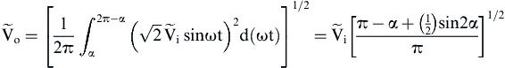 (3.26)
 (3.27)
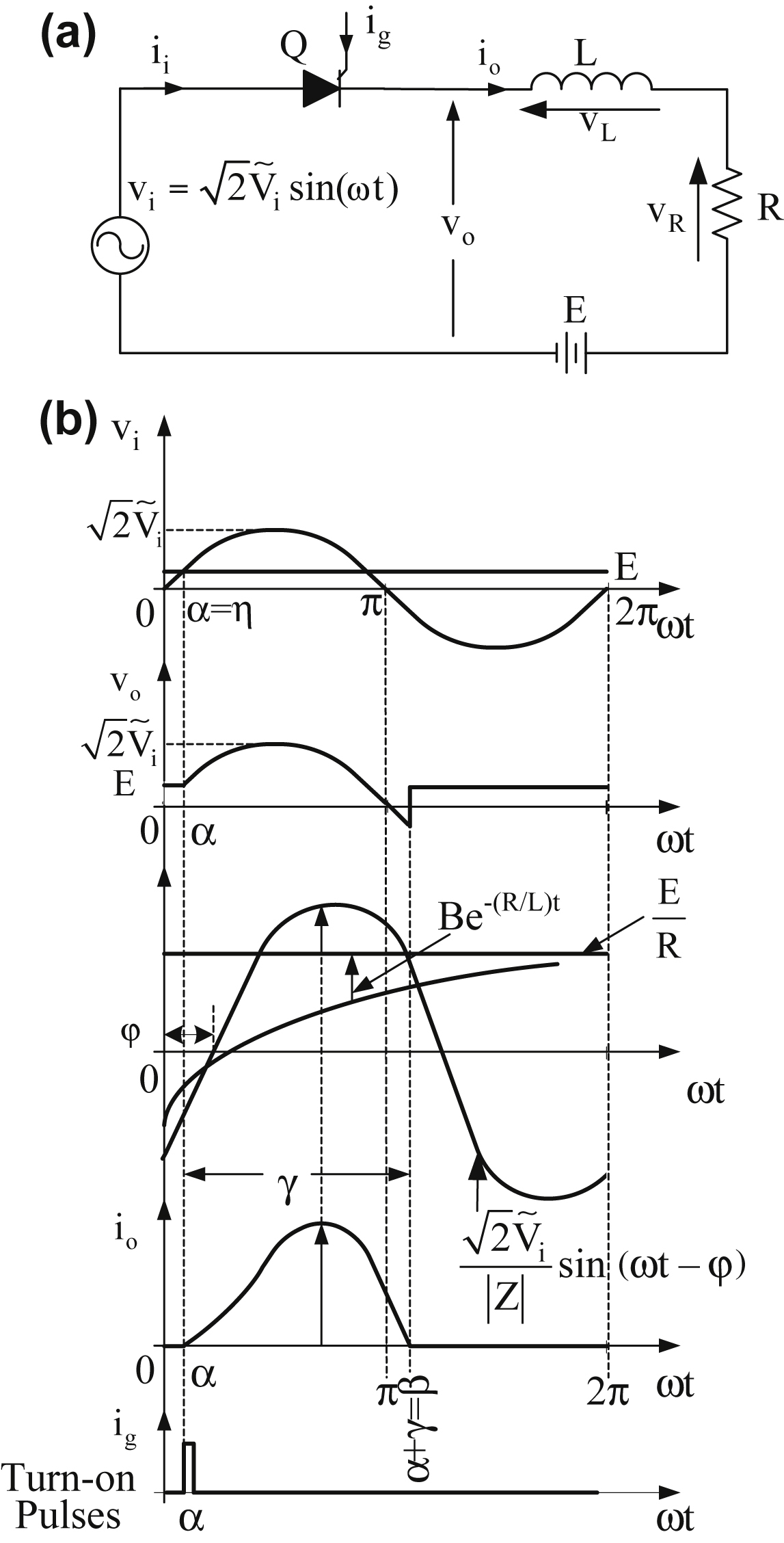
 (3.31)
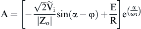
 (3.32)
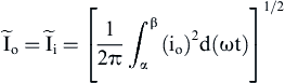 (3.36)
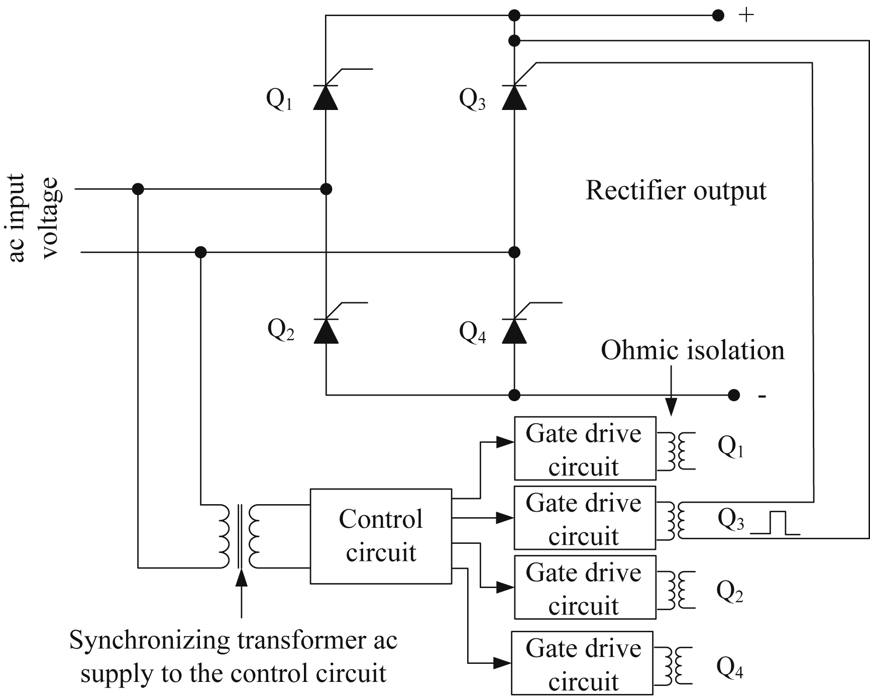
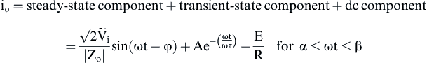
 (1)
(1)

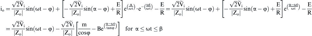
 (3)
(3) (4)
(4) (5)
(5) (7)
(7) (8)
(8) (9)
(9)

 (1)
(1) (3)
(3) (4)
(4) (5)
(5)

 (3)
(3)
 (1)
(1)
 (4)
(4) (5)
(5)
 (6)
(6)