
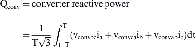
6.9. P–Q Control of a Three-Phase Voltage Source Inverter
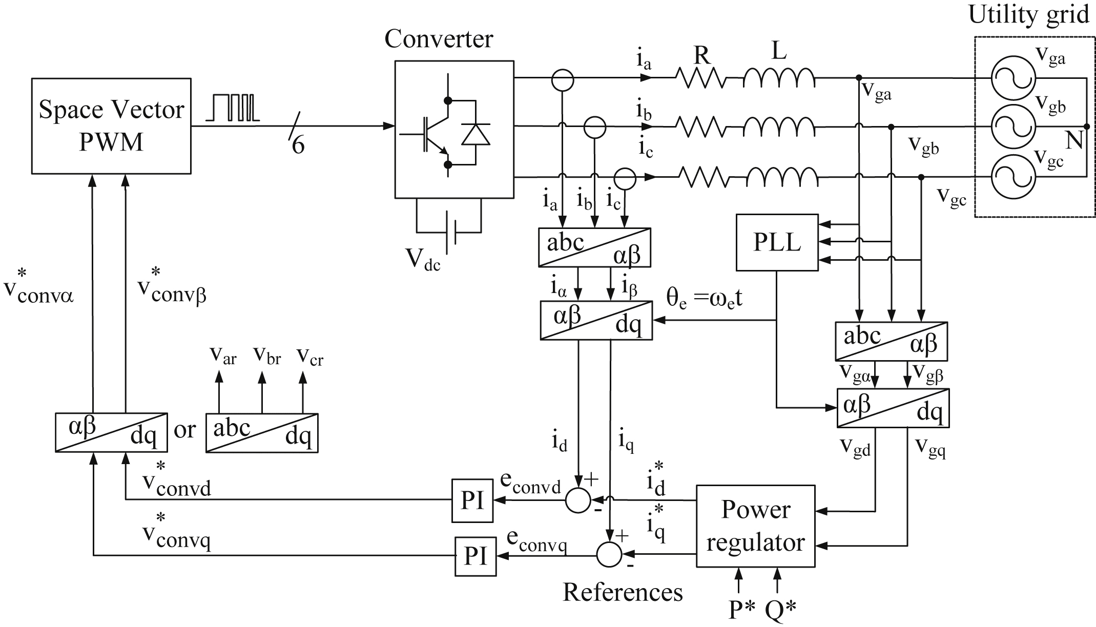
Today a power electronics inverter is used efficiently to control the flow of the active and reactive power between a dc power source and the utility grid acting as a power STATCOM which also finds applications in the interfacing of RES. Fig. 6.135 presents the block diagram of a three-phase VSI, connected to a utility grid (PCC), where  is the fundamental component of the inverter output phase voltage that operates at a voltage amplitude of
  and with a phase displacement δ with respect to the utility grid phase voltage
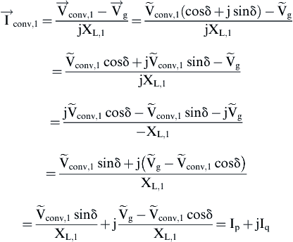
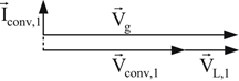
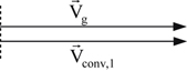
  . The basic and minimum requirement of the VSI is to control the flow of the active and reactive power between the renewable source (i.e., the inverter) and the utility grid. The choice of the control technique of an inverter, which is connected to a utility grid, depends on the utility connection specifications, which include power quality and the control of the power flow from and to the utility grid (P–Q control). As mentioned before in this chapter, the inverter has the ability to operate bidirectionally, thus when is feeding power from its dc input to the utility grid operates as an inverter and when is absorbing power from the utility grid operates as a rectifier. For this reason the inverter in this section will be called converter. Since the voltage of the utility grid is not defined by the converter and can be assumed to be constant, the value and the quality of power delivered or received from the utility grid depend on the generated current at the output of the converter. Assuming that is synchronized with , the phase difference between and to be δ° and ωL >> R, the equivalent single-phase of Fig. 6.135 can be represented by the equivalent circuit of Fig. 6.136(a).
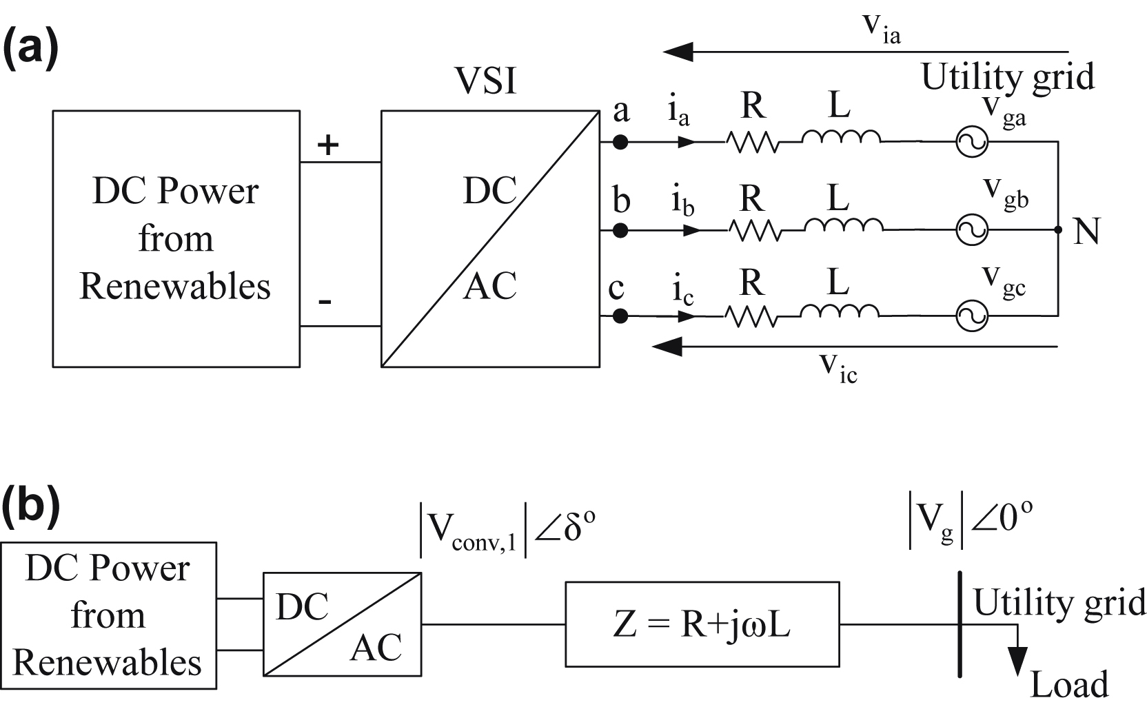
Figure 6.135 Block diagram of a three-phase voltage source converter connected to a point of common coupling of the utility grid.
(a) Three-phase block diagram; (b) single-phase block diagram.
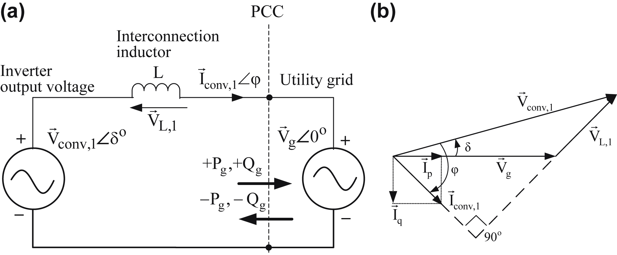

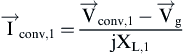
Using Fig. 6.136(a), the following results are obtained:
![]() (6.212)
(6.212)
 (6.213)
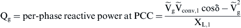
Also, assuming that the output voltage of the converter is pure sinusoidal and knowing, that the conjugate of a + jb = a − jb, then the per-phase apparent power provided by the utility at the PCC (i.e., utility side) is given by:
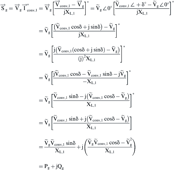 (6.214)
 (6.215)
 (6.216)
 (6.217)
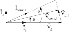
vL,1 = inductor voltage fundamental component
XL,1 = reactance of the interconnection inductor at fundamental frequency
δ = phase difference between utility grid and converter phase voltages
φ = phase displacement between the utility voltage and inverter output current
 (6.218)
 (6.219)
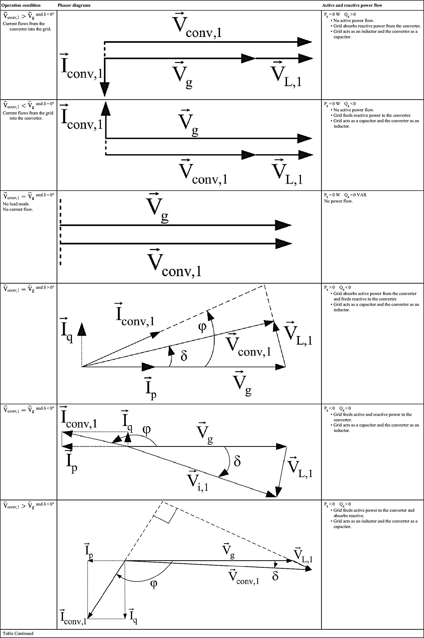
Eqs. (6.218) and (6.219) indicate that the active and reactive power at PCC depend on the converter output voltage  and the phase difference δ. According to Eq. (6.128), the active power at PCC can be controlled by varying the converter output voltage (through the amplitude modulation factor, ma) and the phase angle δ (through the phase displacement between the reference signal vr of the converter and the utility grid). Moreover, according to Eq. (6.127) at the same time, the reactive power at PCC can be controlled only by varying the inverter output voltage . Treating the utility grid as a load to the converter when δ > 0 (i.e., is leading to ), then at PCC Pg > 0, which means that the utility is absorbing active power from the converter. When δ < 0 (i.e., is lagging to ), then Pg < 0, which means that the utility is feeding active power to the converter. When
  , then Qg > 0, which means that the utility is absorbing reactive power from the converter. When
  , then Qg < 0, which means that the utility is feeding reactive power to the converter. Table 6.21 summarizes the power exchange operation modes between the converter and the utility grid with reference the PCC.
Fig. 6.137 presents the Pg and Qg variation with respect to δ and keeping 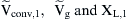 constant. As can be seen in Fig. 6.137 there is a critical value of angle δcritical = 90° at which maximum active power is achieved. If δ is increased beyond this point the system becomes unstable. To avoid such a problem the interconnected supplies must operate at small phase angles (δ ≤ 20°).
Fig. 6.138 presents the Pg–Qg plane operation modes of the inverter-utility transmission system. The range of the phase angle φ is found from the above given figures and equations.
Following the same steps as before the active and reactive power provided by the inverter to the utility can be found as follows:
 (6.220)
Fig. 6.139 presents the block diagram of a STATCOM.
In Chapter 11 the application of the VSI as an active filter will be examined.
Table 6.21
Power exchange modes between utility grid and converter
![]()
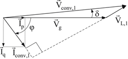
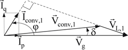
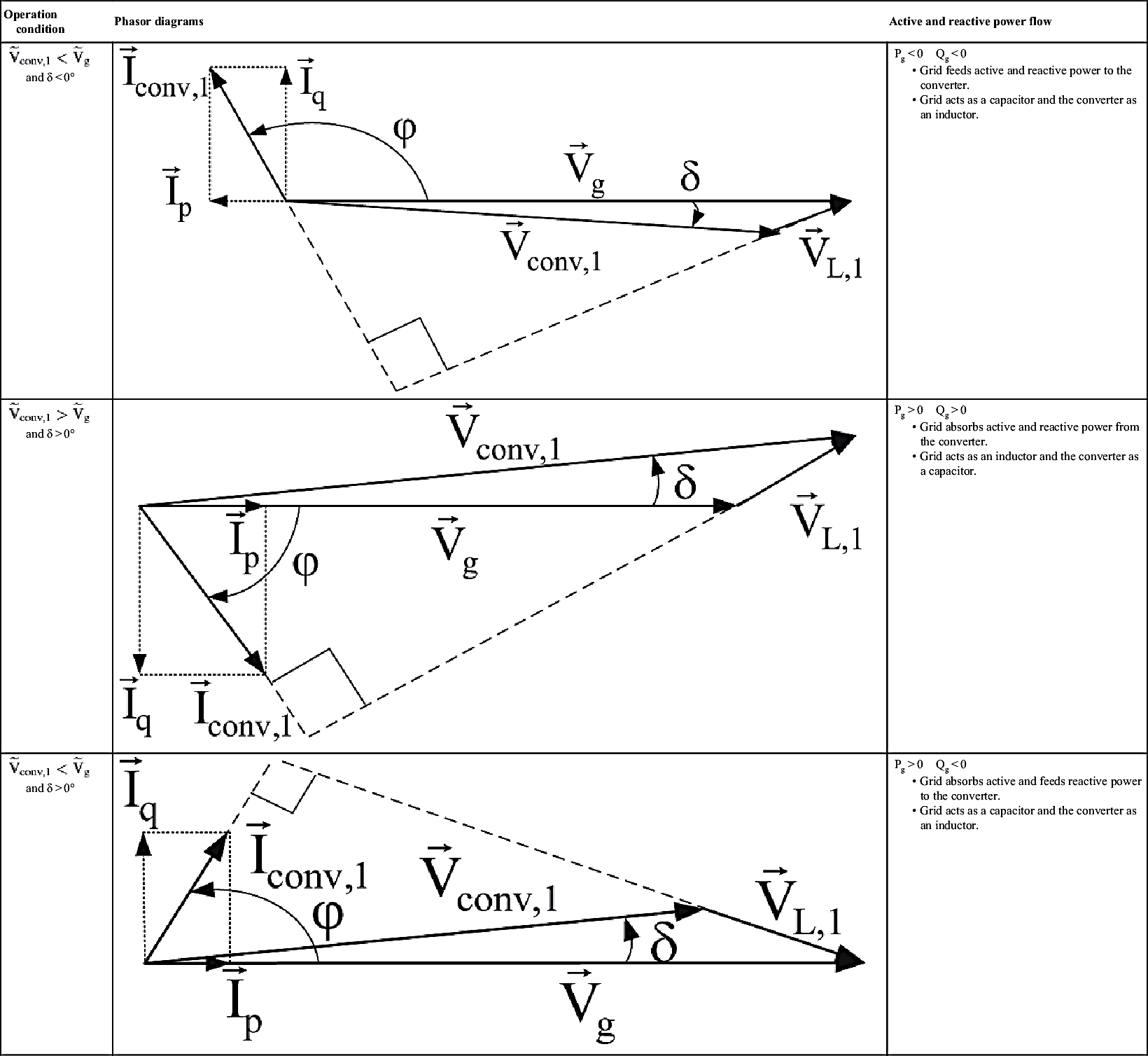
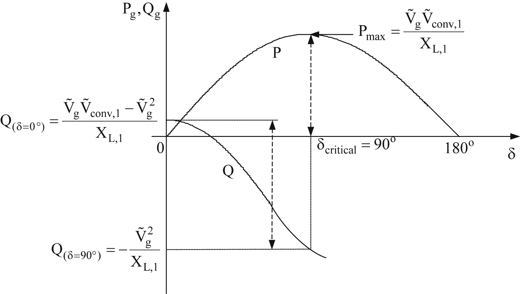

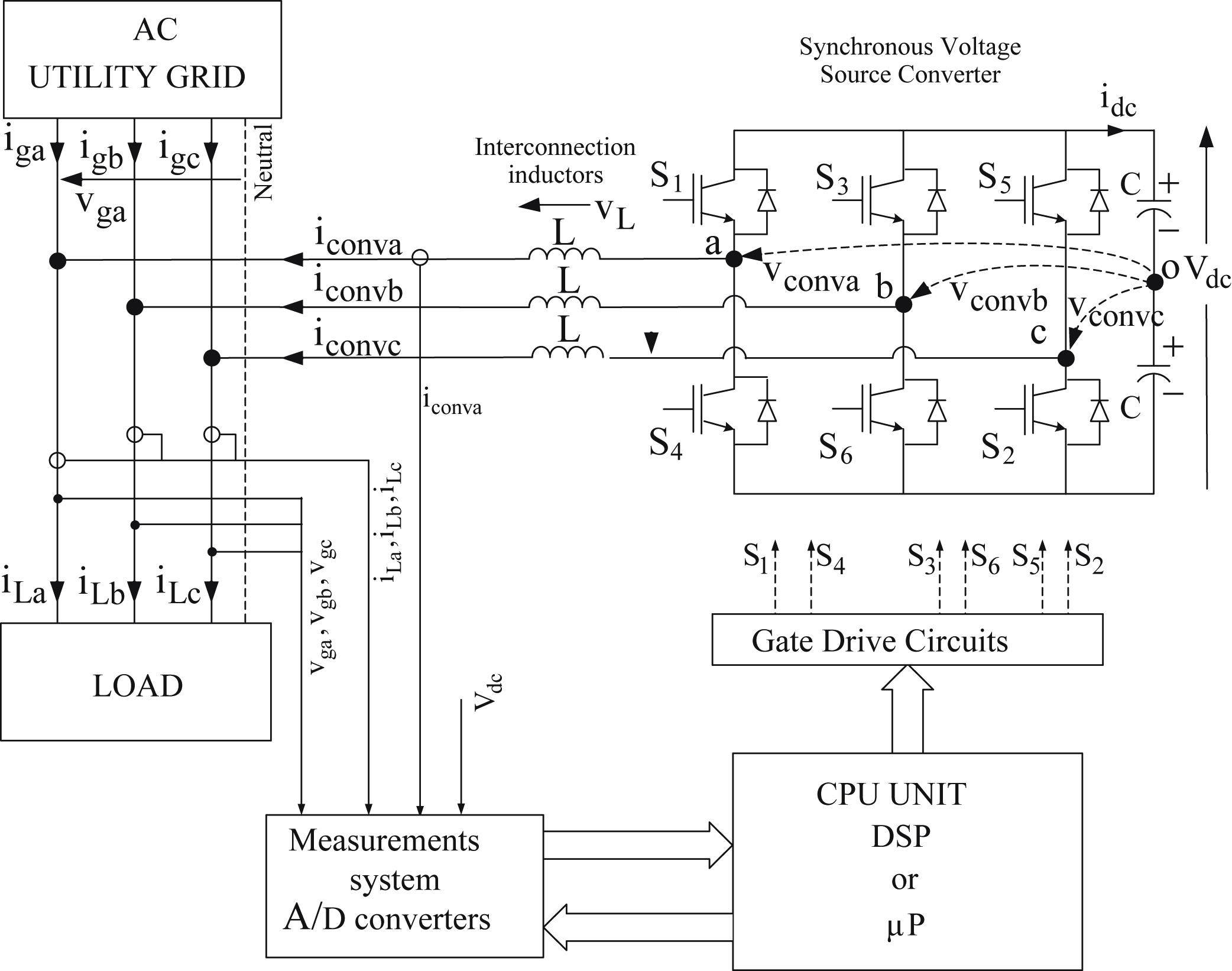
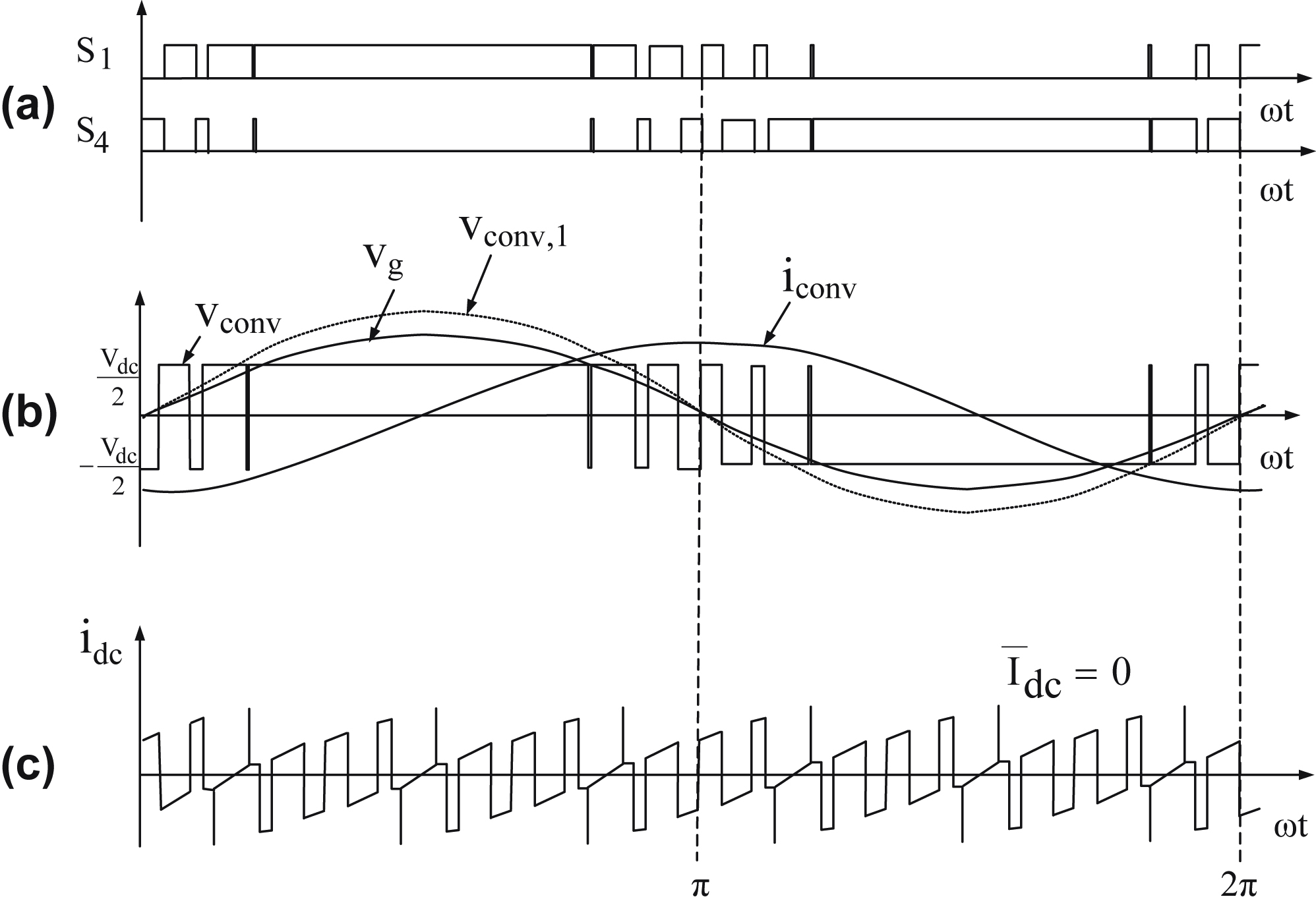
Figure 6.140 Static compensator waveforms when δ = 0°,  , and
, and  . (The utility acts as an inductor absorbing reactive power from the converter.)
(a) Switches S1 and S4 gating signals; (b) utility phase voltage, inverter output phase voltage, and current; (c) dc capacitor current.
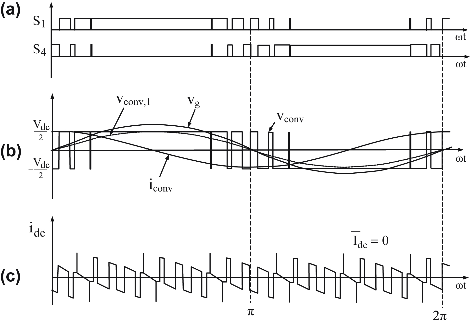
Figure 6.141 Static compensator waveforms when δ = 0°,  , and . (The utility acts as a capacitor feeding reactive power to the converter.)
(a) Switches S1 and S4 gating signals; (b) utility phase voltage, inverter output phase voltage, and current; (c) converter dc capacitor current.
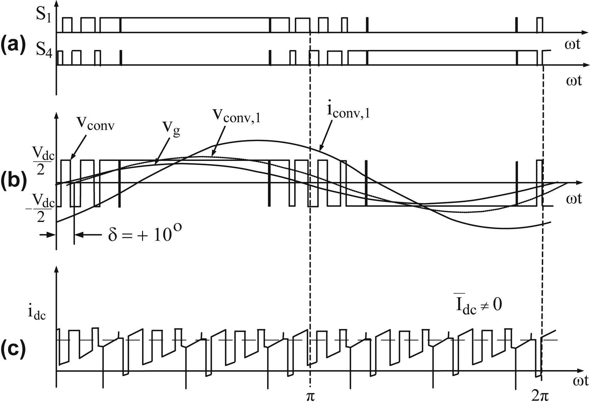
Figure 6.142 Static compensator waveforms when δ = 10°, , and  . (The utility acts as an inductor absorbing reactive power from the converter. Moreover, the utility is absorbing active power from the converter.)
(a) Switches S1 and S4 gating signals; (b) utility phase voltage, inverter output phase voltage, and current; (c) Converter capacitor current.
Example 6.13
A three-phase VSI is connected in parallel to a utility grid to be used as a STATCOM. The converter and the utility voltages are respectively given:  .
.
If the interconnection impedance is XL = 7 Ω, calculate:
a) The active and reactive power supplied or received by each source.
b) The value of the converter output current.
c) If the  , find the operation mode of the converter.
Solution
a) The values of the active and reactive power at the PCC are given by:

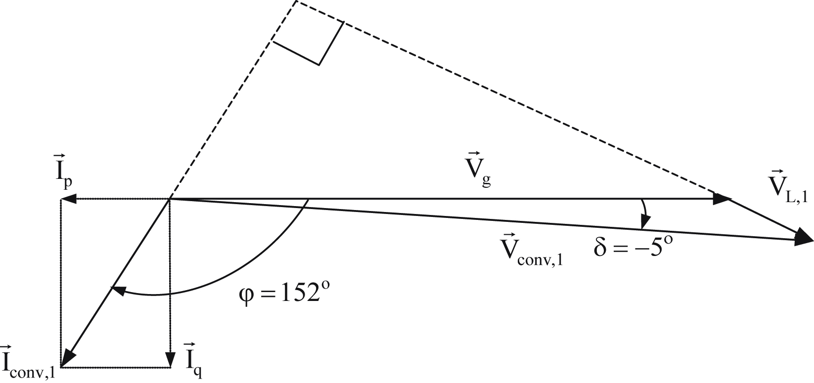
Using Table 6.21 the meaning of the above results is that the grid is feeding active power to the converter and at the same time is absorbing reactive power from the converter (i.e., the utility is acting as a capacitor and the converter as an inductor). According to Fig. 6.138 the system operates in the third quadrant of the Pg–Qg plane and, consequently, the phase angle φ must be between −90° and −180°.
b) According to Eq. (6.215) the rms values of the fundamental component of the line current and its components fed into the utility are given by:


![]()
Since the system operates in the third quadrant of the Pg–Qg plane, the phase angle φ is given by:
![]()
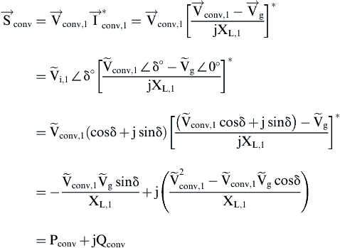
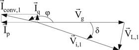
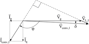
The vector diagram of the system when and converter phase voltage is lagging with respect to the utility phase voltage by 5° will be as given in Fig. 6.143.


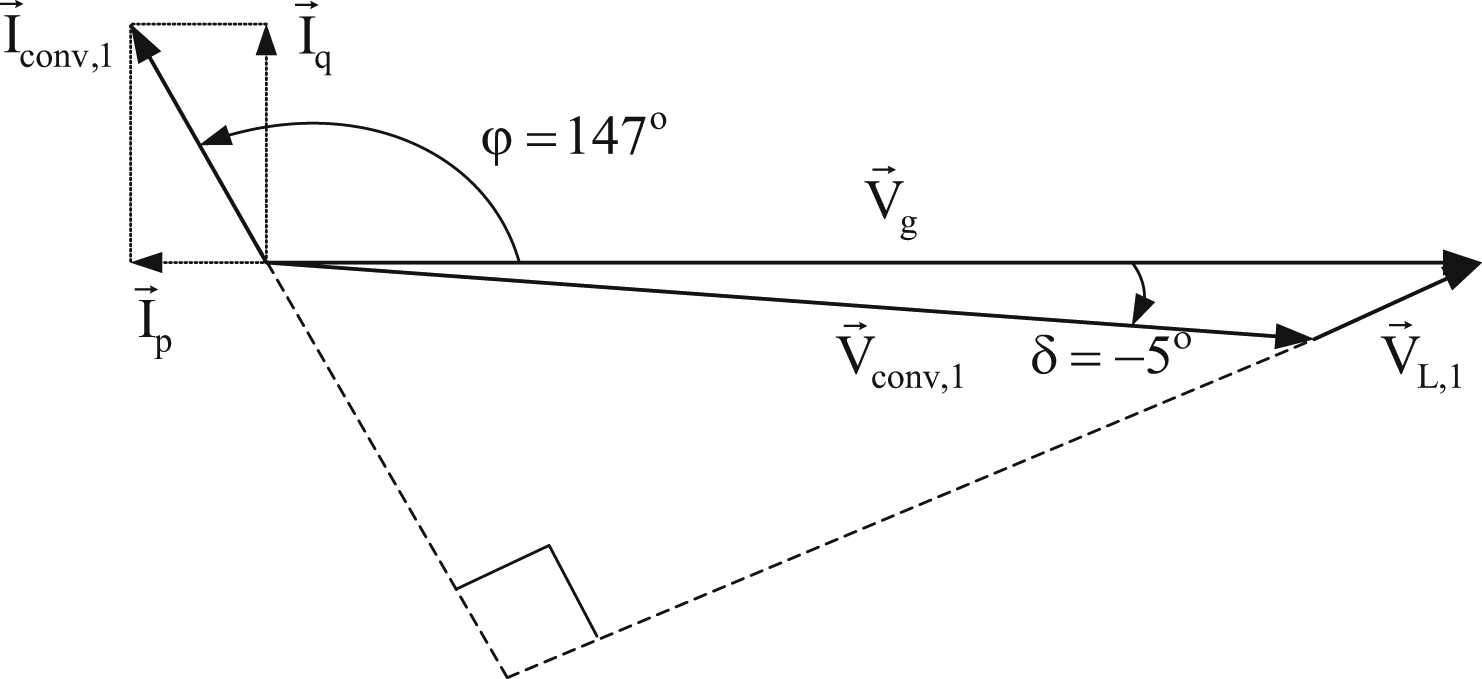
As it was expected since δ has the same value as before the active power remains as in part (a). However, since the utility voltage becomes higher than the inverter voltage, the reactive power will have negative value meaning that the utility will feed reactive power to the converter (i.e., the utility is acting as an inductor and the converter as a capacitor). According to Fig. 6.138 for this mode of operation the system operates in the fourth quadrant of the Pg–Qg plane.
According to Eq. (6.215) the rms values of the fundamental component of the line current and its components fed into the utility are given by:


![]()
Since the system operates in the fourth quadrant of the Pg–Qg plane, the phase angle φ must be in the range of 90° to 180° and is given by:
![]()
The vector diagram of the system when and converter phase voltage is lagging with respect to the utility phase voltage by 5° will be as given in Fig. 6.144.

6.9.1. P–Q Control Based on the Decoupling Control of d–q Current Components
As mentioned before, implementing a control technique in the synchronous rotating frame with d–q dc components eliminates the steady-state errors and exhibits fast transient response. In this section the P–Q control of a three-phase balanced converter, which is based on the decoupling control of d–q current components, will be analyzed.
From Fig. 6.135(a), the following equations hold:
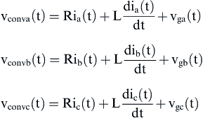 (6.221)
where
vconva, vconvb, vconvc = converter phase voltages with respect to the utility neutral
vga, vgb, vgc = grid phase voltages
ia, ib, ic = converter line currents
L = interconnection inductance
R = interconnection resistance
Applying the Clarke transformation to Eq. (6.221), the following equations are obtained:
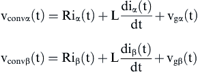 (6.222)
or in matrix form
 (6.223)
or in vector form
![]() (6.224)
(6.224)
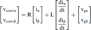
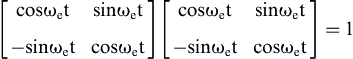
Since the variables vconvα and vconvβ are time variant, they have to be transformed to dc quantities using the Park transformation as follows:
 (6.225)
Using Eq. (6.225) and transforming the variables iα and iβ into dc components and knowing that
the following equation is obtained:
 (6.226)
or
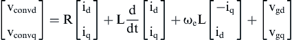 (6.227)
Therefore, assuming that the quantities id and iq are constant, which means that  , and using Eq. (6.227), the d–q components of the inverter output voltages in the synchronous rotating frame are given by:
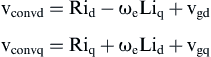 (6.228)
Fig. 6.145 presents the block diagram of a P–Q controller which is based on the SVPWM control technique.
As shown in Fig. 6.145, to synchronize the utility grid with the converter a phase locked loop (PLL) is used which detects the grid phase angle θe = ωet and provides this information to the Park transformation blocks.
For a three-phase balanced system the active and reactive power of the converter expressed with the voltages and currents of the a–b–c reference frame are given by the following equations:
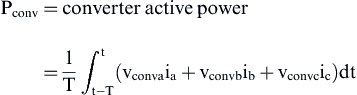 (6.229)
 (6.230)
Transforming the voltages and the currents of Eqs. (6.229) and (6.230) into α–β reference frame yields:
![]() (6.231)
(6.231)
![]() (6.232)
(6.232)
The active and reactive power expressed in voltages and currents of the d–q reference frame must equal the active and reactive power expressed in voltages and currents of the a–b–c reference frame. Therefore, substituting Eq. (6.200) into Eqs. (6.231) and (6.232), the following results are obtained:
![]() (6.233)
(6.233)
![]() (6.234)
(6.234)
where the factor 3/2 is a scaling factor due to the choice of the scaling factor 2/3 used in the transformation Eq. (6.200).
Next, using Eqs. (6.233) and (6.234) the reference currents in the d–q synchronous rotating frame with respect to the reference values  and
and  can be found and are given by the following equations:
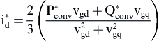 (6.235)
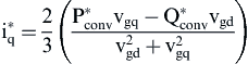 (6.236)
When the converter is synchronized to the utility grid (through the PLL system), the d-axis of the d–q frame is aligned with the vector of the grid voltage . With this alignment, the component vq = 0 and, consequently, control decoupling is achieved and Eqs. (6.233)–(6.236) become:
![]() (6.237)
(6.237)
![]() (6.238)
(6.238)
![]() (6.239)
(6.239)
![]() (6.240)
(6.240)
Therefore, assuming that the utility grid is balanced and stable, the active and reactive power delivered by the converter to the utility grid is determined by the reference currents  , respectively. If the reference current
  , the inverter voltages and currents are in phase and the converter operates at unity power factor.
Solution
The transformation from a–b–c reference frame to α–β is given by:
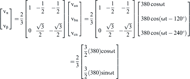
Finally, the transformation from time varying α–β stationary frame to synchronous time invariant d–q frame is given by:
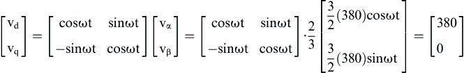
Therefore: vd = 380 V and vq = 0 V.
..................Content has been hidden....................
You can't read the all page of ebook, please click here login for view all page.