
10.8. Mount Package Types of Semiconductor Devices and Types of Heat Sinks
Fig. 10.64 shows different types of mount packages of power semiconductor devices. As can be seen from Fig. 10.64(a), the mount packages TO-220, TO-268, and TO-264 are for low power semiconductor devices. The mount packages shown in Fig. 10.64(b) and (c) are for higher power applications.
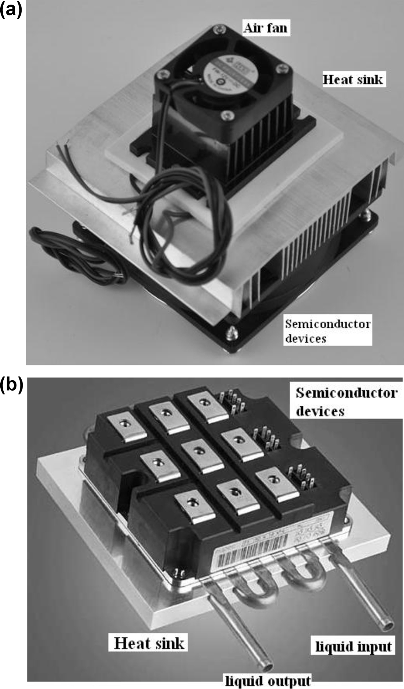
The high power semiconductor switches analyzed in the previous sections, due to the high density of current that flows through their junctions, they exhibit power losses and, consequently, generate internally high temperature levels. Since the high temperature levels are affecting negatively the operation and the life time of the semiconductor devices, there is a need to design a proper heat sink system for temperature dissipation to keep the device under manufacturer's temperature specifications. The aim of the heat sinks is to increase the temperature conductivity between the device module case and the ambient temperature in order for the heat dissipation to become more effective. Fig. 10.65 shows different types of heat sinks that can be used to cool and keep the semiconductor devices to manufacturer's temperature levels. The heat sink is considered to be a natural cooling system.
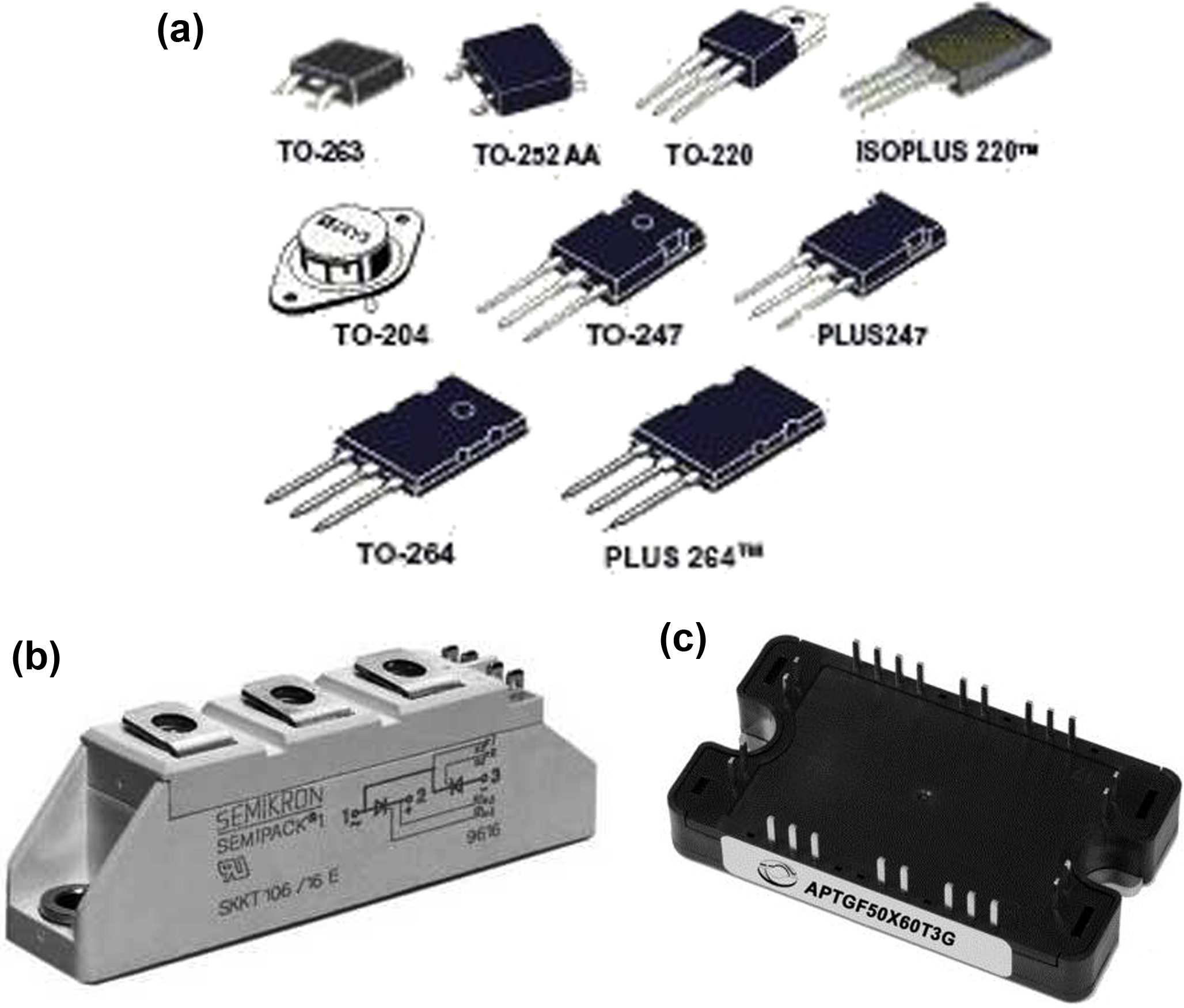
Figure 10.64 Different types of mount packages of power semiconductor switches mount packages.
(a) Single semiconductor switches with different types of mount packages; (b) two-semiconductor switches in one mount package to implement one phase leg; (c) six-semiconductor switches in one mount package to implement three-phase legs.
Fig. 10.66 shows two different heat sinks with natural air cooling for power semiconductor devices.
Besides the natural heat sink air cooling systems there are the so-called heat forced air or liquid cooling techniques which are using air fans or liquid pumps for temperature dissipation. These techniques are applied in applications where the power electronics converter needs high power density. Fig. 10.67 shows two different forced cooling techniques.


10.8.1. Heat Sink Computations
When the power semiconductor devices are operating, they exhibit power switching and conduction losses which are converted to heat. If the junction temperature of the power semiconductor exceeds the manufacturer's specifications the device will be destroyed. Therefore, this high value temperature has to be reduced. The usual way to increase the transfer of excess heat from the crystal of a semiconductor device to the ambient air is to attach the semiconductor device to a heat sink and many times an air fan is also include for faster air flow. The heat sink is made of metal and most of the times from aluminum and is constructed with fins to allow maximum contact with ambient air. The heat flow power is equal to the power losses. The heat flows from the highest temperature region, which is the junction of the crystal, to the lowest, which is the ambient air. The heat flows from the junction to the ambient air through a thermal path consisted of the case of the device, a thermal grease or insulator and a heat sink. Fig. 10.68 shows a heat sink which is used for natural air cooling of four power semiconductor switches.

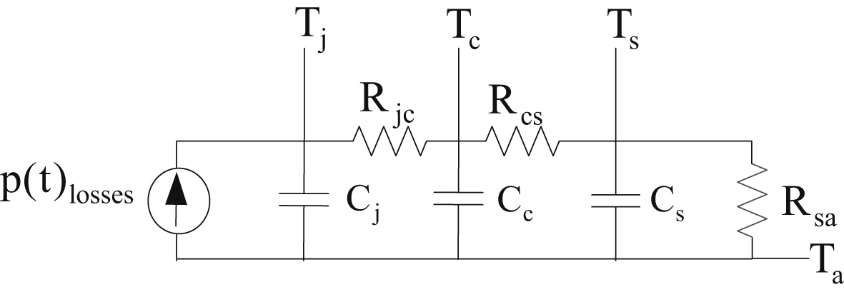
Fig. 10.69(a) shows the direction of the heat flow and the steady-state thermal resistances between different points. Also, Fig. 10.69(b) shows the steady-state thermal resistance equivalent model where the thermal resistance of the thermal grease and the thermal resistance are added to a single thermal resistance case-sink. The power losses of a semiconductor device are equal to the heat transfer power.
To understand the thermal analysis of semiconductor switch mounted on a heat sink Table 10.4 presents how the electrical parameters are associated with the thermal parameters.
To estimate and select the right heat sink for the right application, it is necessary to understand the heat transfer power between two points which is given by:
![]() (10.15)
(10.15)
where Rth = thermal resistance between the two points in °C/W or °K/W (since Rth is based on a temperature difference and not on the absolute temperature, both units are perfectly equivalent (for example, 5°C/W = 5°K/W)); ΔT = Temperature difference (rise).
In case of semiconductor switches that are mounted on a heat sink, the total thermal resistance consists of the following three main components:
1) Thermal resistance, Rjc: It is the thermal resistance between the silicon junction and the case of the semiconductor device. This resistance is given in the manufacturer's specifications.
2) Thermal resistance, Rcs: It is the thermal resistance between the case of the device and the heat sink. This resistance also depends on the thermal grease or insulator that there is between the case and the heat sink. If the thermal grease is applied correctly between the case and the heat sink, then its thermal resistance value is negligible and can be ignored. The thermal resistance of an insulator is provided by the manufacturer.
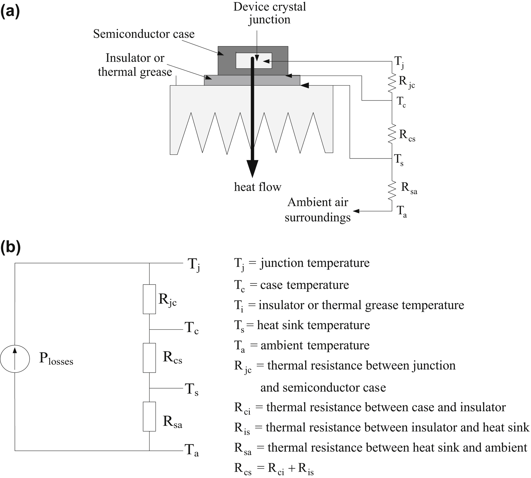
Figure 10.69 Heat sink thermal resistances for single semiconductor device.
(a) Heat flow through a heat sink and thermal resistances between different points; (b) steady-state thermal resistances equivalent model.
Table 10.4
Association between electrical and thermal parameters
Electrical parameters 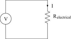 Rel = electrical resistance (Ω) V = potential difference (V) I = electrical current V = I × Rel | Thermal parameters 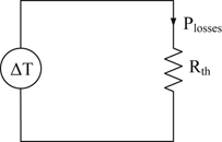 Rth = thermal resistance (°C/W or °K/W) ΔΤ = temperature difference (°C or °K) Ρlosses = power losses of the semiconductor device (W) ΔT = Ρlosses × Rth (°C) |
3) Thermal resistance, Rsa: It is the thermal resistance between the heat sink and the ambient temperature. This resistance depends on the characteristics of the heat sink (i.e., material, color, shape, and dimensions).
Therefore, the total steady-state (i.e., constant power losses) thermal resistance between the junction and the ambient air is given by:
![]() (10.16)
(10.16)
where Tjmax = maximum junction temperature; Ta = ambient air temperature; Plosses(av) = maximum permissible power average losses of the semiconductor device.
Also, from Fig. 10.69(b), the following equations can be obtained:
 (10.17)
![]() (10.18)
(10.18)
![]() (10.19)
(10.19)
![]() (10.20)
(10.20)
![]() (10.21)
(10.21)
Solution
![]()
![]()
Solution
Solution
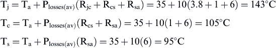
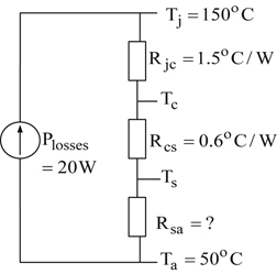
Using the above given specifications the following steady-state thermal resistances equivalent model is obtained:
![]()

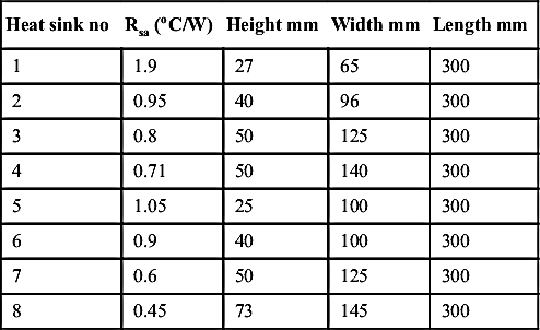
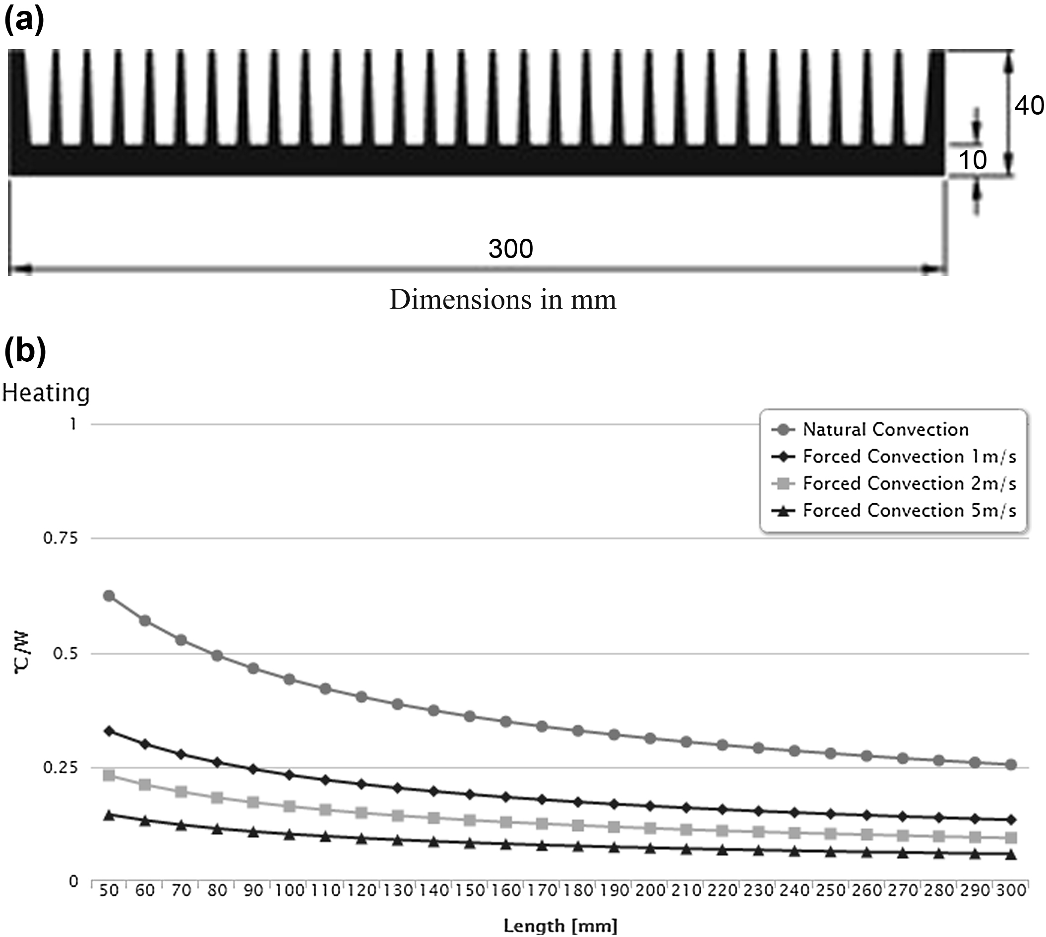
Figure 10.70 Different types of heat sinks and their respective specifications given in Table 10.5.
(Courtecy of BAL GROUP Ltd).
Therefore to keep the device junction to 150°C the device should be mounted on a heat sink with thermal resistance of 1.9°C/W. From the heat sinks of Fig. 10.70 and according to their specifications, which are given in Table 10.5, the best choice is the heat sink no. 1.
Table 10.5
Specifications of the aluminum type heat sinks shown in Figure 10.71
| Heat sink no | Rsa (oC/W) | Height mm | Width mm | Length mm |
| 1 | 1.9 | 27 | 65 | 300 |
| 2 | 0.95 | 40 | 96 | 300 |
| 3 | 0.8 | 50 | 125 | 300 |
| 4 | 0.71 | 50 | 140 | 300 |
| 5 | 1.05 | 25 | 100 | 300 |
| 6 | 0.9 | 40 | 100 | 300 |
| 7 | 0.6 | 50 | 125 | 300 |
| 8 | 0.45 | 73 | 145 | 300 |
Solution
![]()
Therefore, from the heat sinks of Fig. 10.70 the best choice is the heat sink no. 5.
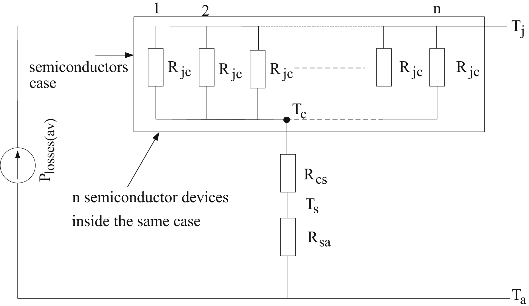
When multiple power semiconductor devices are mounted on a common heat sink, their thermal resistance model can be one of the models shown in Figs. 10.71 and 10.72. Fig. 10.71 presents the thermal resistance steady-state model when the power semiconductor devices have individual mounting case and Fig. 10.72 presents the thermal resistance steady-state model when the power semiconductor devices have common mounting case.
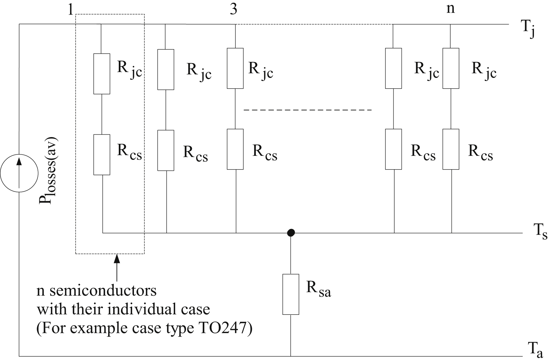
According to Fig. 10.71, when power semiconductors have individual mounting case and are mounted on a heat sink then the total thermal resistance of the heat sink is given by:
![]() (10.22)
(10.22)
Also, according to Fig. 10.72, when power semiconductors have common case the total thermal resistance of the heat sink is given by:
![]() (10.23)
(10.23)
where n is the number of semiconductor devices.
Solution
Using the thermal model of Fig. 10.71, the following thermal resistance model is obtained.
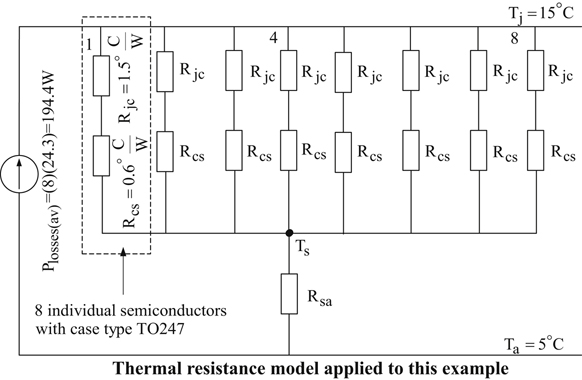
Using Eq. (10.22), the following results are obtained:
![]()
![]()
Therefore to maintain the junction temperature of the semiconductor devices Tj ≤ 150°C they have to be mounted on a heat sink that will have thermal resistance of Rsa ≤ 0.255°C/W. Fig. 10.73 presents a proposed heat sink and the respective air flow speed characteristics.
Company: Birmingham Aluminum
Series: 1500 series
Length: 300 mm
Thermal resistance: 0.255°C/W
The steady-state thermal resistance is not enough for finding peak junction temperatures for pulsed current applications. Using the peak power value, results in overestimating the actual junction temperature, while using the average power value underestimates the peak junction temperature at the end of the power pulse. The reason for the discrepancy lies in the thermal capacity of the semiconductor and its housing (i.e., its ability to store heat and to cool down before the next current pulse). Fig. 10.74 presents the modified thermal equivalent circuit when transient thermal analysis is needed.
The normally distributed thermal capacitances have been lumped into single capacitors labeled Cj, Cc, and Cs. This simplification assumes current is evenly distributed across the silicon crystal and that the only significant power losses occur in the junction. When a step of heating power, Plosses(max), is introduced at the junction of the semiconductor, Tj will rise exponentially to some steady-state value dependent upon the response of the thermal network. When in a time instant the current pulse becomes zero and, consequently, the power losses become zero, Tj will decrease exponentially until the next current pulse. The transient thermal impedance between junction and case at time t is given by:
![]() (10.24)
(10.24)
where ΔTjc(t) = difference of temperature between junction and case at a given time t; Plosses(max) = amplitude of the step power losses.
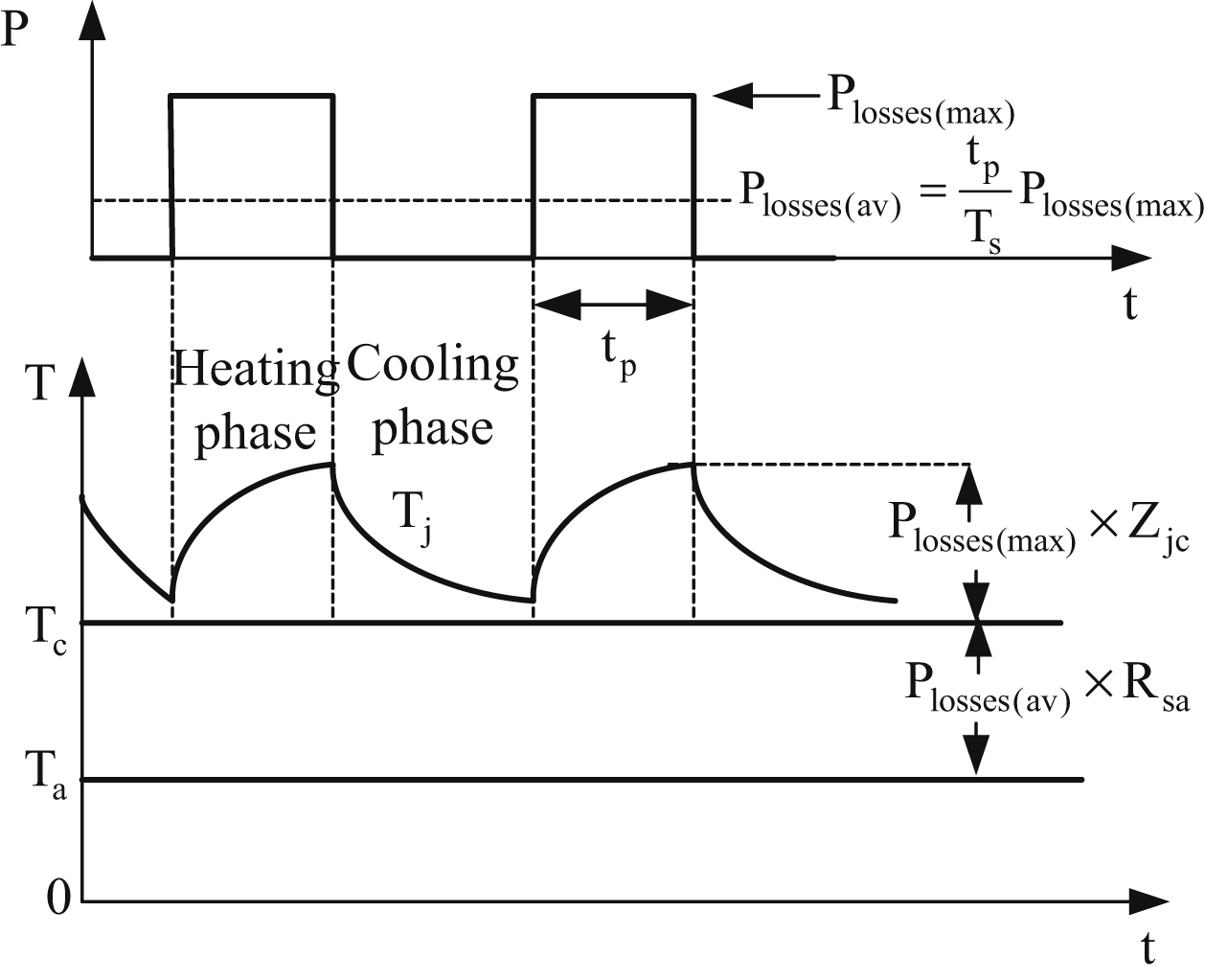
Figure 10.75 Variation of junction and case temperature when the pulse time is small compared to thermal time constant of the heat sink.
The junction to case temperature is always assumed to be constant under transient operation. This is valid in practice when the power pulse width is less than about 1 s. As can be seen from Fig. 10.75, Tjc does not change significantly under this condition. This is because heat sinks have a high thermal capacity and, consequently, a high thermal time constant. Thus, Eq. (10.24) is valid for transient operation when the pulse time is less than 1 s. Therefore, using Eq. (10.24) the value of Tj can be calculated as follows:
![]() (10.25)
(10.25)
If the power pulse width tp exceeds 1 s (see Fig. 10.76), the semiconductor device is temporarily in thermal equilibrium since such a pulse width is significantly greater than the thermal time constant of the semiconductor. Therefore, in this case Eq. (10.24) becomes:
![]() (10.26)
(10.26)
The following expression describes how to select the heat sink that keeps the junction at/or below a given temperature:
![]() (10.27)
(10.27)
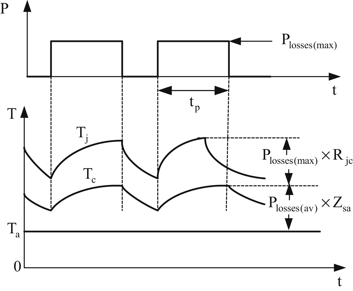
Figure 10.76 Variation of junction and case temperature when the pulse time is not small compared to thermal time constant of the heat sink.
Example 10.7
Calculate the junction temperature of the IGBT type SGP20N60 under the following operating conditions:
D = duty cycle = 0.5
fs = switching frequency = 75 kHz
Ta = ambient temperature = 40°C
Tc = case temperature = 80°C
Plosses(max) = 45 W
Rcs = thermal resistance between case and heat sink = 0.45
Fig. 10.77 presents the thermal impedance of the IGBT type SGP20N60 for different duty cycles given by the manufacturer.
Solution
Since the operating duty cycle is 0.5 and the switching frequency 75 kHz, then the pulse width of the power losses is given by:
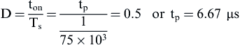

From Fig. 10.77, for tp = 6.67 μs and D = 0.5 the thermal impedance is  . At this point it should be mentioned that
  . Therefore using Eqs. (10.26) and (10.27), the following results are obtained:
![]()
![]()
Therefore, from the heat sinks of Fig. 10.70 according to their specifications, which are given in Table 10.5, the best choice is a heat sink with higher dimensions of no. 8.
Example 10.8
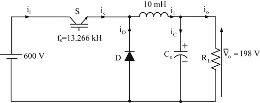
For the step-down converter shown below, the following parameters are given:
IGBT
Conduction voltage = 2 V
Conduction resistance = 3 mΩ
Won = 20 mJ (measured at 400 A with 600 V dc supply)
Woff = 40 mJ (measured at 400 A with 600 V dc supply)
Thermal resistance junction case 0.05°K/W
Diode
Conduction voltage = 2.5 V
Conduction resistance = 2 mΩ
Thermal resistance junction case = 0.1°K/W
a) Calculate the power dissipated in the IGBT and diode.
b) Estimate the junction temperature of the IGBT and diode for a case temperature of 60°C.
Solution
![]()
![]()
Assuming that the semiconductor switch operates with a duty cycle D = 0.33 and switching frequency 13.266 kHz, then the power losses of the IGBT are:
![]()
![]()
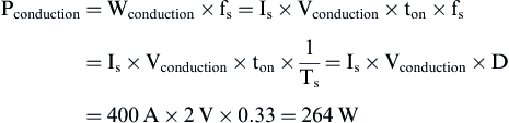
Therefore, the total power losses of the IGBT are:
![]()
Moreover, the power losses of the diode are calculated as follows:

The conduction losses of the diode are given by:
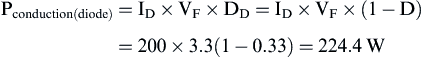
where DD = diode duty cycle.
Also, it is known that:
![]()
Therefore, the junction temperature of a semiconductor device is given by:
![]()
Therefore, the junction temperature of the IGBT is:
![]()
and the junction temperature of the diode is:
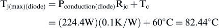
The total power that a power device can dissipate is based on the maximum junction temperature and the thermal resistance Rθjc at a case temperature of 25°C.
..................Content has been hidden....................
You can't read the all page of ebook, please click here login for view all page.