Chapter 3. Communication Concepts
The design of highly-integrated RF transceivers requires a solid understanding of communication theory. For example, as mentioned in Chapter 2, the receiver sensitivity depends on the minimum acceptable signal-to-noise ratio, which itself depends on the type of modulation. In fact, today we rarely design a low-noise amplifier, an oscillator, etc., with no attention to the type of transceiver in which they are used. Furthermore, modern RF designers must regularly interact with digital signal processing engineers to trade functions and specifications and must therefore speak the same language.
This chapter provides a basic, yet necessary, understanding of modulation theory and wireless standards. Tailored to a reader who is ultimately interested in RF IC design rather than communication theory, the concepts are described in an intuitive language so that they can be incorporated in the reader’s daily work. The outline of the chapter is shown below.
3.1 General Considerations
How does your voice enter a cell phone here and come out of another cell phone miles away? We wish to understand the incredible journey that your voice signal takes.
The transmitter in a cell phone must convert the voice, which is called a “baseband signal” because its spectrum (20 Hz to 20 kHz) is centered around zero frequency, to a “passband signal,” i.e., one residing around a nonzero center frequency, ωc [Fig. 3.1(b)]. We call ωc the “carrier frequency.”
Figure 3.1 (a) Baseband and (b) passband signal spectra.
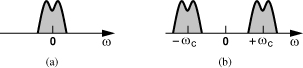
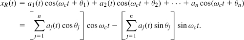
More generally, “modulation” converts a baseband signal to a passband signal. From another point of view, modulation varies certain parameters of a sinusoidal carrier according to the baseband signal. For example, if the carrier is expressed as A0 cos ωct, then the modulated signal is given by
![]()
where the amplitude, a(t) and the phase, θ(t), are modulated.
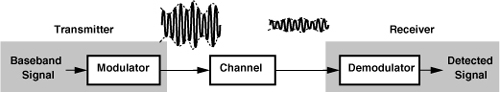
The inverse of modulation is demodulation or detection, with the goal being to reconstruct the original baseband signal with minimal noise, distortion, etc. Thus, as depicted in Fig. 3.2, a simple communication system consists of a modulator/transmitter, a channel (e.g., air or a cable), and a receiver/demodulator. Note that the channel attenuates the signal. A “transceiver” contains both a modulator and a demodulator; the two are called a “modem.”
Figure 3.2 Generic communication system.
Important Aspects of Modulation
Among various attributes of each modulation scheme, three prove particularly critical in RF design.
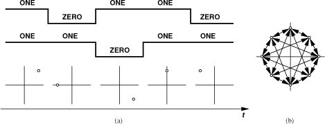
1. Detectability, i.e., the quality of the demodulated signal for a given amount of channel attenuation and receiver noise. As an example, consider the binary amplitude modulation shown in Fig. 3.3(a), where logical ONEs are represented by full amplitude and ZEROs by zero amplitude. The demodulation must simply distinguish between these two amplitude values. Now, suppose we wish to carry more information and hence employ four different amplitudes as depicted in Fig. 3.3(b).
Figure 3.3 (a) Two-level and (b) four-level modulation schemes.

In this case, the four amplitude values are closer to one another and can therefore be misinterpreted in the presence of noise. We say the latter signal is less detectable.
2. Bandwidth efficiency, i.e., the bandwidth occupied by the modulated carrier for a given information rate in the baseband signal. This aspect plays a critical role in today’s systems because the available spectrum is limited. For example, the GSM phone system provides a total bandwidth of 25 MHz for millions of users in crowded cities. The sharing of this bandwidth among so many users is explained in Section 3.6.
3. Power efficiency, i.e., the type of power amplifier (PA) that can be used in the transmitter. As explained later in this chapter, some modulated waveforms can be processed by means of nonlinear power amplifiers, whereas some others require linear amplifiers. Since nonlinear PAs are generally more efficient (Chapter 12), it is desirable to employ a modulation scheme that lends itself to nonlinear amplification.
The above three attributes typically trade with one another. For example, we may suspect that the modulation format in Fig. 3.3(b) is more bandwidth-efficient than that in Fig. 3.3(a) because it carries twice as much information for the same bandwidth. This advantage comes at the cost of detectability—because the amplitude values are more closely spaced—and power efficiency—because PA nonlinearity compresses the larger amplitudes.
3.2 Analog Modulation
If an analog signal, e.g., that produced by a microphone, is impressed on a carrier, then we say we have performed analog modulation. While uncommon in today’s high-performance communications, analog modulation provides fundamental concepts that prove essential in studying digital modulation as well.
3.2.1 Amplitude Modulation
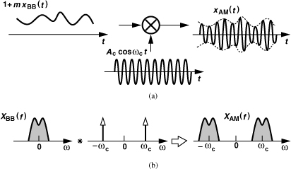
For a baseband signal xBB(t), an amplitude-modulated (AM) waveform can be constructed as
![]()
where m is called the “modulation index.”1 Illustrated in Fig. 3.4(a) is a multiplication method for generating an AM signal. We say the baseband signal is “upconverted.” The waveform Ac cos ωct is generated by a “local oscillator” (LO). Multiplication by cos ωct in the time domain simply translates the spectrum of xBB(t) to a center frequency of ωc [Fig. 3.4(b)]. Thus, the bandwidth of xAM(t) is twice that of xBB(t). Note that since xBB(t) has a symmetric spectrum around zero (because it is a real signal), the spectrum of xAM(t) is also symmetric around ωc. This symmetry does not hold for all modulation schemes and plays a significant role in the design of transceiver architectures (Chapter 4).
Figure 3.4 (a) Generation of AM signal, (b) resulting spectra.
Except for broadcast AM radios, amplitude modulation finds limited use in today’s wireless systems. This is because carrying analog information in the amplitude requires a highly-linear power amplifier in the transmitter. Amplitude modulation is also more sensitive to additive noise than phase or frequency modulation is.
3.2.2 Phase and Frequency Modulation
Phase modulation (PM) and frequency modulation (FM) are important concepts that are encountered not only within the context of modems but also in the analysis of such circuits as oscillators and frequency synthesizers.
Let us consider Eq. (3.1) again. We call the argument ωct + θ(t) the “total phase.” We also define the “instantaneous frequency” as the time derivative of the phase; thus, ωc + dθ/dt is the “total frequency” and dθ/dt is the “excess frequency” or the “frequency deviation.” If the amplitude is constant and the excess phase is linearly proportional to the baseband signal, we say the carrier is phase-modulated:
![]()
where m denotes the phase modulation index. To understand PM intuitively, first note that, if xBB(t) = 0, then the zero-crossing points of the carrier waveform occur at uniformly-spaced instants equal to integer multiples of the period, Tc = 1/ωc. For a time-varying xBB(t), on the other hand, the zero crossings are modulated (Fig. 3.6) while the amplitude remains constant.
Figure 3.6 Zero crossings in a phase-modulated signal.

Similarly, if the excess frequency, dθ/dt, is linearly proportional to the baseband signal, we say the carrier is frequency-modulated:
Note that the instantaneous frequency is equal to ωc + mxBB(t).2
The nonlinear dependence of xPM(t) and xFM(t) upon xBB(t) generally increases the occupied bandwidth. For example, if xBB(t) = Am cos ωmt, then
![]()
exhibiting spectral lines well beyond ωc ± ωm. Various approximations for the bandwidth of PM and FM signals have been derived [1–3].
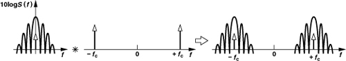
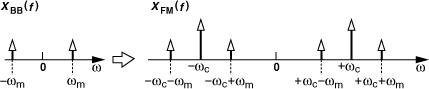
Narrowband FM Approximation
A special case of FM that proves useful in the analysis of RF circuits and systems arises if mAm/ωm ![]() 1 rad in Eq. (3.12). The signal can then be approximated as
1 rad in Eq. (3.12). The signal can then be approximated as

Illustrated in Fig. 3.7, the spectrum consists of impulses at ±ωc (the carrier) and “sidebands” at ωc ± ωm and −ωc ± ωm. Note that, as the modulating frequency, ωm, increases, the magnitude of the sidebands decreases.
Figure 3.7 Spectrum of a narrowband FM signal.
Solution:
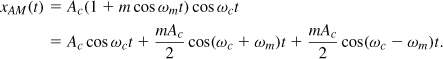
Figure 3.8 Spectra of (a) narrowband FM and (b) AM signals.

Figure 3.9 Spectra of AM and narrowband FM signals.
Figure 3.10 Rotation of (a) AM and (b) FM sidebands with respect to the carrier.

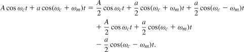
The insights afforded by the above example prove useful in many RF circuits. The following example shows how an interesting effect in nonlinear circuits can be explained with the aid of the foregoing observations.
Figure 3.11 (a) Differential pair sensing a large and a small signal, (b) conversion of one sideband to AM and FM components.
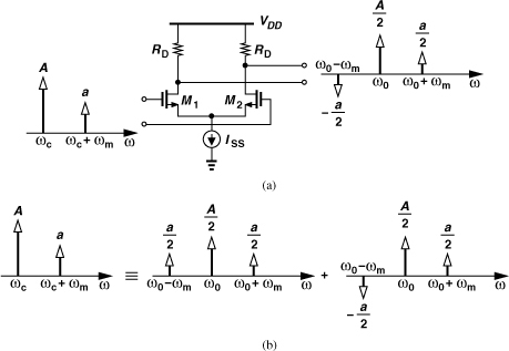
Solution:
3.3 Digital Modulation
In digital communication systems, the carrier is modulated by a digital baseband signal. For example, the voice produced by the microphone in a cell phone is digitized and subsequently impressed on the carrier. As explained later in this chapter, carrying the information in digital form offers many advantages over communication in the analog domain.
The digital counterparts of AM, PM, and FM are called “amplitude shift keying” (ASK), “phase shift keying” (PSK), and “frequency shift keying” (FSK), respectively. Figure 3.12 illustrates examples of these waveforms for a binary baseband signal. A binary ASK signal toggling between full and zero amplitudes is also known as “on-off keying” (OOK). Note that for the PSK waveform, the phase of the carrier toggles between 0 and 180°:
![]()
Figure 3.12 ASK, PSK, and FSK waveforms.

It is instructive to consider a method of generating ASK and PSK signals. As shown in Fig. 3.13(a), if the baseband binary data toggles between 0 and 1, then the product of this waveform and the carrier yields an ASK output. On the other hand, as depicted in Fig. 3.13(b), if the baseband data toggles between −0.5 and +0.5 (i.e., it has a zero average), then the product of this waveform and the carrier produces a PSK signal because the sign of the carrier must change (and hence the phase jumps by 180°) every time the data changes.
Figure 3.13 Generation of (a) ASK and (b) PSK signals.

In addition to ASK, PSK, and FSK, numerous other digital modulation schemes have been introduced. In this section, we study those that find wide application in RF systems. But, we must first familiarize ourselves with two basic concepts in digital communications: “intersymbol interference” (ISI) and “signal constellations.”
3.3.1 Intersymbol Interference
Linear time-invariant systems can “distort” a signal if they do not provide sufficient bandwidth. A familiar example of such a behavior is the attenuation of high-frequency components of a periodic square wave in a low-pass filter [Fig. 3.14(a)]. However, limited bandwidth more detrimentally impacts random bit streams. To understand the issue, first recall that if a single ideal rectangular pulse is applied to a low-pass filter, then the output exhibits an exponential tail that becomes longer as the filter bandwidth decreases. This occurs fundamentally because a signal cannot be both time-limited and bandwidth-limited: when the time-limited pulse passes through the band-limited system, the output must extend to infinity in the time domain.
Figure 3.14 Effect of low-pass filter on (a) periodic waveform and (b) random sequence.
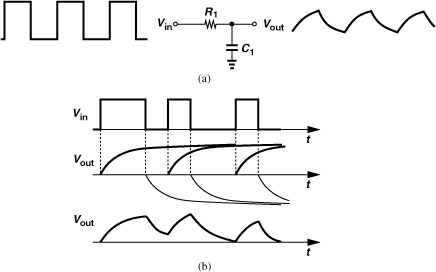
Now suppose the output of a digital system consists of a random sequence of ONEs and ZEROs. If this sequence is applied to a low-pass filter (LPF), the output can be obtained as the superposition of the responses to each input bit [Fig. 3.14(b)]. We note that each bit level is corrupted by decaying tails created by previous bits. Called “intersymbol interference” (ISI), this phenomenon leads to a higher error rate because it brings the peak levels of ONEs and ZEROs closer to the detection threshold. We also observe a trade-off between noise and ISI: if the bandwidth is reduced so as to lessen the integrated noise, then ISI increases.
In general, any system that removes part of the spectrum of a signal introduces ISI. This can be better seen by an example.

Let us continue our thought process and determine the spectrum if the binary sequence shown in Fig. 3.15(a) is impressed on the phase of a carrier. From the generation method of Fig. 3.13(b), we write
![]()
concluding that the upconversion operation shifts the spectrum of xBB(t) to ±fc = ±ωc/(2π) (Fig. 3.16). From Fig. 3.13(a) and Example 3.1, we also recognize that the spectrum of an ASK waveform is similar but with impulses at ±fc.
Figure 3.16 Spectrum of PSK signal.

Pulse Shaping
The above analysis suggests that, to reduce the bandwidth of the modulated signal, the baseband pulse must be designed so as to occupy a small bandwidth itself. In this regard, the rectangular pulse used in the binary sequence of Fig. 3.15(a) is a poor choice: the sharp transitions between ZEROs and ONEs lead to an unnecessarily wide bandwidth. For this reason, the baseband pulses in communication systems are usually “shaped” to reduce their bandwidth. Shown in Fig. 3.17 is a conceptual example where the basic pulse exhibits smooth transitions, thereby occupying less bandwidth than rectangular pulses.
Figure 3.17 Effect of smooth data transitions on spectrum.
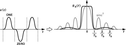
What pulse shape yields the tightest spectrum? Since the spectrum of an ideal rectangular pulse is a sinc, we surmise that a sinc pulse in the time domain gives a rectangular (“brickwall”) spectrum [Fig. 3.18(a)]. Note that the spectrum is confined to ±1/(2Tb). Now, if a random binary sequence employs such a pulse every Tb seconds, from Eq. (3.21) the spectrum still remains a rectangle [Fig. 3.18(b)] occupying substantially less bandwidth than Sx(f) in Fig. 3.15(b). This bandwidth advantage persists after upconversion as well.
Figure 3.18 (a) Sinc pulse and its spectrum, (b) random sequence of sinc pulses and its spectrum.

Do we observe ISI in the random waveform of Fig. 3.18(b)? If the waveform is sampled at exactly integer multiples of Tb, then ISI is zero because all other pulses go through zero at these points. The use of such overlapping pulses that produce no ISI is called “Nyquist signaling.” In practice, sinc pulses are difficult to generate and approximations are used instead. A common pulse shape is shown in Fig. 3.19(a) and expressed as
![]()
Figure 3.19 Raised-cosine pulse shaping: (a) basic pulse and (b) corresponding spectrum.

This pulse exhibits a “raised-cosine” spectrum [Fig. 3.19(b)]. Called the “roll-off factor,” α determines how close p(t) is to a sinc and, hence, the spectrum to a rectangle. For α = 0, the pulse reduces to a sinc whereas for α = 1, the spectrum becomes relatively wide. Typical values of α are in the range of 0.3 to 0.5.
3.3.2 Signal Constellations
“Signal constellations” allow us to visualize modulation schemes and, more importantly, the effect of nonidealities on them. Let us begin with the binary PSK signal expressed by Eq. (3.24), which reduces to
![]()
for rectangular baseband pulses. We say this signal has one “basis function,” cos ωct, and is simply defined by the possible values of the coefficient, an. Shown in Fig. 3.20(a), the constellation represents the values of an. The receiver must distinguish between these two values so as to decide whether the received bit is a ONE or a ZERO. In the presence of amplitude noise, the two points on the constellation become “fuzzy” as depicted in Fig. 3.20(b), sometimes coming closer to each other and making the detection more prone to error.
Figure 3.20 Signal constellation for (a) ideal and (b) noisy PSK signal.
![]()

Next, we consider an FSK signal, which can be expressed as
![]()
We say cos ω1t and cos ω2t are the basis functions4 and plot the possible values of a1 and a2 as in Fig. 3.22(a). An FSK receiver must decide whether the received frequency is ω1 (i.e., a1 = 1, a2 = 0) or ω2 (i.e., a1 = 0, a2 = 1). In the presence of noise, a “cloud” forms around each point in the constellation [Fig. 3.22(b)], causing an error if a particular sample crosses the decision boundary.
Figure 3.22 Constellation of (a) ideal and (b) noisy FSK signal.
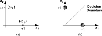
A comparison of the constellations in Figs. 3.20(b) and 3.22(b) suggests that PSK signals are less susceptible to noise than are FSK signals because their constellation points are farther from each other. This type of insight makes constellations a useful tool in analyzing RF systems.
The constellation can also provide a quantitative measure of the impairments that corrupt the signal. Representing the deviation of the constellation points from their ideal positions, the “error vector magnitude” (EVM) is such a measure. To obtain the EVM, a constellation based on a large number of detected samples is constructed and a vector is drawn between each measured point and its ideal position (Fig. 3.23). The EVM is defined as the rms magnitude of these error vectors normalized to the signal rms voltage:
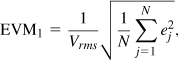
where ej denotes the magnitude of each error vector and Vrms the rms voltage of the signal. Alternatively, we can write

where Pavg is the average signal power. Note that to express EVM in decibels, we compute 20 log EVM1 or 10 log EVM2.
Figure 3.23 Illustration of EVM.

The signal constellation and the EVM form a powerful tool for analyzing the effect of various nonidealities in the transceiver and the propagation channel. Effects such as noise, nonlinearity, and ISI readily manifest themselves in both.
3.3.3 Quadrature Modulation
Recall from Fig. 3.16 that binary PSK signals with square baseband pulses of width Tb seconds occupy a total bandwidth quite wider than 2/Tb hertz (after upconversion to RF). Baseband pulse shaping can decrease this bandwidth to about 2/Tb.
In order to further reduce the bandwidth, “quadrature modulation,” more specifically, “quadrature PSK” (QPSK) modulation can be performed. Illustrated in Fig. 3.24, the idea is to subdivide a binary data stream into pairs of two consecutive bits and impress these bits on the “quadrature phases” of the carrier, i.e., cos ωct and sin ωct:
![]()
Figure 3.24 Generation of QPSK signal.

As shown in Fig. 3.24, a serial-to-parallel (S/P) converter (demultiplexer) separates the even-numbered bits, b2m, and odd-numbered bits, b2m+1, applying one group to the upper arm and the other to the lower arm. The two groups are then multiplied by the quadrature components of the carrier and subtracted at the output. Since cos ωct and sin ωct are orthogonal, the signal can be detected uniquely and the bits b2m and b2m+1 can be separated without corrupting each other.
QPSK modulation halves the occupied bandwidth. This is simply because, as shown in Fig. 3.24, the demultiplexer “stretches” each bit duration by a factor of two before giving it to each arm. In other words, for a given pulse shape and bit rate, the spectra of PSK and QPSK are identical except for a bandwidth scaling by a factor of two. This is the principal reason for the widespread usage of QPSK. To avoid confusion, the pulses that appear at A and B in Fig. 3.24 are called “symbols” rather than bits.5 Thus, the “symbol rate” of QPSK is half of its bit rate.
To obtain the QPSK constellation, we assume bits b2m and b2m+1 are pulses with a height of ±1 and write the modulated signal as x(t) = α1Ac cos ωct + α2Ac sin ωct, where α1 and α2 can each take on a value of +1 or −1. The constellation is shown in Fig. 3.25(a). More generally, the pulses appearing at A and B in Fig. 3.24 are called “quadrature baseband signals” and denoted by I (for “in-phase”) and Q (for quadrature). For QPSK, I = α1Ac and Q = α2Ac, yielding the constellation in Fig. 3.25(b). In this representation, too, we may simply plot the values of α1 and α2 in the constellation.
Figure 3.25 QPSK signal constellation in terms of (a) α1 and α2, and (b) quadrature phases of carrier.

An important drawback of QPSK stems from the large phase changes at the end of each symbol. As depicted in Fig. 3.27, when the waveforms at the output of the S/P converter change simultaneously from, say, [−1 − 1] to [+1 + 1], the carrier experiences a 180° phase step, or equivalently, a transition between two diagonally opposite points in the constellation. To understand why this is a serious issue, first recall from Section 3.3.1 that the baseband pulses are usually shaped so as to tighten the spectrum. What happens if the symbol pulses at nodes A and B are shaped before multiplication by the carrier phases? As illustrated in Fig. 3.28, with pulse shaping, the output signal amplitude (“envelope”) experiences large changes each time the phase makes a 90° or 180° transition. The resulting waveform is called a “variable-envelope signal.” We also note the envelope variation is proportional to the phase change. As explained in Section 3.4, a variable-envelope signal requires a linear power amplifier, which is inevitably less efficient than a nonlinear PA.
Figure 3.27 Phase transitions in QPSK signal due to simultaneous transitions at A and B.

Figure 3.28 QPSK waveform with (a) square baseband pulses and (b) shaped baseband pulses.

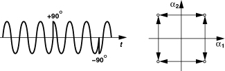
A variant of QPSK that remedies the above drawback is “offset QPSK” (OQPSK). As shown in Fig. 3.29, the data streams are offset in time by half the symbol period after S/P conversion, thereby avoiding simultaneous transitions in waveforms at nodes A and B. The phase step therefore does not exceed ±90°. Figure 3.30 illustrates the phase transitions in the time domain and in the constellation. This advantage is obtained while maintaining the same spectrum. Unfortunately, however, OQPSK does not lend itself to “differential encoding” (Section 3.8). This type of encoding finds widespread usage as it obviates the need for “coherent detection,” a difficult task.
Figure 3.29 Offset QPSK modulator.

Figure 3.30 Phase transitions in OQPSK.
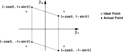
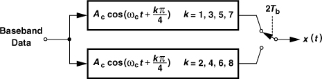
A variant of QPSK that can be differentially encoded is “π/4-QPSK” [4, 5]. In this case, the signal set consists of two QPSK schemes, one rotated 45° with respect to the other:
![]()
![]()
As shown in Fig. 3.31, the modulation is performed by alternately taking the output from each QPSK generator.
Figure 3.31 Conceptual generation of π/4-QPSK signal.
To better understand the operation, let us study the simple π/4-QPSK generator shown in Fig. 3.32. After S/P conversion, the digital signal levels are scaled and shifted so as to present ±1 in the upper QPSK modulator and 0 and ![]() in the lower. The outputs are therefore equal to x1(t) = α1 cos ωct + α2 sin ωct, where [α1 α2] = [±Ac ±Ac], and x2(t) = β1 cos ωct + β2 sin ωct, where
in the lower. The outputs are therefore equal to x1(t) = α1 cos ωct + α2 sin ωct, where [α1 α2] = [±Ac ±Ac], and x2(t) = β1 cos ωct + β2 sin ωct, where ![]() and
and ![]() . Thus, the constellation alternates between the two depicted in Fig. 3.32. Now consider a baseband sequence of [11, 01, 10, 11, 01]. As shown in Fig. 3.33, the first pair, [1 1], is converted to [+Ac + Ac] in the upper arm, producing y(t) = Ac cos(ωct + π/4). The next pair, [0 1], is converted to
. Thus, the constellation alternates between the two depicted in Fig. 3.32. Now consider a baseband sequence of [11, 01, 10, 11, 01]. As shown in Fig. 3.33, the first pair, [1 1], is converted to [+Ac + Ac] in the upper arm, producing y(t) = Ac cos(ωct + π/4). The next pair, [0 1], is converted to ![]() in the lower arm, yielding
in the lower arm, yielding ![]() . Following the values of y(t) for the entire sequence, we note that the points chosen from the two constellations appear as in Fig. 3.33(a) as a function of time. The key point here is that, since no two consecutive points are from the same constellation, the maximum phase step is 135°, 45° less than that in QPSK. This is illustrated in Fig. 3.33(b). Thus, in terms of the maximum phase change, π/4-QPSK is an intermediate case between QPSK and OQPSK.
. Following the values of y(t) for the entire sequence, we note that the points chosen from the two constellations appear as in Fig. 3.33(a) as a function of time. The key point here is that, since no two consecutive points are from the same constellation, the maximum phase step is 135°, 45° less than that in QPSK. This is illustrated in Fig. 3.33(b). Thus, in terms of the maximum phase change, π/4-QPSK is an intermediate case between QPSK and OQPSK.
Figure 3.32 Generation of π/4-QPSK signals.
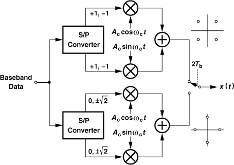
Figure 3.33 (a) Evolution of π/4-QPSK in time domain, (b) possible phase transitions in the constellation.
By virtue of baseband pulse shaping, QPSK and its variants provide high spectral efficiency but lead to poor power efficiency because they dictate linear power amplifiers. These modulation schemes are used in a number of applications (Section 3.7).
3.3.4 GMSK and GFSK Modulation
A class of modulation schemes that does not require linear power amplifiers, thus exhibiting high power efficiency, is “constant-envelope modulation.” For example, an FSK waveform expressed as xFSK(t) = Ac cos[ωct + m ![]() xBB(t)dt] has a constant envelope. To arrive at variants of FSK, let us first consider the implementation of a frequency modulator. As illustrated in Fig. 3.34(a), an oscillator whose frequency can be tuned by a voltage [called a “voltage-controlled oscillator” (VCO)] performs frequency modulation. In FSK, square baseband pulses are applied to the VCO, producing a broad output spectrum due to the abrupt changes in the VCO frequency. We therefore surmise that smoother transitions between ONEs and ZEROs in the baseband signal can tighten the spectrum. A common method of pulse shaping for frequency modulation employs a “Gaussian filter,” i.e., one whose impulse response is a Gaussian pulse. Thus, as shown in Fig. 3.34(b), the pulses applied to the VCO gradually change the output frequency, leading to a narrower spectrum.
xBB(t)dt] has a constant envelope. To arrive at variants of FSK, let us first consider the implementation of a frequency modulator. As illustrated in Fig. 3.34(a), an oscillator whose frequency can be tuned by a voltage [called a “voltage-controlled oscillator” (VCO)] performs frequency modulation. In FSK, square baseband pulses are applied to the VCO, producing a broad output spectrum due to the abrupt changes in the VCO frequency. We therefore surmise that smoother transitions between ONEs and ZEROs in the baseband signal can tighten the spectrum. A common method of pulse shaping for frequency modulation employs a “Gaussian filter,” i.e., one whose impulse response is a Gaussian pulse. Thus, as shown in Fig. 3.34(b), the pulses applied to the VCO gradually change the output frequency, leading to a narrower spectrum.
Figure 3.34 Generation of (a) FSK and (b) GMSK signals.
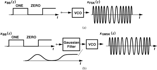
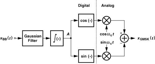
Called “Gaussian minimum shift keying” (GMSK), the scheme of Fig. 3.34(b) is used in GSM cell phones (Section 3.7). The GMSK waveform can be expressed as
![]()
where h(t) denotes the impulse response of the Gaussian filter. The modulation index, m, is a dimensionless quantity and has a value of 0.5. Owing to its constant envelope, GMSK allows optimization of PAs for high efficiency—with little attention to linearity.
A slightly different version of GMSK, called Gaussian frequency shift keying (GFSK), is employed in Bluetooth. The GFSK waveform is also given by Eq. (3.40) but with m = 0.3.
3.3.5 Quadrature Amplitude Modulation
Our study of PSK and QPSK has revealed a twofold reduction in the spectrum as a result of impressing the information on the quadrature components of the carrier. Can we extend this idea to further tighten the spectrum? A method that accomplishes this goal is called “quadrature amplitude modulation” (QAM).
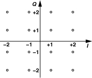
To arrive at QAM, let us first draw the four possible waveforms for QPSK corresponding to the four points in the constellation. As predicted by Eq. (3.31) and shown in Fig. 3.36(a), each quadrature component of the carrier is multipled by +1 or −1 according to the values of b2m and b2m+1. Now suppose we allow four possible amplitudes for the sine and cosine waveforms, e.g., ±1 and ±2, thus obtaining 16 possible output waveforms. Figure 3.36(b) depicts a few examples of such waveforms. In other words, we group four consecutive bits of the binary baseband stream and select one of the 16 waveforms accordingly. Called “16QAM,”6 the resulting output occupies one-fourth the bandwidth of PSK and is expressed as
![]()
Figure 3.36 Amplitude combinations in (a) QPSK and (b) 16QAM.

The constellation of 16QAM can be constructed using the 16 possible combinations of [α1 α2] (Fig. 3.37). For a given transmitted power [e.g., the rms value of the waveforms shown in Fig. 3.36(b)], the points in this constellation are closer to one another than those in the QPSK constellation, making the detection more sensitive to noise. This is the price paid for saving bandwidth.
Figure 3.37 Constellation of 16QAM signal.
In addition to a “dense” constellation, 16QAM also exhibits large envelope variations, as exemplified by the waveforms in Fig. 3.36. Thus, this type of modulation requires a highly-linear power amplifier. We again observe the trade-offs among bandwidth efficiency, detectability, and power efficiency.
The concept of QAM can be extended to even denser constellations. For example, if eight consecutive bits in the binary baseband stream are grouped and, accordingly, each quadrature component of the carrier is allowed to have eight possible amplitudes, then 64QAM is obtained. The bandwidth is therefore reduced by a factor of eight with respect to that of PSK, but the detection and power amplifier design become more difficult.
A number of applications employ QAM to save bandwidth. For example, IEEE802.11g/a uses 64QAM for the highest data rate (54 Mb/s).
3.3.6 Orthogonal Frequency Division Multiplexing
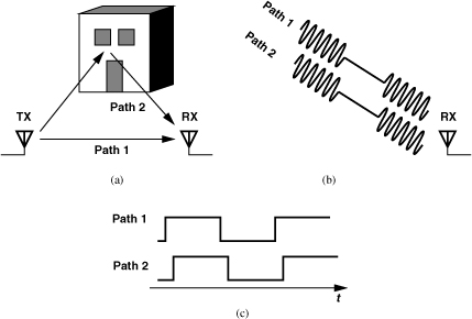
Communication in a wireless environment entails a serious issue called “multipath propagation.” Illustrated in Fig. 3.38(a), this effect arises from the propagation of the electromagnetic waves from the transmitter to the receiver through multiple paths. For example, one wave directly propagates from the TX to the RX while another is reflected from a wall before reaching the receiver. Since the phase shift associated with reflection(s) depends on both the path length and the reflecting material, the waves arrive at the RX with vastly different delays, or a large “delay spread.” Even if these delays do not result in destructive interference of the rays, they may lead to considerable intersymbol interference. To understand this point, suppose, for example, two ASK waveforms containing the same information reach the RX with different delays [Fig. 3.38(b)]. Since the antenna senses the sum of these waveforms, the baseband data consists of two copies of the signal that are shifted in time, thus experiencing ISI [Fig. 3.38(c)].
Figure 3.38 (a) Multipath propagation, (b) effect on received ASK waveforms, (c) baseband components exhibiting ISI due to delay spread.
The ISI resulting from multipath effects worsens for larger delay spreads or higher bit rates. For example, a data rate of 1 Mb/s becomes sensitive to multipath propagation if the delay spread reaches a fraction of a microsecond. As a rule of thumb, we say communication inside office buildings and homes begins to suffer from multipath effects for data rates greater than 10 Mb/s.
How does wireless communication handle higher data rates? An interesting method of delay spread mitigation is called “orthogonal frequency division multiplexing” (OFDM). Consider the “single-carrier” modulated spectrum shown in Fig. 3.39(a), which occupies a relatively large bandwidth due to a high data rate of rb bits per second. In OFDM, the baseband data is first demultiplexed by a factor of N, producing N streams each having a (symbol) rate of rb/N [Fig. 3.39(b)]. The N streams are then impressed on N different carrier frequencies, fc1-fcN, leading to a “multi-carrier” spectrum. Note that the total bandwidth and data rate remain equal to those of the single-carrier spectrum, but the multi-carrier signal is less sensitive to multipath effects because each carrier contains a low-rate data stream and can therefore tolerate a larger delay spread.
Figure 3.39 (a) Single-carrier modulator with high-rate input, (b) OFDM with multiple carriers.
Each of the N carriers in Fig. 3.39(b) is called a “subcarrier” and each resulting modulated output a “subchannel.” In practice, all of the subchannels utilize the same modulation scheme. For example, IEEE802.11a/g employs 48 subchannels with 64QAM in each for the highest data rate (54 Mb/s). Thus, each subchannel carries a symbol rate of (54 Mb/s)/48/8=141 ksymbol/s.
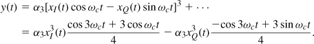
While providing greater immunity to multipath propagation, OFDM imposes severe linearity requirements on power amplifiers. This is because the N (orthogonal) subchannels summed at the output of the system in Fig. 3.39(b) may add constructively at some point in time, creating a large amplitude, and destructively at some other point in time, producing a small amplitude. That is, OFDM exhibits large envelope variations even if the modulated waveform in each subchannel does not.
In the design of power amplifiers, it is useful to have a quantitative measure of the signal’s envelope variations. One such measure is the “peak-to-average ratio” (PAR). As illustrated in Fig. 3.40, PAR is defined as the ratio of the largest value of the square of the signal (voltage or current) divided by the average value of the square of the signal:
![]()
Figure 3.40 Large amplitude variations due to OFDM.
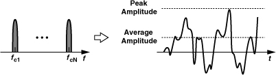
We note that three effects lead to a large PAR: pulse shaping in the baseband, amplitude modulation schemes such as QAM, and orthogonal frequency division multiplexing. For N subcarriers, the PAR of an OFDM waveform is about 2 ln N if N is large [6].
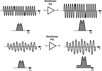
3.4 Spectral Regrowth
In our study of modulation schemes, we have mentioned that variable-envelope signals require linear PAs, whereas constant-envelope signals do not. Of course, modulation schemes such as 16QAM that carry information in their amplitude levels experience corruption if the PA compresses the larger levels, i.e., moves the outer points of the constellation toward the origin. But even variable-envelope signals that carry no significant information in their amplitude (e.g., QPSK with baseband pulse-shaping) create an undesirable effect in nonlinear PAs. Called “spectral regrowth,” this effect corrupts the adjacent channels.
A modulated waveform x(t) = A(t) cos[ωct + φ(t)] is said to have a constant envelope if A(t) does not vary with time. Otherwise, we say the signal has a variable envelope. Constant- and variable-envelope signals behave differently in a nonlinear system. Suppose A(t) = Ac and the system exhibits a third-order memoryless nonlinearity:

The first term in (3.46) represents a modulated signal around ω = 3ωc. Since the bandwidth of the original signal, Ac cos[ωct + φ(t)], is typically much less than ωc, the bandwidth occupied by cos[3ωct + 3φ(t)] is small enough that it does not reach the center frequency of ωc. Thus, the shape of the spectrum in the vicinity of ωc remains unchanged.
Now consider a variable-envelope signal applied to the above nonlinear system. Writing x(t) as
![]()
where xI and xQ(t) are the baseband I and Q components, we have
Thus, the output contains the spectra of ![]() and
and ![]() centered around ωc. Since these components generally exhibit a broader spectrum than do xI(t) and xQ(t), we say the spectrum “grows” when a variable-envelope signal passes through a nonlinear system. Figure 3.41 summarizes our findings.
centered around ωc. Since these components generally exhibit a broader spectrum than do xI(t) and xQ(t), we say the spectrum “grows” when a variable-envelope signal passes through a nonlinear system. Figure 3.41 summarizes our findings.
Figure 3.41 Amplification of constant- and variable-envelope signals and the effect on their spectra.
3.5 Mobile RF Communications
A mobile system is one in which users can physically move while communicating with one another. Examples include pagers, cellular phones, and cordless phones. It is the mobility that has made RF communications powerful and popular. The transceiver carried by the user is called the “mobile unit” (or simply the “mobile”), the “terminal,” or the “hand-held unit.” The complexity of the wireless infrastructure often demands that the mobiles communicate only through a fixed, relatively expensive unit called the “base station.” Each mobile receives and transmits information from and to the base station via two RF channels called the “forward channel” or “downlink” and the “reverse channel” or “uplink,” respectively. Most of our treatment in this book relates to the mobile unit because, compared to the base station, hand-held units constitute a much larger portion of the market and their design is much more similar to other types of RF systems.
Cellular System
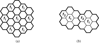
With the limited available spectrum (e.g., 25 MHz around 900 MHz), how do hundreds of thousands of people communicate in a crowded metropolitan area? To answer this question, we first consider a simpler case: thousands of FM radio broadcasting stations may operate in a country in the 88–108 MHz band. This is possible because stations that are physically far enough from each other can use the same carrier frequency (“frequency reuse”) with negligible mutual interference (except at some point in the middle where the stations are received with comparable signal levels). The minimum distance between two stations that can employ equal carrier frequencies depends on the signal power produced by each.
In mobile communications, the concept of frequency reuse is implemented in a “cellular” structure, where each cell is configured as a hexagon and surrounded by 6 other cells [Fig. 3.42(a)]. The idea is that if the center cell uses a frequency f1 for communication, the 6 neighboring cells cannot utilize this frequency, but the cells beyond the immediate neighbors may. In practice, more efficient frequency assignment leads to the “7-cell” reuse pattern shown in Fig. 3.42(b). Note that in reality each cell utilizes a group of frequencies.
Figure 3.42 (a) Simple cellular system, (b) 7-cell reuse pattern.
The mobile units in each cell of Fig. 3.42(b) are served by a base station, and all of the base stations are controlled by a “mobile telephone switching office” (MTSO).
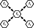
Co-Channel Interference
An important issue in a cellular system is how much two cells that use the same frequency interfere with each other (Fig. 3.43). Called “co-channel interference” (CCI), this effect depends on the ratio of the distance between two co-channel cells to the cell radius and is independent of the transmitted power. Given by the frequency reuse plan, this ratio is approximately equal to 4.6 for the 7-cell pattern of Fig. 3.42(b) [7]. It can be shown that this value yields a signal-to-co-channel interference ratio of 18 dB [7].
Figure 3.43 Co-channel interference.
Hand-off
What happens when a mobile unit “roams” from cell A to cell B (Fig. 3.44)? Since the power level received from the base station in cell A is insufficient to maintain communication, the mobile must change its server to the base station in cell B. Furthermore, since adjacent cells do not use the same group of frequencies, the channel must also change. Called “hand-off,” this process is performed by the MTSO. Once the level received by the base station in cell A drops below a threshold, the MTSO hands off the mobile to the base station in cell B, hoping that the latter is close enough. This strategy fails with relatively high probability, resulting in dropped calls.
Figure 3.44 Problem of hand-off.
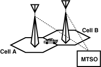
To improve the hand-off process, second-generation cellular systems allow the mobile unit to measure the received signal level from different base stations, thus performing hand-off when the path to the second base station has sufficiently low loss [7].
Path Loss and Multipath Fading
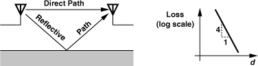
Propagation of signals in a mobile communication environment is quite complex. We briefly describe some of the important concepts here. Signals propagating through free space experience a power loss proportional to the square of the distance, d, from the source. In reality, however, the signal travels through both a direct path and an indirect, reflective path (Fig. 3.45). It can be shown that in this case, the loss increases with the fourth power of the distance [7]. In crowded areas, the actual loss profile may be proportional to d2 for some distance and d4 for another.
Figure 3.45 Indirect signal propagation and resulting loss profile.
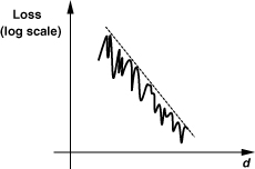
In addition to the overall loss profile depicted in Fig. 3.45, another mechanism gives rise to fluctuations in the received signal level as a function of distance. Since the two signals shown in Fig. 3.45 generally experience different phase shifts, possibly arriving at the receiver with opposite phases and roughly equal amplitudes, the net received signal may be very small. Called “multipath fading” and illustrated in Fig. 3.46, this phenomenon introduces enormous variations in the signal level as the receiver moves by a fraction of the wavelength. Note that multipath propagation creates fading and/or ISI.
Figure 3.46 Multipath loss profile.
In reality, since the transmitted signal is reflected by many buildings and moving cars, the fluctuations are quite irregular. Nonetheless, the overall received signal can be expressed as
For large n, each summation has a Gaussian distribution. Denoting the first summation by A and the second by B, we have
![]()
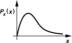
where φ = tan−1(B/A). It can be shown that the amplitude, ![]() , has a Rayleigh distribution (Fig. 3.47) [1], exhibiting losses greater than 10 dB below the mean for approximately 6% of the time.
, has a Rayleigh distribution (Fig. 3.47) [1], exhibiting losses greater than 10 dB below the mean for approximately 6% of the time.
Figure 3.47 Rayleigh distribution.
From the above discussion, we conclude that in an RF system the transmitter output power and the receiver dynamic range must be chosen so as to accommodate signal level variations due to both the overall path loss (roughly proportional to d4) and the deep multipath fading effects. While it is theoretically possible that multipath fading yields a zero amplitude (infinite loss) at a given distance, the probability of this event is negligible because moving objects in a mobile environment tend to “soften” the fading.
Diversity
The effect of fading can be lowered by adding redundancy to the transmission or reception of the signal. “Space diversity” or “antenna diversity” employs two or more antennas spaced apart by a significant fraction of the wavelength so as to achieve a higher probability of receiving a nonfaded signal.
“Frequency diversity” refers to the case where multiple carrier frequencies are used, with the idea that fading is unlikely to occur simultaneously at two frequencies sufficiently far from each other. “Time diversity” is another technique whereby the data is transmitted or received more than once to overcome short-term fading.
Delay Spread
Suppose two signals in a multipath environment experience roughly equal attenuations but different delays. This is possible because the absorption coefficient and phase shift of reflective or refractive materials vary widely, making it likely for two paths to exhibit equal loss and unequal delays. Addition of two such signals yields x(t) = A cos ω(t−τ1) + A cos ω(t−τ2) = 2A cos[(2ωt−ωτ1 −ωτ2)/2] cos[ω(τ1 − τ2)/2], where the second cosine factor relates the fading to the “delay spread,” Δτ = τ1 − τ2. An important issue here is the frequency dependence of the fade. As illustrated in Fig. 3.48, small delay spreads yield a relatively flat fade, whereas large delay spreads introduce considerable variation in the spectrum.
Figure 3.48 (a) Flat and (b) frequency-selective fading.

In a multipath environment, many signals arrive at the receiver with different delays, yielding rms delay spreads as large as several microseconds and hence fading bandwidths of several hundreds of kilohertz. Thus, an entire communication channel may be suppressed during such a fade.
Interleaving
The nature of multipath fading and the signal processing techniques used to alleviate this issue is such that errors occur in clusters of bits. In order to lower the effect of these errors, the baseband bit stream in the transmitter undergoes “interleaving” before modulation. An interleaver in essence scrambles the time order of the bits according to an algorithm known by the receiver [7].
3.6 Multiple Access Techniques
3.6.1 Time and Frequency Division Duplexing
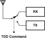
The simplest case of multiple access is the problem of two-way communication by a transceiver, a function called “duplexing.” In old walkie-talkies, for example, the user would press the “talk” button to transmit while disabling the receive path and release the button to listen while disabling the transmit path. This can be considered a simple form of “time division duplexing,” (TDD), whereby the same frequency band is utilized for both transmit (TX) and receive (RX) paths but the system transmits for half of the time and receives for the other half. Illustrated in Fig. 3.49, TDD is usually performed fast enough to be transparent to the user.
Figure 3.49 Time-division duplexing.
Another approach to duplexing is to employ two different frequency bands for the transmit and receive paths. Called “frequency-division duplexing” (FDD) and shown in Fig. 3.50, this technique incorporates band-pass filters to isolate the two paths, allowing simultaneous transmission and reception. Since two such transceivers cannot communicate directly, the TX band must be translated to the RX band at some point. In wireless networks, this translation is performed in the base station.
Figure 3.50 Frequency-division duplexing.

It is instructive to contrast the two duplexing methods by considering their merits and drawbacks. In TDD, an RF switch with a loss less than 1 dB follows the antenna to alternately enable and disable the TX and RX paths. Even though the transmitter output power may be 100 dB above the receiver input signal, the two paths do not interfere because the transmitter is turned off during reception. Furthermore, TDD allows direct (“peer-to-peer”) communication between two transceivers, an especially useful feature in short-range, local area network applications. The primary drawback of TDD is that the strong signals generated by all of the nearby mobile transmitters fall in the receive band, thus desensitizing the receiver.
In FDD systems, the two front-end band-pass filters are combined to form a “duplexer filter.” While making the receivers immune to the strong signals transmitted by other mobile units, FDD suffers from a number of issues. First, components of the transmitted signal that leak into the receive band are attenuated by typically only about 50 dB (Chapter 4). Second, owing to the trade-off between the loss and the quality factor of filters, the loss of the duplexer is typically quite higher than that of a TDD switch. Note that a loss of, say, 3 dB in the RX path of the duplexer raises the overall noise figure by 3 dB (Chapter 2), and the same loss in the TX path of the filter means that only 50% of the signal power reaches the antenna.
Another issue in FDD is the spectral leakage to adjacent channels in the transmitter output. This occurs when the power amplifier is turned on and off to save energy or when the local oscillator driving the modulator undergoes a transient. By contrast, in TDD such transients can be timed to end before the antenna is switched to the power amplifier output.
Despite the above drawbacks, FDD is employed in many RF systems, particularly in cellular communications, because it isolates the receivers from the signals produced by mobile transmitters.
3.6.2 Frequency-Division Multiple Access
In order to allow simultaneous communication among multiple transceivers, the available frequency band can be partitioned into many channels, each of which is assigned to one user. Called “frequency-division multiple access,” (Fig. 3.51), this technique should be familiar within the context of radio and television broadcasting, where the channel assignment does not change with time. In multiple-user, two-way communications, on the other hand, the channel assignment may remain fixed only until the end of the call; after the user hangs up the phone, the channel becomes available to others. Note that in FDMA with FDD, two channels are assigned to each user, one for transmit and another for receive.
Figure 3.51 Frequency-division multiple access.

The relative simplicity of FDMA made it the principal access method in early cellular networks, called “analog FM” systems. However, in FDMA the minimum number of simultaneous users is given by the ratio of the total available frequency band (e.g., 25 MHz in GSM) and the width of each channel (e.g., 200 kHz in GSM), translating to insufficient capacity in crowded areas.
3.6.3 Time-Division Multiple Access
In another implementation of multiple-access networks, the same band is available to each user but at different times (“time-division multiple access”). Illustrated in Fig. 3.52, TDMA periodically enables each of the transceivers for a “time slot” (Tsl). The overall period consisting of all of the time slots is called a “frame” (TF). In other words, every TF seconds, each user finds access to the channel for Tsl seconds.
Figure 3.52 Time-division multiple access.

What happens to the data (e.g., voice) produced by all other users while only one user is allowed to transmit? To avoid loss of information, the data is stored (“buffered”) for TF − Tsl seconds and transmitted as a burst during one time slot (hence the term “TDMA burst”). Since buffering requires the data to be in digital form, TDMA transmitters perform A/D conversion on the analog input signal. Digitization also allows speech compression and coding.
TDMA systems have a number of advantages over their FDMA counterparts. First, as each transmitter is enabled for only one time slot in every frame, the power amplifier can be turned off during the rest of the frame, thus saving considerable power. In practice, settling issues require that the PA be turned on slightly before the actual time slot begins. Second, since digitized speech can be compressed in time by a large factor, the required communication bandwidth can be smaller and hence the overall capacity larger. Equivalently, as compressed speech can be transmitted over a shorter time slot, a higher number of users can be accommodated in each frame. Third, even with FDD, the TDMA bursts can be timed such that the receive and transmit paths in each transceiver are never enabled simultaneously.
The need for A/D conversion, digital modulation, time slot and frame synchronization, etc., makes TDMA more complex than FDMA. With the advent of VLSI DSPs, however, this drawback is no longer a determining factor. In most actual TDMA systems, a combination of TDMA and FDMA is utilized. In other words, each of the channels depicted in Fig. 3.51 is time-shared among many users.
3.6.4 Code-Division Multiple Access
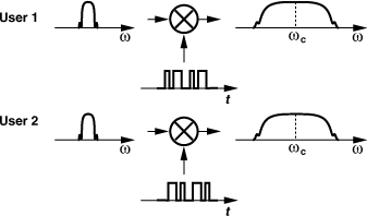
Our discussion of FDMA and TDMA implies that the transmitted signals in these systems avoid interfering with each other in either the frequency domain or the time domain. In essence, the signals are orthogonal in one of these domains. A third method of multiple access allows complete overlap of signals in both frequency and time, but employs “orthogonal messages” to avoid interference. This can be understood with the aid of an analogy [8]. Suppose many conversations are going on in a crowded party. To minimize crosstalk, different groups of people can be required to speak in different pitches(!) (FDMA), or only one group can be allowed to converse at a time (TDMA). Alternatively, each group can be asked to speak in a different language. If the languages are orthogonal (at least in nearby groups) and the voice levels are roughly the same, then each listener can “tune in” to the proper language and receive information while all groups talk simultaneously.
Direct-Sequence CDMA
In “code-division multiple access,” different languages are created by means of orthogonal digital codes. At the beginning of communication, a certain code is assigned to each transmitter-receiver pair, and each bit of the baseband data is “translated” to that code before modulation. Shown in Fig. 3.53(a) is an example where each baseband pulse is replaced with an 8-bit code by multiplication. A method of generating orthogonal codes is based on Walsh’s recursive equation:
![]()
![]()
where ![]() is derived from Wn by replacing all the entries with their complements. For example,
is derived from Wn by replacing all the entries with their complements. For example,
![]()
Figure 3.53 (a) Encoding operation in DS-CDMA, (b) examples of Walsh code.
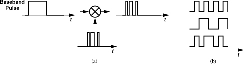
Fig. 3.53(b) shows examples of 8-bit Walsh codes (i.e., each row of W8).
In the receiver, the demodulated signal is decoded by multiplying it by the same Walsh code. In other words, the receiver correlates the signal with the code to recover the baseband data.
How is the received data affected when another CDMA signal is present? Suppose two CDMA signals x1(t) and x2(t) are received in the same frequency band. Writing the signals as xBB1(t) · W1(t) and xBB2(t) · W2(t), where W1(t) and W2(t) are Walsh functions, we express the output of the demodulator as y(t) = [xBB1(t). W1(t) + xBB2(t). W2(t)]. W1(t). Thus, if W1(t) and W2(t) are exactly orthogonal, then y(t) = xBB1(t) · W1(t). In reality, however, x1(t) and x2(t) may experience different delays, leading to corruption of y(t) by xBB2(t). Nevertheless, for long codes the result appears as random noise.
The encoding operation of Fig. 3.53(a) increases the bandwidth of the data spectrum by the number of pulses in the code. This may appear in contradiction to our emphasis thus far on spectral efficiency. However, since CDMA allows the widened spectra of many users to fall in the same frequency band (Fig. 3.54), this access technique has no less capacity than do FDMA and TDMA. In fact, CDMA can potentially achieve a higher capacity than the other two [9].
Figure 3.54 Overlapping spectra in CDMA.
CDMA is a special case of “spread spectrum” (SS) communications, whereby the baseband data of each user is spread over the entire available bandwidth. In this context, CDMA is also called “direct sequence” SS (DS-SS) communication, and the code is called the “spreading sequence” or “pseudo-random noise.” To avoid confusion with the baseband data, each pulse in the spreading sequence is called a “chip” and the rate of the sequence is called the “chip rate.” Thus, the spectrum is spread by the ratio of the chip rate to the baseband bit rate.
It is instructive to reexamine the above RX decoding operation from a spread spectrum point of view (Fig. 3.55). Upon multiplication by W1(t), the desired signal is “despread,” with its bandwidth returning to the original value. The unwanted signal, on the other hand, remains spread even after multiplication because of its low correlation with W1(t). For a large number of users, the spread spectra of unwanted signals can be viewed as white Gaussian noise.
Figure 3.55 Despreading operation in a CDMA receiver.

An important feature of CDMA is its soft capacity limit [7]. While in FDMA and TDMA the maximum number of users is fixed once the channel width or the time slots are defined, in CDMA increasing the number of users only gradually (linearly) raises the noise floor [7].
A critical issue in DS-CDMA is power control. Suppose, as illustrated in Fig. 3.56, the desired signal power received at a point is much lower than that of an unwanted transmitter,7 for example because the latter is at a shorter distance. Even after despreading, the strong interferer greatly raises the noise floor, degrading the reception of the desired signal. For multiple users, this means that one high-power transmitter can virtually halt communications among others, a problem much less serious in FDMA and TDMA. This is called the “near/far effect.” For this reason, when many CDMA transmitters communicate with a receiver, they must adjust their output power such that the receiver senses roughly equal signal levels. To this end, the receiver monitors the signal strength corresponding to each transmitter and periodically sends a power adjustment request to each one. Since in a cellular system users communicate through the base station, rather than directly, the latter must handle the task of power control. The received signal levels are controlled to be typically within 1 dB of each other.
Figure 3.56 Near/far effect in CDMA.

While adding complexity to the system, power control generally reduces the average power dissipation of the mobile unit. To understand this, note that without such control, the mobile must always transmit enough power to be able to communicate with the base station, whether path loss and fading are significant or not. Thus, even when the channel has minimum attenuation, the mobile unit produces the maximum output power. With power control, on the other hand, the mobile can transmit at low levels whenever the channel conditions improve. This also reduces the average interference seen by other users.
Unfortunately, power control also dictates that the receive and transmit paths of the mobile phone operate concurrently.8 As a consequence, CDMA mobile phones must deal with the leakage of the TX signal to the RX (Chapter 4).
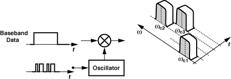
Frequency-Hopping CDMA
Another type of CDMA that has begun to appear in RF communications is “frequency hopping” (FH). Illustrated in Fig. 3.57, this access technique can be viewed as FDMA with pseudo-random channel allocation. The carrier frequency in each transmitter is “hopped” according to a chosen code (similar to the spreading codes in DS-CDMA). Thus, even though the short-term spectrum of a transmitter may overlap with those of others, the overall trajectory of the spectrum, i.e., the PN code, distinguishes each transmitter from others. Nevertheless, occasional overlap of the spectra raises the probability of error.
Figure 3.57 Frequency-hopping CDMA.
Due to rare overlap of spectra, frequency hopping is somewhat similar to FDMA and hence more tolerant of different received power levels than is direct-sequence CMDA. However, FH may require relatively fast settling in the control loop of the oscillator shown in Fig. 3.57, an important design issue studied in Chapter 10.
3.7 Wireless Standards
Our study of wireless communication systems thus far indicates that making a phone call or sending data entails a great many complex operations in both analog and digital domains. Furthermore, nonidealities such as noise and interference require precise specification of each system parameter, e.g., SNR, BER, occupied bandwidth, and tolerance of interferers. A “wireless standard” defines the essential functions and specifications that govern the design of the transceiver, including its baseband processing. Anticipating various operating conditions, each standard fills a relatively large document while still leaving some of the dependent specifications for the designer to choose. For example, a standard may specify the sensitivity but not the noise figure.
Before studying various wireless standards, we briefly consider some of the common specifications that standards quantify:
1. Frequency Bands and Channelization. Each standard performs communication in an allocated frequency band. For example, Bluetooth uses the industrial-scientific-medical (ISM) band from 2.400 GHz to 2.480 GHz. The band consists of “channels,” each of which carries the information for one user. For example, Bluetooth incorporates a channel of 1 MHz, allowing at most 80 users.
2. Data Rate(s). The standard specifies the data rate(s) that must be supported. Some standards support a constant data rate, whereas others allow a variable data rate so that, in the presence of high signal attenuation, the communication is sustained but at a low speed. For example, Bluetooth specifies a data rate of 1 Mb/s.
3. Antenna Duplexing Method. Most cellular phone systems incorporate FDD, and other standards employ TDD.
4. Type of Modulation. Each standard specifies the modulation scheme. In some cases, different modulation schemes are used for different data rates. For example, IEEE802.11a/g utilizes 64QAM for its highest rate (54 Mb/s) in the presence of good signal conditions, but binary PSK for the lowest rate (6 Mb/s).
5. TX Output Power. The standard specifies the power level(s) that the TX must produce. For example, Bluetooth transmits 0 dBm. Some standards require a variable output level to save battery power when the TX and RX are close to each other and/or to avoid near/far effects.
6. TX EVM and Spectral Mask. The signal transmitted by the TX must satisfy several requirements in addition to the power level. First, to ensure acceptable signal quality, the EVM is specified. Second, to guarantee that the TX out-of-channel emissions remain sufficiently small, a TX “spectral mask” is defined. As explained in Section 3.4, excessive PA nonlinearity may violate this mask. Also, the standard poses a limit on other unwanted transmitted components, e.g., spurs and harmonics.
7. RX Sensitivity. The standard specifies the acceptable receiver sensitivity, usually in terms of a maximum bit error rate, BERmax. In some cases, the sensitivity is commensurate with the data rate, i.e., a higher sensitivity is stipulated for lower data rates.
8. RX Input Level Range. The desired signal sensed by a receiver may range from the sensitivity level to a much larger value if the RX is close to the TX. Thus, the standard specifies the desired signal range that the receiver must handle with acceptable noise or distortion.
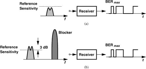
9. RX Tolerance to Blockers. The standard specifies the largest interferer that the RX must tolerate while receiving a small desired signal. This performance is typically defined as illustrated in Fig. 3.58. In the first step, a modulated signal is applied at the “reference” sensitivity level and the BER is measured to remain below BERmax [Fig. 3.58(a)]. In the second step, the signal level is raised by 3 dB and a blocker is added to the input and its level is gradually raised. When the blocker reaches the specified level, the BER must not exceed BERmax [Fig. 3.58(b)]. This test reveals the compression behavior and phase noise of the receiver. The latter is described in Chapter 8.
Figure 3.58 Test of a receiver with (a) desired signal at reference sensitivity and (b) desired signal 3 dB above reference sensitivity along with a blocker.
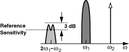
Many standards also stipulate an intermodulation test. For example, as shown in Fig. 3.59, two blockers (one modulated and another not) are applied along with the desired signal at 3 dB above the sensitivity level. The receiver BER must not exceed BERmax as the level of the two blockers reaches the specified level.
Figure 3.59 Intermodulation test.
In this section, we study a number of wireless standards. In the case of cellular standards, we focus on the “mobile station” (the handset).
3.7.1 GSM
The Global System for Mobile Communication (GSM) was originally developed as a unified wireless standard for Europe and became the most widely-used cellular standard in the world. In addition to voice, GSM also supports the transmission of data.
The GSM standard is a TDMA/FDD system with GMSK modulation, operating in different bands and accordingly called GSM900, GSM1800 (also known as DCS1800), and GSM1900 (also known as PCS1900). Figure 3.60 shows the TX and RX bands. Accommodating eight time-multiplexed users, each channel is 200 kHz wide, and the data rate per user is 271 kb/s. The TX and RX time slots are offset (by about 1.73 ms) so that the two paths do not operate simultaneously. The total capacity of the system is given by the number of channels in the 25-MHz bandwidth and the number of users is per channel, amounting to approximately 1,000.
Figure 3.60 GSM air interface.

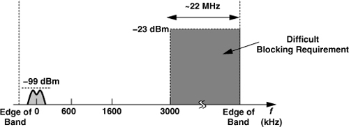
Blocking Requirements
GSM also specifies blocking requirements for the receiver. Illustrated in Fig. 3.61, the blocking test applies the desired signal at 3 dB above the sensitivity level along with a single (unmodulated) tone at discrete increments of 200 kHz from the desired channel. (Only one blocker is applied at a time.)10 The tolerable in-band blocker level jumps to −33 dBm at 1.6 MHz from the desired channel and to −23 dBm at 3 MHz. The out-of-band blocker can reach 0 dBm beyond a 20-MHz guard band from the edge of the RX band. With the blocker levels shown in Fig. 3.61, the receiver must still provide the necessary BER.
Figure 3.61 GSM receiver blocking test. (The desired channel center frequency is denoted by 0 for simplicity.)

If the receiver P1dB is determined by the blocker levels beyond 3-MHz offset, why does GSM specify the levels at smaller offsets? Another receiver imperfection, namely, the phase noise of the oscillator, manifests itself here and is discussed in Chapter 8.
Since the blocking requirements of Fig. 3.61 prove difficult to fulfill in practice, GSM stipulates a set of “spurious response exceptions,” allowing the blocker level at six in-band frequencies and 24 out-of-band frequencies to be relaxed to −43 dBm.11 Unfortunately, these exceptions do not ease the compression and phase noise requirements. For example, if the desired channel is near one edge of the band (Fig. 3.62), then about 100 channels reside above 3-MHz offset. Even if six of these channels are excepted, each of the remaining can contain a −23 dBm blocker.
Figure 3.62 Worst-case channel for GSM blocking test.
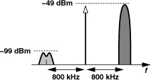
Intermodulation Requirements
Figure 3.63 depicts the IM test specified by GSM. With the desired channel 3 dB above the reference sensitivity level, a tone and a modulated signal are applied at 800-kHz and 1.6-MHz offset, respectively. The receiver must satisfy the required BER if the level of the two interferers is as high as −49 dBm.
Figure 3.63 GSM intermodulation test.
Adjacent-Channel Interference
A GSM receiver must withstand an adjacent-channel interferer 9 dB above the desired signal or an alternate-adjacent channel interferer 41 dB above the desired signal (Fig. 3.64). In this test, the desired signal is 20 dB higher than the sensitivity level. As explained in Chapter 4, the relatively relaxed adjacent-channel requirement facilitates the use of certain receiver architectures.
Figure 3.64 GSM adjacent-channel test.

TX Specifications
A GSM (mobile) transmitter must deliver an output power of at least 2 W (+33 dBm) in the 900-MHz band or 1 W in the 1.8-GHz band. Moreover, the output power must be adjustable in steps of 2 dB from +5 dBm to the maximum level, allowing adaptive power control as the mobile comes closer to or goes farther from the base station.
The output spectrum produced by a GSM transmitter must satisfy the “mask” shown in Fig. 3.65, dictating that GMSK modulation be realized with an accurate modulation index and well-controlled pulse shaping. Also, the rms phase error of the output signal must remain below 5°.
Figure 3.65 GSM transmission mask for the 900-MHz band.

A stringent specification in GSM relates to the maximum noise that the TX can emit in the receive band. As shown in Fig. 3.66, this noise level must be less than −129 dBm/Hz so that a transmitting mobile station negligibly interferes with a receiving mobile station in its close proximity. The severity of this requirement becomes obvious if the noise bound is normalized to the TX output power of +33 dBm, yielding a relative noise floor of −162 dBc/Hz. As explained in Chapter 4, this specification makes the design of GSM transmitters quite difficult.
Figure 3.66 GSM transmitter noise in receive band.

EDGE
To accommodate higher data rates in a 200-kHz channel, the GSM standard has been extended to “Enhanced Data Rates for GSM Evolution” (EDGE). Achieving a rate of 384 kb/s, EDGE employs “8-PSK” modulation, i.e., phase modulation with eight phase values given by kπ/4, k = 0-7. Figure 3.67 shows the signal constellation. EDGE is considered a “2.5th-generation” (2.5G) cellular system.
The use of 8-PSK modulation entails two issues. First, to confine the spectrum to 200 kHz, a “linear” modulation with baseband pulse shaping is necessary. In fact, the constellation of Fig. 3.67 can be viewed as that of two QPSK waveforms, one rotated by 45° with respect to the other. Thus, two QPSK signals with pulse shaping (Chapter 4) can be generated and combined to yield the 8-PSK waveform. Pulse shaping, however, leads to a variable envelope, necessitating a linear power amplifier. In other words, a GSM/EDGE transmitter can operate with a nonlinear (and hence efficient) PA in the GSM mode but must switch to a linear (and hence inefficient) PA in the EDGE mode.
Figure 3.67 Constellation of 8-PSK (used in EDGE).
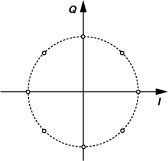
The second issue concerns the detection of the 8-PSK signal in the receiver. The closely-spaced points in the constellation require a higher SNR than, say, QPSK does. For BER = 10−3, the former dictates an SNR of 14 dB and the latter, 7 dB.
3.7.2 IS-95 CDMA
A wireless standard based on direct-sequence CMDA has been proposed by Qualcomm, Inc., and adopted for North America as IS-95. Using FDD, the air interface employs the transmit and receive bands shown in Fig. 3.68. In the mobile unit, the 9.6 kb/s baseband data is spread to 1.23 MHz and subsequently modulated using OQPSK. The link from the base station to the mobile unit, on the other hand, incorporates QPSK modulation. The logic is that the mobile must use a power-efficient modulation scheme (Chapter 3), whereas the base station transmits many channels simultaneously and must therefore employ a linear power amplifier regardless of the type of modulation. In both directions, IS-95 requires coherent detection, a task accomplished by transmitting a relatively strong “pilot tone” (e.g., unmodulated carrier) at the beginning of communication to establish phase synchronization.
Figure 3.68 IS-95 air interface.

In contrast to the other standards studied above, IS-95 is substantially more complex, incorporating many techniques to increase the capacity while maintaining a reasonable signal quality. We briefly describe some of the features here. For more details, the reader is referred to [8, 10, 11].
Power Control
As mentioned in Section 3.6.4, in CDMA the power levels received by the base station from various mobile units must differ by no more than approximately 1 dB. In IS-95, the output power of each mobile is controlled by an open-loop procedure at the beginning of communication so as to perform a rough but fast adjustment. Subsequently, the power is set more accurately by a closed-loop method. For open-loop control, the mobile measures the signal power it receives from the base station and adjusts its transmitted power so that the sum of the two (in dB) is approximately −73 dBm. If the receive and transmit paths entail roughly equal attenuation, k dB, and the power transmitted by the base station is Pbs, then the mobile output power Pm satisfies the following: Pbs − k + Pm = −73 dBm. Since the power received by the base station is Pm − k, we have Pm − k = −73 dBm −Pbs, a well-defined value because Pbs is usually fixed. The mobile output power can be varied by approximately 85 dB in a few microseconds.
Closed-loop power control is also necessary because the above assumption of equal loss in the transmit and receive paths is merely an approximation. In reality, the two paths may experience different fading because they operate in different frequency bands. To this end, the base station measures the power level received from the mobile unit and sends a feedback signal requesting power adjustment. This command is transmitted once every 1.25 ms to ensure timely adjustment in the presence of rapid fading.
Frequency and Time Diversity
Recall from Section 3.5 that multipath fading is often frequency-selective, causing a notch in the channel transfer function that can be several kilohertz wide. Since IS-95 spreads the spectrum to 1.23 MHz, it provides frequency diversity, exhibiting only 25% loss of the band for typical delay spreads [8].
IS-95 also employs time diversity to use multipath signals to advantage. This is accomplished by performing correlation on delayed replicas of the received signal (Fig. 3.69). Called a “rake receiver,” such a system combines the delayed replicas with proper weighting factors, αj, to obtain the maximum signal-to-noise ratio at the output. That is, if the output of one correlator is corrupted, then the corresponding weighting factor is reduced and vice versa.
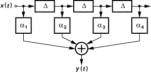
Rake receivers are a unique feature of CDMA. Since the chip rate is much higher than the fading bandwidth, and since the spreading codes are designed to have negligible correlation for delays greater than a chip period, multipath effects do not introduce intersymbol interference. Thus, each correlator can be synchronized to one of the multipath signals.
Variable Coding Rate
The variable rate of information in human speech can be exploited to lower the average number of transmitted bits per second. In IS-95, the data rate can vary in four discrete steps: 9600, 4800, 2400, and 1200 b/s. This arrangement allows buffering slower data such that the transmission still occurs at 9600 b/s but for a proportionally shorter duration. This approach further reduces the average power transmitted by the mobile unit, both saving battery and lowering interference seen by other users.
Soft Hand-off
Recall from Section 3.5 that when the mobile unit is assigned a different base station, the call may be dropped if the channel center frequency must change (e.g., in IS-54 and GSM). In CDMA, on the other hand, all of the users in one cell communicate on the same channel. Thus, as the mobile unit moves farther from one base station and closer to another, the signal strength corresponding to both stations can be monitored by means of a rake receiver. When it is ascertained that the nearer base station has a sufficiently strong signal, the hand-off is performed. Called “soft hand-off,” this method can be viewed as a “make-before-break” operation. The result is lower probability of dropping calls during hand-off.
3.7.3 Wideband CDMA
As a third-generation cellular system, wideband CDMA extends the concepts realized in IS-95 to achieve a higher data rate. Using BPSK (for uplink) and QPSK (for downlink) in a nominal channel bandwidth of 5 MHz, WCDMA achieves a rate of 384 kb/s.
Several variants of WCDMA have been deployed in different graphical regions. In this section, we study “IMT-2000” as an example. Figure 3.70 shows the air interface of IMT-2000, indicating a total bandwidth of 60 MHz. Each channel can accommodate a data rate of 384 kb/s in a (spread) bandwidth of 3.84 MHz; but, with “guard bands” included, the channel spacing is 5 MHz. The mobile station employs BPSK modulation for data and QPSK modulation for spreading.
Figure 3.70 IMT-2000 air interface.

Transmitter Requirements
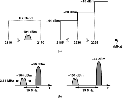
The TX must deliver an output power ranging from −49 dBm to +24 dBm.12 The wide output dynamic range makes the design of WCDMA transmitters and, specifically, power amplifiers, difficult. In addition, the TX incorporates baseband pulse shaping so as to tighten the output spectrum, calling for a linear PA. IMT-2000 stipulates two sets of specifications to quantify the limits on the out-of-channel emissions: (1) the adjacent and alternate adjacent channel powers must be 33 dB and 43 dB below the main channel, respectively [Fig. 3.71(a)]; (2) the emissions measured in a 30-kHz bandwidth must satisfy the TX mask shown in Fig. 3.71(b).
Figure 3.71 Transmitter (a) adjacent-channel power test, and (b) emission mask in IMT-2000.

The transmitter must also coexist harmoniously with the GSM and DCS1800 standards. That is, the TX power must remain below −79 dBm in a 100-kHz bandwidth in the GSM RX band (935 MHz-960 MHz) and below −71 dBm in a 100-kHz bandwidth in the DCS1800 RX band (1805 MHz-1880 MHz).
Receiver Requirements
The receiver reference sensitivity is −107 dBm. As with GSM, IMT-2000 receivers must withstand a sinusoidal blocker whose amplitude becomes larger at greater frequency offsets. Unlike GSM, however, IMT-2000 requires the sinusoidal test for only out-of-band blocking [Fig. 3.72(a)]. The P1dB necessary here is more relaxed than that in GSM; e.g., at 85 MHz outside the band, the RX must tolerate a tone of −15 dBm.13 For in-band blocking, IMT-2000 provides the two tests shown in Fig. 3.72(b). Here, the blocker is modulated such that it behaves as another WCDMA channel, thus causing both compression and cross modulation.
Figure 3.72 IMT-2000 receiver (a) blocking mask using a tone and (b) blocking test using a modulated interferer.
Solution:
![]()
For the case at hand, both channels contain modulation and we make the following assumptions: (1) the desired channel and the blocker carry the same amplitude modulation and are respectively expressed as A1(1 + m cos ωm1t) cos ω1t and A2(1 + m cos ωm2t) cos ω2t; (2) the envelope varies by a moderate amount and hence m2/2 ![]() 2m. The effect of third-order nonlinearity can then be expressed as
2m. The effect of third-order nonlinearity can then be expressed as
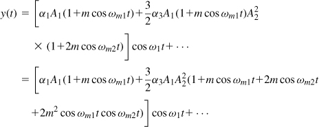

Since ![]() and hence
and hence ![]() ,
,
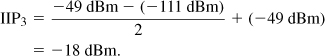
![]()
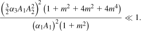
A sensitivity level of −107 dBm with a signal bandwidth as wide as 3.84 MHz may appear very impressive. In fact, since 10 log(3.84 MHz) ≈ 66 dB, it seems that the sum of the receiver noise figure and the required SNR must not exceed 174 dBm/Hz − 66 dB − 107 dBm = 1 dB! However, recall that CDMA spreads a lower bit rate (e.g., 384 kb/s) by a factor, thus benefitting from the spreading gain after the despreading operation in the receiver. That is, the NF is relaxed by a factor equal to the spreading gain.
IMT-2000 also specifies an intermodulation test. As depicted in Fig. 3.73, a tone and a modulated signal, each at −46 dBm, are applied in the adjacent and alternate adjacent channels, respectively, while the desired signal is at −104 dBm. In Problem 3.3, we repeat Example 3.12 for WCDMA to determine the required IP3 of the receiver.
Figure 3.73 IMT-2000 intermodulation test.
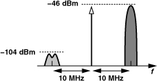
Figure 3.74 illustrates the adjacent-channel test stipulated by IMT-2000. With a level of −93 dBm for the desired signal, the adjacent channel can be as high as −52 dBm. As explained in Chapter 4, this specification requires a sharp roll-off in the frequency response of the baseband filters.
Figure 3.74 IMT-2000 receiver adjacent-channel test.

3.7.4 Bluetooth
The Bluetooth standard was originally conceived as a low-cost solution for short-range, moderate-rate data communication. In fact, it was envisioned that the transceiver would perform modulation and demodulation in the analog domain, requiring little digital signal processing. In practice, however, some attributes of the standard have made the analog implementations difficult, calling for substantial processing in the digital domain. Despite these challenges, Bluetooth has found its place in the consumer market, serving in such short-reach applications as wireless headsets, wireless keyboards, etc.
Figure 3.75 shows the Bluetooth air interface, indicating operation in the 2.4-GHz ISM band. Each channel carries 1 Mb/s, occupies 1 MHz, and has a carrier frequency equal to (2402 + k) MHz, for k = 0, ..., 78. To comply with out-of-band emission requirements of various countries, the first 2 MHz and last 3.5 MHz of the ISM band are saved as “guard bands” and not used.
Figure 3.75 Bluetooth air interface.

Transmitter Characteristics
The 1-Mb/s baseband data is applied to a Gaussian Frequency Shift Keying (GFSK) modulator. GFSK can be viewed as GMSK with a modulation index of 0.28 to 0.35. As explained in Section 3.3.4, GMSK modulation can be realized by a Gaussian filter and a VCO (Fig. 3.76).
Figure 3.76 GFSK modulation using a VCO.
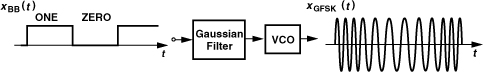
The output can be expressed as
![]()
where h(t) denotes the impulse response of the Gaussian filter. As shown in Fig. 3.77, Bluetooth specifies a minimum frequency deviation of 115 kHz in the carrier. The peak frequency deviation, Δf, is obtained as the maximum difference between the instantaneous frequency, finst, and the carrier frequency. Differentiating the argument of the cosine in (3.66) yields finst as
![]()
suggesting that
![]()
Figure 3.77 Frequency deviation in Bluetooth.
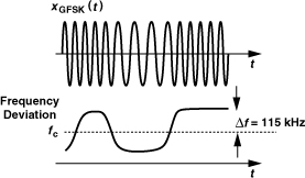
Since the peak voltage swing at the output of the Gaussian filter is approximately equal to that of xBB(t),
![]()
As explained in Chapter 8, m is a property of the voltage-controlled oscillator (called the “gain” of the VCO) and must be chosen to satisfy (3.69).
Bluetooth specifies an output level of 0 dBm (1 mW).14 Along with the constant-envelope modulation, this relaxed value greatly simplifies the design of the power amplifier, allowing it to be a simple 50-Ω buffer.
The Bluetooth transmit spectrum mask is shown in Fig. 3.78. At an offset of 550 kHz from the center of the desired channel, the power measured in a 100-kHz bandwidth must be at least 20 dB below the TX power measured in the same bandwidth but in the center of the channel. Moreover, the power measured in the entire 1-MHz alternate adjacent channel must remain below −20 dBm. Similarly, the power in the third and higher adjacent channels must be less than −40 dBm.15
Figure 3.78 Bluetooth transmission mask.
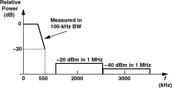
A Bluetooth TX must minimally interfere with cellular and WLAN systems. For example, it must produce in a 100-kHz bandwidth less than −47 dBm in the range of 1.8 GHz to 1.9 GHz or 5.15 GHz to 5.3 GHz.
The carrier frequency of each Bluetooth carrier has a tolerance of ±75 kHz (≈ ±30 ppm). Since the carrier synthesis is based on a reference crystal frequency (Chapter 10), the crystal must have an error of less than ±30 ppm.
Receiver Characteristics
Bluetooth operates with a reference sensitivity of −70 dBm (for BER=10−3), but most commercial products push this value to about −80 dBm, affording longer range.
Figure 3.79 illustrates the blocking tests specified by Bluetooth. In Fig. 3.79(a), the desired signal is 10 dB higher than the reference sensitivity and another modulated Bluetooth signal is placed in the adjacent channel (with equal power) or in the alternate adjacent channel (with a power of −30 dBm. These specifications in turn require a sharp roll-off in the analog baseband filters (Chapter 4).
Figure 3.79 Bluetooth receiver blocking test for (a) adjacent and alternate channels, and (b) channels at > 3-MHz offset.
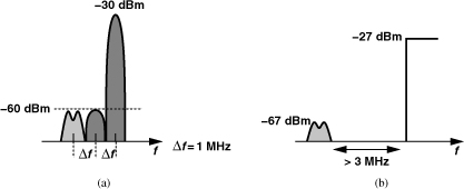
In Fig. 3.79(b), the desired signal is 3 dB above the sensitivity and a modulated blocker is applied in the third or higher adjacent channel with a power of −27 dBm. Thus, the 1-dB compression point of the receiver must exceed this value.
A Bluetooth receiver must also withstand out-of-band sinusoidal blockers. As shown in Fig. 3.80, with the desired signal at −67 dBm, a tone level of −27 dBm or −10 dBm must be tolerated according to the tone frequency range. We observe that if the receiver achieves a P1dB of several dB above −27 dBm, then the filter following the antenna has a relaxed out-of-band attenuation requirement.
Figure 3.80 Bluetooth receiver out-of-band blocking test.
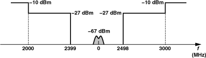
The intermodulation test in Bluetooth is depicted in Fig. 3.81. The desired signal level is 6 dB higher than the reference sensitivity and the blockers are applied at −39 dBm with Δf = 3, 4, or 5 MHz. In Problem 3.6, we derive the required RX IP3 and note that it is quite relaxed.
Figure 3.81 Bluetooth receiver intermodulation test.

Bluetooth also stipulates a maximum usable input level of −20 dBm. That is, a desired channel at this level must be detected properly (with BER=10−3) by the receiver.
3.7.5 IEEE802.11a/b/g
The IEEE802.11a/b/g standard allows high-speed wireless connectivity, providing a maximum data rate of 54 Mb/s. The 11a and 11g versions are identical except for their frequency bands (5 GHz and 2.4 GHz, respectively). The 11b version also operates in the 2.4-GHz band but with different characteristics. The 11g and 11b standards are also known as “WiFi.” We begin our study with 11a/g.
The 11a/g standard specifies a channel spacing of 20 MHz with different modulation schemes for different data rates. Figure 3.82 shows the air interface and channelization of 11a. We note that higher data rates use denser modulation schemes, posing tougher demands on the TX and RX design. Also, as explained in Section 3.3.6, for rates higher than a few megabits per second, wireless systems employ OFDM so as to minimize the effect of delay spread. This standard incorporates a total of 52 subcarriers with a spacing of 0.3125 MHz (Fig. 3.83). The middle subchannel and the first and last five subchannels are unused. Moreover, four of the subcarriers are occupied by BPSK-modulated “pilots” to simplify the detection in the receiver in the presence of frequency offsets and phase noise. Each OFDM symbol is 4 μs long.
Figure 3.82 IEEE802.11a air interface.
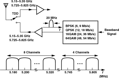
Figure 3.83 OFDM channelization in 11a.
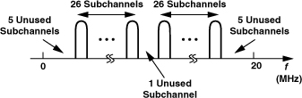
The TX must deliver a power of at least 40 mW (+16 dBm) while complying with the spectrum mask shown in Fig. 3.84. Here, each point represents the power measured in a 100-kHz bandwidth normalized to the overall output power. The sharp drop between 9 MHz and 11 MHz calls for pulse shaping in the TX baseband (Section 3.3.1). In fact, pulse shaping reduces the channel bandwidth to 16.6 MHz. The carrier frequency has a tolerance of ±20 ppm. Also, the carrier leakage must remain 15 dB below the overall output power.
Figure 3.84 IEEE802.11a transmission mask.
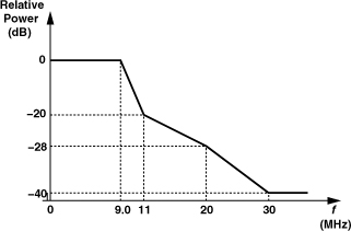
The receiver sensitivity in 11a/g is specified in conjunction with the data rate. Table 3.1 summarizes the sensitivities along with adjacent channel and alternate adjacent channel levels. The “packet error rate” must not exceed 10%, corresponding to a BER of less than 10−5.
Table 3.1 IEEE802.11a data rates, sensitivities, and adjacent channel levels.

The large difference between the sensitivities in Table 3.1 does make the receiver design difficult: the gain of the chain must reach about 82 dB in the low-rate case and be reduced to about 65 dB in the high-rate case.16
The adjacent channel tests shown in Table 3.1 are carried out with the desired channel at 3 dB above the reference sensitivity and another modulated signal in the adjacent or alternate channel.
An 11a/g receiver must operate properly with a maximum input level of −30 dBm. As explained for Bluetooth in Section 3.7.4, such a high input amplitude saturates the receiver chain, a very serious issue for the denser modulations used in 11a/g. Thus, the RX gain must be programmable from about 82 dB to around 30 dB.
The IEEE802.11b supports a maximum data rate of 11Mb/s with “complementary code keying” (CCK) modulation.17 But under high signal loss conditions, the data rate is scaled down to 5.5 Mb/s, 2 Mb/s, or 1 Mb/s. The last two rates employ QPSK and BPSK modulation, respectively. Each channel of 11b occupies 22 MHz in the 2.4-GHz ISM band. To offer greater flexibility, 11b specifies overlapping channel frequencies (Fig. 3.85). Of course, users operating in close proximity of one another avoid overlapping channels. The carrier frequency tolerance is ±25 ppm.
Figure 3.85 Overlapping channelization in 11a.
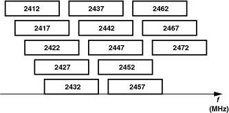
The 11b standard stipulates a TX output power of 100 mW (+20 dBm) with the spectrum mask shown in Fig. 3.86, where each point denotes the power measured in a 100-kHz bandwidth. The low emission in adjacent channels dictates the use of pulse shaping in the TX baseband. The standard also requires that the carrier leakage be 15 dB below the peak of the spectrum in Fig. 3.86.18
Figure 3.86 IEEE802.11b transmission mask.
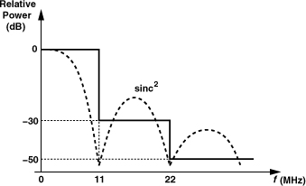
An 11b receiver must achieve a sensitivity of −76 dBm for a “frame error rate” of 8 × 10⁻² and operate with input levels as high as −10 dBm. The adjacent channel can be 35 dB above the desired signal, with the latter at −70 dBm.
3.8 Appendix I: Differential Phase Shift Keying
A difficulty in the detection of PSK signals is that the phase relates to the time origin and has no “absolute” meaning. For example, a 90° phase shift in a QPSK waveform converts the constellation to a similar one, but with all the symbols interpreted incorrectly. Thus, simple PSK waveforms cannot be detected noncoherently. However, if the information lies in the phase change from one bit (or symbol) to the next, then a time origin is not required and noncoherent detection is possible. This is accomplished through “differential” encoding and decoding of the baseband signal before modulation and after demodulation, respectively.
Let us consider binary differential PSK (DPSK). The rule for differential encoding is that if the present input bit is a ONE, then the output state of the encoder does not change, and vice versa. This requires an extra starting bit (of arbitrary value). The concept can be better understood by considering the implementation depicted in Fig. 3.87(a). An exclusive-NOR (XNOR) gate compares the present output bit, Dout(mTb), with the present input bit, Din(mTb), to determine the next output state:
![]()
implying that if Din(mTb) = 1, then Dout[(m + 1)Tb] = Dout(mTb), and if Din(mTb) = 0 then ![]() . The extra starting bit mentioned above corresponds to the state of the flipflop before the data sequence begins.
. The extra starting bit mentioned above corresponds to the state of the flipflop before the data sequence begins.
Figure 3.87 (a) Differential encoding, (b) differential decoding, (c) example of encoded and decoded sequence.
References
[1] L. W. Couch, Digital and Analog Communication Systems, Fourth Edition, New York: Macmillan Co., 1993.
[2] H. E. Rowe, Signals and Noise in Communication Systems, New Jersey: Van Nostrand Co., 1965.
[3] R. E. Ziemer and R. L. Peterson, Digital Communication and Spread Spectrum Systems, New York: Macmillan, 1985.
[4] P. A. Baker, “Phase-Modulated Data Sets for Serial Transmission at 2000 and 2400 Bits per Second,” Part I, AIEE Trans. Communication Electronics, pp. 166–171, July 1962.
[5] Y. Akaiwa and Y. Nagata, “Highly Efficient Digital Mobile Communication with a Linear Modulation Method,” IEEE J. of Selected Areas in Commnunications, vol. 5, pp. 890–895, June 1987.
[6] N. Dinur and D. Wulich, “Peak-to-average power ratio in high-order OFDM,” IEEE Tran. Comm., vol. 49, pp. 1063–1072, June 2001.
[7] T. S. Rappaport, Wireless Communications, Principles and Practice, New Jersey: Prentice Hall, 1996.
[8] D. P. Whipple, “North American Cellular CDMA,” Hewlett-Packard Journal, pp. 90–97, Dec. 1993.
[9] A. Salmasi and K. S. Gilhousen, “On the System Design Aspects of Code Division Multiple Access (CDMA) Applied to Digital Cellular and Personal Communications Networks,” Proc. IEEE Veh. Tech. Conf., pp. 57–62, May 1991.
[10] R. Kerr et al., “The CDMA Digitial Cellular System, An ASIC Overview,” Proceedings of IEEE CICC, pp. 10.1.1–10.1.7, May 1992.
[11] J. Hinderling et al., “CDMA Mobile Station Modem ASIC,” Proceedings of IEEE CICC, pp. 10.2.1–10.2.5, May 1992.
Problems
3.1. Due to imperfections, a 16QAM generator produces α1Ac cos(ωct+ Δθ)−α2Ac(1 + ![]() ) sin ωct, where α1 = ±1, ±2 and α2 = ±1, ±2.
) sin ωct, where α1 = ±1, ±2 and α2 = ±1, ±2.
(a) Construct the signal constellation for Δθ ≠ 0 but ![]() = 0.
= 0.
(b) Construct the signal constellation for Δθ = 0 but ![]() ≠ 0.
≠ 0.
3.2. Repeat Example 3.12 if the noise figure is less than 10 dB.
3.3. Repeat Example 3.12 for WCDMA.
3.4. Determine the maximum tolerable relative noise floor (in dBc/Hz) that an IMT-2000 TX can generate in the DCS1800 band.
3.5. Repeat Example 3.12 for the scenario shown in Fig. 3.73.
3.6. From Fig. 3.81, estimate the required IP3 of a Bluetooth receiver.
3.7. A “ternary” FSK signal can be defined as
![]()
where only one of the coefficients is equal to 1 at a time and the other two are equal to zero. Plot the constellation of this signal.
3.8. In order to detect (demodulate) an AM signal, we can multiply it by the LO waveform and apply the result to a low-pass filter. Beginning with Eq. (3.2), explain the operation of the detector.
3.9. Repeat the above problem for the BPSK signal expressed by Eq. (3.26).
3.10. The BPSK signal expressed by Eq. (3.26) is to be demodulated. As studied in the previous problem, we must multiply an cos ωct by an LO waveform. Now suppose the LO waveform generated in a receiver has a slight “frequency offset” with respect to the incoming carrier. That is, we in fact multiply an cos ωct by cos(ωc + Δω)t. Prove that the signal constellation rotates with time at a rate of Δω.