
Chapter 8
Libraries, Reusable Modules, and IP
Increasing electronic design density is a trend that has continued over the last 40 years. The consumer’s hunger for increasingly sophisticated gadgets, whether GPS, cellular telephones, games, home automation, networking, Internet commerce, audio/video entertainment, or computing, seems endless. We get more free time each year, and we are filling this time by playing with our electronic toys, all of which continue to get smaller, use less power, and grow more complicated. While the demand grows, the ability for industry to provide transistors and gates also seems endless. For the FPGA designer, this means designs will contain more gates.
Suppose an Engineer can design at a rate of 100 or so gates a day. Let’s call this about 10 lines of Verilog code (this includes the overhead of test and documentation). Soon, the average FPGA design will be 200,000 gates. This means, unless the design methodology changes, that a two-person team will take 1,000 days to complete a design, almost three years! Each year the design task gets more complex, but the schedule remains about the same. The company expects an average project to be complete in a year and a complex project to be complete in a year and a half. Clearly, something has to give. There are several options.
KEYS TO INCREASED PRODUCTIVITY
• The size of the design team must increase.
The most productive team is composed of one to three expert designers. If the company can afford to wait for the product, this will be the cheapest way to get it. However, most companies (in spite of what they say) are not interested in efficiency and productivity. Instead, they are interested in getting the product on the market as soon as possible. So, large teams are created upon the theory that if one woman can bear a child in nine months, then they’ll just have to get nine women to finish this job in one month.
The problem with large teams is that the complexity of the communication between team members increases exponentially as the number of team members increases linearly. If there are two team members, Jack and Jill, then Jack and Jill have to coordinate their work and there are two communication channels (Jack to Jill and Jill to Jack). If there are three team members, then Jack has to coordinate with Jill and Jerry, and Jill has to coordinate with Jack and Jerry, and so on, you get the idea. As confusing as this silly example is, real-life communication on a design team is worse.
It takes extraordinary effort to keep the team jelled and working in the same direction. Eventually, the design work of each team member must work with the design work of the other team members. This will not happen by accident. There will be more meetings (which reduces productivity), activity reports (which reduces productivity), more specifications to assure that design elements work together (which reduces productivity), and more chances of team conflict (which definitely reduces productivity).
Managing large teams is an art more than a science. Though the number of gates in a typical design is increasing exponentially, the ability for people to work together is not increasing much, if at all.
All is not lost; there is an alternative to creating large design teams.
• The individual designer must produce more code.
In the hardware design world, an electrical designer of the 40s designed with a handful of vacuum tubes. In the 50s, the tubes were replaced with transistors. In the 60s, the transistors were replaced with integrated circuits (100s of transistors). Today, ICs with millions of transistors are common. So, we hardware designers became comfortable with creating designs by mixing and matching circuit elements we didn’t design. There are two ways this can happen.
Each line of code can represent larger amounts of circuitry
As synthesis tools get smarter and FPGA designs get denser (so the number of gates required to implement a design becomes less important and we can afford to waste gates in order to produce a design more quickly), higher-level constructs become feasible. One day, we will implement a 1024-bit adder that runs at 100 MHz by writing a line of code like:
a = b + c;
Instead of handcrafting a look-ahead carry adder, the synthesis tool will infer an efficient adder based on your design constraints.
Designs will be reused
Modules will be included in your code from previous designs (the most common reuse method) or will be purchased or licensed from someone else. A lot of energy in our industry is focused on selling Intellectual Property (IP) designs to ASIC designers, and vendors would love to supply IP to the FPGA market, too. Frankly, the heavy-breathers in the ASIC and Design Automation areas think they will make large amounts of money selling designs to companies trying to reduce their product’s time-to-market.
If only there were a tried-and-true market model for using IP! Well, there is, and it’s related to the use of integrated circuits. This model has been used successfully for over 30 years, so it must work well. From a designer’s point of view, specifications, pricing, and delivery of various IP offerings are evaluated and the right product is selected for the design at hand. The financial model for the device manufacturer is interesting to consider. The device is designed at great expense and placed on the market. The up-front cost to produce this design (which can be millions of dollars) is paid back slowly over time as the devices are purchased by electronics manufacturers. This strategy can be quite profitable if the design becomes popular, but it takes deep pockets to play this game. Can IP vendors play this way?
The IP provider must provide complete data which characterizes performance including throughput, latency, signal I/O requirements, module size, and power consumption. This assures that the design is appropriate to the application and allows comparison to other products. The successful IP offering will be a stand-alone module that performs specific functions that designers are comfortable with, like FIFOs and other types of memory-based modules, microcontrollers, filters, compression/decompression functions, and communication ports (UARTs, Ethernet, USB, etc.). For even wilder speculation about the type of IP that might be feasible, see the Afterword: A Look into the Future, Millions and Millions and Millions of Gates.
Before we get too excited about off-the-shelf IP, lets take a look at the simplest method of increasing design productivity, the use of built-in library elements.
LIBRARY ELEMENTS
Each FPGA vendor supplies a set of primitive library elements. The Verilog design is mapped to the hardware using primitives similar to these. The primitives are implemented in an efficient manner by the underlying hardware. They get more capable every year as the FPGA vendor adds elements to, and increases the utility of, the libraries. The FPGA vendor has a vested interest in providing design aids and shortcuts that increase the efficiency and ease of use of their products.
The expert designer keeps in mind various levels of abstraction for a design, including the types of library elements that will be used to implement the design. The following is an example of what sort of elements we might see in a vendor’s primitive library:
There will be various flavors of these primitives. For example, the following versions of the AND gate might be available:
1. AND2 | 2-Input AND with Noninverted Inputs |
2. AND3 | 3-Input AND with Noninverted Inputs |
3. AND4 | 4-Input AND with Noninverted Inputs |
4. AND5 | 5-Input AND with Noninverted Inputs |
5. AND6 | 6-Input AND with Noninverted Inputs |
6. AND7 | 7-Input AND with Noninverted Inputs |
7. AND8 | 8-Input AND with Noninverted Inputs |
8. AND16 | 16-Input AND with Noninverted Inputs |
9. AND32 | 32-Input AND with Noninverted Inputs |
The Verilog compiler also uses a set of primitives. We see much similarity with the FPGA vendor primitive library.
1. FALSE
2. TRUE
3. INV
4. BUF
5. AND2
6. OR2
7. XOR2
8. NAND2
9. NOR2
10. MUX
11. DFFRS
12. DFFERS
13. LATRS
14. RSLAT
15. TRI
18. TRSTMEM
19. DON’T_CARE
The following device-specific library list is from Exemplar and is for the Xilinx 4000XL family. There is a similar library for generic primitives.
STRUCTURAL CODING STYLE
If you follow the digital design newsgroups (see the resources section), you will periodically see the schematic zealots presenting a case that efficient designs can generally be implemented only with schematics. This may be true, so, to the Verilog purist, it may make sense to do a schematic with text by wiring primitives together. Done properly, this will result in very compact and fast logic. However, it can get unwieldy very fast, so we’ll want to use this approach only where necessary.
One drawback of a schematic design can’t be argued: it’s not very portable. Using IP in a design requires some portability if the IP is to be offered for sale to the design world. IP and HDL need each other.
Listing 8-1 is an example of the structural use of a library primitive, Figure 8-1 shows the corresponding synthesized circuit, and Figure 8-2 shows the Xilinx structural resource assignment.
Listing 8-1 Verilog Structural Design with Library Primitive
// Structural Instantiation of Library Primitive.
module global_buffer (clock_out, data_out, chipsel, strobe,
data_in);
input chipsel, strobe, data_in;
output data_out;
reg data_out;
wire clock_in;
output clock_out;
assign clock_in = chipsel strobe;
BUFG buf1 ( .I(clock_in), .O(clock_out) );
endmodule
// Create black box for buffer.
module BUFG (I, O);
input I;
output O;
endmodule
Figure 8-1 BUFG Structural Resource Assignment
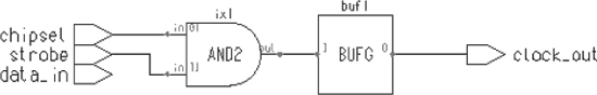
Figure 8-2 BUFG Structural Resource Assignment (information from Xilinx Floorplanning Tool)

Figure 8-2, a list of resources used in the global_buffer design, shows that BUF1 was implemented as a BUFGS (the only type of global buffer available in the Xilinx 4000XL family).
A SMALL DIVERSION TO COMPARE A SCHEMATIC TO A VERILOG DESIGN
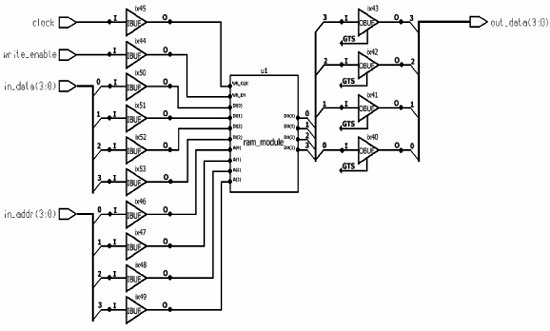
Figure 8-3 shows a schematic for a simple RAM implementation. It is interesting to compare this schematic with the Verilog structural version of this design as shown in Listing 8-2. More information on the LogiBLOX tool is presented in the next section.
Figure 8-3 Schematic Using Library Primitives

Listing 8-2 Verilog Structural Schematic Example
// Structural Schematic Design Example.
module schematic(out_data, in_data, in_addr, clock, write_enable);
input [3:0] in_data, in_addr;
input clock, write_enable;
output [3:0] out_data;
// Define the interface to the black box ram_module.
// This empty box will be filled with a predefined netlist
representing
// a RAM block created by the Xilinx LogiBLOX tool.
//----------------------------------------------------
// LogiBLOX SYNC_RAM Module Üram_moduleÜ
// Created by LogiBLOX version M1.5.19
// on Mon Dec 28 17:21:11 1998
// Attributes
// MODTYPE = SYNC_RAM
// BUS_WIDTH = 4
// DEPTH = 16
// STYLE = MAX_SPEED
// USE_RPM = FALSE
//----------------------------------------------------
ram_module u1 ( .A(in_addr), .DO(out_data), .DI(in_data),
.WR_EN(write_enable), .WR_CLK(clock) );
endmodule
module ram_module(A, DO, DI, WR_EN, WR_CLK);
input [3:0] A;
output [3:0] DO;
input [3:0] DI;
input WR_EN, WR_CLK;
endmodule
Figure 8-4 shows the LogiBLOX main menu.
Figure 8-4 Creating a RAM Module with LogiBLOX

Figure 8-5 shows the use of a LogiBLOX-generated module.
Figure 8-5 Structural Schematic using LogiBLOX RAM Module
Which is better, the HDL or the schematic? Which is faster to create, more portable, and easier to understand? Which is prettier? Which is more portable? Notice that the compiler inferred buffers as required to implement the design. These buffers must be instantiated by the designer in the schematic.
USING LOGIBLOX MODULE GENERATOR
How was the RAM module an example of increasing design speed? We didn’t invent a RAM module from scratch; we used a design tool to help create it. In this case, we used the Xilinx LogiBLOX tool to create it. Other modules can be created and parameterized, these include:
Accumulators
Adders/Subtractors
Clock Dividers
Comparators
Constants
Data Registers
Decoders
Inputs/Outputs
Memories
Multiplexers
Pads
Shift Registers
Simple Gates
Tristate Buffers
Employing these types of schematiclike elements in a structural design can allow the HDL designer to use hardware-specific hardware configurations options. For example, under the Tristate Buffer block definition, there are three options for pull-up resistor: none, pull-up, and double pull-up. Options like double pull-up are not directly supported by Verilog but may be required for some design implementations. The use of a structural design, where HDL is employed in a structural (schematic) fashion, or where Verilog modules are stitched together with schematics, may be required in some cases. Use whatever works!
So, one way to increase the number of gates we design in a day is to use a tool that automates the creation of certain types of modules.
Another Module Generator, the CORE Generator Tool
Xilinx (with the MEMEC company) provides a core generator with a wider variety of more complex modules compared to LogiBLOX. Examples of the functions include:
• FPGA Development Tools (DSP and FPGA development platforms for evaluation and benchmarking of DSP and FPGA designs).
• Processor peripherals including C2910A Bit Slice Processor core, DRAM controller, M8237 DMA Controller, M8254 Programmable Timer, M8255 Programmable Peripheral Interface, M8259 Programmable Interrupt Controller, XF8256 Multifunction Microprocessor Support Controller, and XF8279 Programmable Keyboard Display Interface.
• Processor products including IntellicoreTM Prototyping System, RISC CPU Core Demo, Scalable Development Platform, TX400 Series RISC CPU cores, and V8 uRISC Microprocessor.
• UARTS, including M16450, M16550A, and XF8250.
• Communication and Networking Cores, including ATM Cell Assembler, ATM Cell Delineation, ATM CRC10 Generator and Verifier, ATM CRC32 Generator and Verifier, ATM Utopia Slave (CC-141), Forward Error Correction Reed-Solomon Decoder/Encoder and Viterbi Decoder, Telecommunications HDLC Protocol Core, and Telecommunications MT1FT1 Framer.
• XF9128 Video Terminal Logic Controller.
• Standard Bus Interface Cores, including IEEE 1394 Firewire Link Layer Core, Firewire SuperLINK core evaluation board, 2 Wire Serial Interface, PCMCIA cores, USB cores.
• And others.
These cores are a mix of Xilinx-supplied modules (which are available for free) and third-party-supplied modules (which must be licensed). An example of the use of these cores is a design called sincos8 based on the 8X8 Sin/Cos LUT core model. The CORE Generator tool created a file called sincos8.vei, a Verilog interface file. This file defines the ports used by the core and provides an example of the module instantiation for use by the designer. The sincos8.vei file looks like Listing 8-3.
Listing 8-3 sincos8.vei File
module sincos8 (
ctrl,
theta,
c,
dout);
input ctrl;
input [7:0] theta;
input c;
output [7:0] dout;
endmodule
// The following is an example of an instantiation:
sincos8 YourInstanceName (
.ctrl(ctrl),
.theta(theta),
.c(c),
.dout(dout));
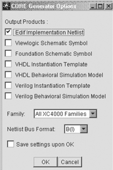
The CORE Generator file also created a Verilog simulation file called sincos8.v. This file is 5,287 lines of code. Assuming we could write 100 lines of debugged code a day, we could write this module in a couple of months. It took the CORE Generator about five seconds. Assuming the module meets the needs of the design, that’s not a bad leverage of productivity. If it doesn’t work, we don’t have any source code, so the core doesn’t help. The file we link into our design is the compiled EDIF netlist called sincos8.edf. Out of curiosity, let’s implement this design in a 4000XL device and see what it looks like. There are always some tricks to making the tools work; in this case, we need the bus delimiter to be parentheses B() (use B<> as delimiters for the XNF netlist format) in order for the Xilinx Design Manager to suck in the EDIF file properly. This is done by unchecking the Verilog Instantiation Template and Verilog Behavioral Simulation Model boxes (even though we want these files to be generated) in order to get the Netlist Bus Format we want as shown in Figure 8-6. In addition, in the Exemplar Leonardo EDIF output tab, we want to deselect the Allow Writing Busses checkbox, because Xilinx does not process EDIF busses properly.
Note that the Verilog compiler doesn’t “know” anything about the black box (which is inserted during the downstream mapping process, as illustrated in Figure 8-6). Any estimate by the synthesis tool regarding speed and design size will not include the black-box modules.
Figure 8-6 CORE Generator Options for Netlist Bus Format
Without really trying, this design runs at 61 MHz in the slowest 4005XL (-3) device. Listing 8-4 is a report on the resources used by this design.
Listing 8-4 sincos8 Design Example Resource Utilization
Loading device database for application par from file Ümap.ncdÜ.
sincos8_example is NCD, device xc4005xl, package pc84, speed -3
Loading device from file ‘4005xl.nph‘ in environment C:/Xilinx.
Device speed data version: x1_0.37 1.22 FINAL.
Device utilization summary:
Number of External IOBs 18 out of 61 29%
Flops: 0
Latches: 0
Number of CLBs: 25 out of 196 12%
Total Latches: 0 out of 392 0%
Total CLB Flops: 25 out of 392 6%
4 input LUTs: 43 out of 392 10%
3 input LUTs: 4 out of 196 2%
Number of TBUFs: 28 out of 448 6%
Another example is an eight-wide and 16-deep FIFO called fifo8x16. The Verilog simulation file is 293 lines of code. Listing 8-5 shows the interface file.
Listing 8-5 fifo8x16.vei File
module fifo8x16 (
d,
we,
re,
reset,
c,
full,
empty,
bufctr_ce,
bufctr_updn,
q);
input [7:0] d;
input we, re, reset, c;
output full;
output empty;
output bufctr_ce;
output bufctr_updn;
output [7:0] q;
endmodule
// The following is an example of an instantiation:
fifo8x16 YourInstanceName (
.d(d),
.we(we),
.re(re),
.reset(reset),
.c(c),
.full(full),
.empty(empty),
.bufctr_ce(bufctr_ce),
.bufctr_updn(bufctr_updn),
.q(q));
We can see that using a CORE generator is an effective way to create complex modules and increase design efficiency. This is a hit-or-miss process, because, if a module does not meet the needs of the design after trying all available compiler options, without source code there is no way to make modifications, so another approach will be required (like taking the time to design an optimized module from scratch).
DESIGN REUSE, REUSING YOUR OWN CODE
As you get some designs under your belt, you will find that you’ll reuse some of your design approaches and even certain modules. If you designed it, then you certainly understand its features and limitations and can make an almost instinctive judgment whether to reuse something or write it from scratch. What can you do to help make a design suitable for later use in other designs?
Designing Your Code for Reuse
• Document your work.
Use a header that describes the design from a toplevel. The header should describe input and output requirements and any tricks or quirks that are embedded in the design. Put in lots of comments, not just describing each line of code, but explaining the overall intent and strategy for problem solving.
• Use a version-control database product like SourceSafe or VCS.
Having a good database of old designs and following the discipline of using detailed comments for revisions can enhance the reusability of Verilog code. These products allow revisions to be “undone” and assure that a working version can be recovered. This feature alone can help you maintain your sanity when crunch time comes. These tools are even more critical when working with other designers.
• Partition logic into small modules.
Smaller modules, with dedicated specific functions, are more likely to be reusable than large, complex, and specialized modules.
• Use synchronous design techniques.
A synchronous design is more reliable and portable. For modules that must be asynchronous, put them in separate and well-documented modules; don’t mix them in with the synchronous areas of your code.
• Take a typing class.
You should either be infinitely patient or a good typist to create long and descriptive labels. If you’re a slow typist, you’ll never use easy-to-read and informative labels like video_output_enable_active_low. Your code will benefit from liberal use of real English. Try to use fewer acronyms and abbreviations.
• Don’t do odd things with the clock.
For example, try not to use gated clocks or both edges of a clock.
• Don’t use magic numbers.
Magic numbers are constants embedded in the code as so:
(test_pattern == 4’he; // Example of magic number (4’he).)
and they should generally be parameters so they can be changed at a top level or in an include file.
• Minimize Ports.
Module partitions should be selected to minimize interconnects between modules, particularly where clock domains are crossed. Like an orange, designs have natural boundaries for isolation and cohesion. Use these natural boundaries to partition the design. Split up complex modules into smaller and simpler parts.
• Don’t fix something unless it’s really broken.
If you see something in a working module that you don’t like, leave it alone. The possibility of inadvertently breaking something is so great that you must be absolutely sure there really is a problem before changing anything. Pretty code is not necessarily better code.
• Get some help with sticky problems.
If you have a problem and you’re not sure what to do, or you’re trying to select between competing options, talk to your peers about it. Get input from the newsgroups, Field Applications Engineers, or your neighbors—anywhere you can find it. Even if your cohorts have bad ideas, they may lead you to think about the problem in a different manner and may inspire a better approach. If you really can’t find help among your coworkers, then find a better bunch of people to work with.
• Archive Everything.
Keep scripts, make files, design notes, libraries, old versions, and all software used to compile and implement a design.
BUYING IP DESIGNS
What does an IP block look like? From a user’s perspective, the interface must be defined, including clock signals [polarity (uses of rising or falling edges or both), maximum and minimum frequencies, duty cycle, and loading], reset/preset signals (polarity, synchronous or asynchronous, required duration, and loading), and requirements for other ports.
The biggest issues with purchasing IP for an FPGA (I call this Revenue IP, some call it Silicon IP) are not technical but are related to negotiating a license. How much should the up-front payment be? How much for recurring payments (royalties)? What is the cost model for unexpected usage when product volumes are higher or lower than expected? How can usage be audited? How can the IP provider protect its investment and still provide enough data assure a successful implementation? These questions all must be addressed to make IP viable for a design.
Will Revenue IP (RIP) ever be a significant part of the FPGA designer’s life? As hardware designers, we are comfortable using hardware IP in the form of integrated circuits out of necessity. We are not ASIC designers, so we do not have to use expensive design tools and we don’t have direct access to the foundries. We could create a functionally equivalent design, but it would take more board space, take longer to design, and cost more to implement. Two of these three drawbacks are not present when our design ends up in an FPGA. We can argue with management that the last drawback, the time to do the design, will be balanced by the avoiding up-front costs or royalties. So, RIP is the right acronym for Revenue IP. We will use all the free (vendor-provided) and cheap (vendor-subsidized) IP we can get our hands on, but we will resist paying for other types of IP. Still, we need to take a look at the current IP strategies. For FPGAs, they come in two flavors: firm/hard and soft.
Hard or Firm IP
In the ASIC business, Hard IP is like a Standard Cell, a core that is predesigned and characterized for a specific foundry process. This option does not really exist for FPGAs; the closest we get is with Hard/Firm IP—prerouted and preplaced modules that can be linked with our other modules. Hard/Firm IP is most like using an integrated circuit in our design. It is a black box from a user’s point of view. The user can’t change it; it can only be plunked into a design and used as-is, with all other circuitry and routing forced around and through it. These modules are provided with a behavioral model that allows the design to be evaluated and tested. From a vendor’s point of view, this is the safest IP, as it is very difficult to reverse-engineer or to modify and present as a new design. From a user’s point of view, hard IP is not very friendly; it is a one-size-fits-all solution and allows no flexibility other than built-in configuration options. It’s not portable to new processes or technology without recompiling by the IP vendor.
Soft IP
From a user’s point of view, having source code that can be tweaked, hacked, and synthesized is much more desirable. But how then, can the IP vendor be assured of being paid? Get all the money up front? That’s not very likely. If a design ends up being 47% IP and 53% hacked by the user, what’s the right compensation? What keeps the designer from creating timing problems when the design (which can be very complex) is modified? Who is responsible in this situation?
To protect the IP vendor, Soft IP might be encrypted or obfuscated (comments removed, informative labels replaced with truncated and useless ones, and the code compressed to be unreadable) so that it can be synthesized and integrated into other parts of the design but not easily reverse-engineered.
SUMMING UP
The most common form of design reuse for FPGA designers will be reusing your own modules. We have covered some ways to design your code that will improve reusability. The next most common reuse method will be using modules designed by other engineers at your company; this avoids extra cost and legal issues. The most common tools for increasing productivity will be vendor-supplied libraries and core generation tools. Third-party IP will be a small part of the FPGA designer’s reuse strategy.