Chapter 4
More Digital Circuits: Counters, ROMs, and RAMs
This chapter presents an assortment of digital designs implemented with Verilog.
RIPPLE COUNTERS
The most common (generic) counter is a ripple counter, so described because the output ripples from stage to stage. If we create a Verilog counter like Listing 4-1, using the binary-counter option in Exemplar Logic LeonardoSpectrum’s Input File menu as shown in Figure 4-1, we’ll find the result is a synchronous binary counter.
Listing 4-1 Verilog Code for Simple Counter
module ripple1 (count_out, clk, reset);
input clk, reset;
output count_out;
reg [3:0] count_out;
always @ (posedge clk or posedge reset)
if (reset)
count_out <= 0;
else
count_out <= count_out + 1;
endmodule
Figure 4-1 Counter Style Selection
The problem with the ripple counter is that, because more than one output is changing at once, using combinational logic to decode output states results in glitchy signals. To avoid this problem, use counters like Gray Code, Johnson, or synchronous binary counters like Figure 4-1.
JOHNSON COUNTERS
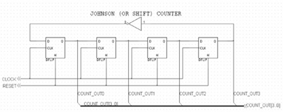
The Johnson counter is a type of shift counter. A shift counter uses little combinational logic to create the count logic and therefore can operate at high speed (the operating speed is limited only by how fast a flipflop can switch states and by the propagation delay of the simple count logic). The Johnson counter wraps an inverted version of the highest-order bit back to the lowest-order bit. Like the Gray Code counter, it has one output that changes at each clock. This results in a glitch-free output when decoded with combinational logic. Disadvantages include the requirement of more registers to store the count variable (around n/2 registers are required, where n is the max count value) and lack of error recovery. If a bad count pattern gets loaded, it will recirculate until the registers are reinitialized (if this ever happens!). The schematic for a Johnson counter is shown in Figure 4-2 with corresponding Verilog code in Listing 4-2 and count sequence in Listing 4-3.
Figure 4-2 Johnson Counter Schematic
Listing 4-2 Johnson Counter Verilog Code
module johnson1(clock, reset, count_out);
input clock, reset;
output count_out;
reg [3:0] count_out;
always @ (posedge clock or posedge reset)
if (reset)
count_out <= 0;
else begin
count_out[3:1] <= count_out[2:0];
count_out[0] <= ~count_out[3];
end
endmodule
Listing 4-3 Johnson Counter Output Sequence
0000
1000
1100
1110
1111
0111
0011
0001
0000
Repeat…
The alert designer notices that not all states are used in the count cycle. We have eight count states that are not used. Wasted counter states indicate that the design does not use registers efficiently, but this may not be important. However, if an illegal count occurs due to noise, there is no way to recover. Illegal states without recovery will make the careful designer nervous. Let’s add some logic, as shown in Listing 4-4, to detect and recover from those illegal states. This logic makes the counter a lot more complex, but it may be worthwhile to create a robust counter with glitchless output decoding.
Listing 4-4 Johnson Counter with Error Recovery
module johnson2(clock, reset, count_out);
input clock, reset;
output count_out;
reg [3:0] count_out;
always @ (posedge clock or posedge reset)
if (reset)
count_out <= 0;
// Add fault recovery.
else if (count_out == 4′h2) count_out <= 0;
else if (count_out == 4′h4) count_out <= 0;
else if (count_out == 4′h5) count_out <= 0;
else if (count_out == 4′h6) count_out <= 0;
else if (count_out == 4′h9) count_out <= 0;
else if (count_out == 4′ha) count_out <= 0;
else if (count_out == 4′hb) count_out <= 0;
else if (count_out == 4′hd) count_out <= 0;
else begin
count_out[3:1] <= count_out[2:0];
count_out[0] <= ~count_out[3];
end
endmodule
Another method of error recovery to consider is allowing an external device (like a microcontroller) to reinitialize the counter if an error occurs. Generally, software designers complain if the hardware staff creates logic that can’t be written to (or read from after a write occurs) by the software. Ability to read and write registers adds to the testability of the hardware, which is generally a good thing. This adds logic, which increases the design size and reduces the operating speed—bad things.
LINEAR FEEDBACK SHIFT REGISTERS
A type of counter that is quite interesting is a Linear Feedback Shift Register or LFSR counter. It is similar to the Johnson counter except that instead of an inverter from the last stage back to the first stage, a small number of taps are recycled. The counter next-state logic is very simple (a few XOR or XNOR gates). With maximal-length logic (taps selected to give the maximal count), a small number of registers can create counts of up to (2n)-1 (compared to a binary-counter count length of 2n). The one state that is missing from a maximal-length LSFR count sequence is the no-recovery state (all zeros for an XOR version or all ones for an XNOR version). An LFSR counter can operate at high speed compared to a binary counter because the feedback logic is very simple. For cases where the count value is arbitrary (the LFSR count sequence is pseudorandom) the LFSR counter can be a good solution.
How these can counters work can be illustrated by example. A maximal-length 4-bit LFSR counter can use the taps [3,0] (maximal length might be achieved with other taps, too). The taps are the register outputs that are fed back. Figure 4-3 has four flipflops and a single XNOR gate.
Figure 4-3 4-Bit LFSR Counter Schematic
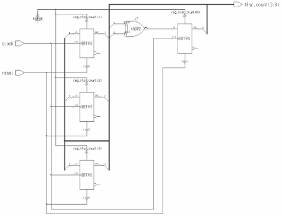
This version is sometimes called ‘many-to-one’; notice how taps are derived from many outputs, then XOR’d back to the input. There is also a variation called ‘one-to-many’ where all the feedback terms are combined before being fed back.
This counter of Listing 4-5 is an XNOR version. I generally use this version because the illegal state consists of all ones; I prefer to reset all registers on power-up (rather than preset some or all of the registers, which is necessary with the XOR version). Listing 4-6 presents a simple test fixture for testing the Verilog design of Listing 4-5.
Listing 4-5 Verilog Version of a 4-bit LFSR Counter
module lfsr4 (clock, reset, lfsr_count);
input clock, reset;
output lfsr_count;
reg [3:0] lfsr_count;
always @ (posedge clock or posedge reset)
if (reset)
lfsr_count <= 0;
else
begin
lfsr_count[3:1] <= lfsr_count[2:0];
lfsr_count[0] <= lfsr_count[3] ~^ lfsr_count[0];
end endmodule
Listing 4-6 Simple Test Fixture for 4-bit LFSR Counter
module lfsr4_tf(clock, reset, lfsr_count);
`timescale 1ns / 1ns
output clock, reset;
reg clock, reset;
input [3:0] lfsr_count;
parameter clk_period = 20;
lfsr4 u1 (clock, reset, lfsr_count);
always begin
#(clk_period / 2) clock = ~clock;
end
initial begin
clock = 0;
reset = 1; // Assert the system reset.
#75 reset = 0;
end
endmodule
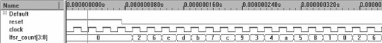
Figure 4-4 shows the count sequence for the 4-bit LFSR counter.
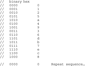
Figure 4-4 4-Bit LFSR Count Sequence
Looks like a big mess, doesn’t it? That’s part of the LFSR counter’s charm. Sequential values are loosely correlated, or pseudorandom. This can be useful for reducing clock harmonic noise. For example, in a binary counter, the lowest-order bit toggles on every clock; this results in noise that is highly correlated to the system clock and adds energy at subharmonics of the system clock. This harmonic energy is a large source of system noise. An LFSR counter generates more wideband noise with lower peak energy content, because the counter bits are changing in a more random manner.
Table 4-1 lists taps for maximal-length LFSR counters. Other tap selections are possible for some of the counter lengths.
Number of Bits | Length of Loop | Taps |
2 * | 3 | [1,0] |
3 * | 7 | [2,0] |
4 | 15 | [3,0] |
5 * | 31 | [4,1] |
6 | 63 | [5,0] |
7 * | 127 | [6,0] |
8 | 255 | |
9 | 511 | [8,3] |
10 | 1,023 | [9,2] |
11 | 2,047 | [10,1] |
12 | 4,095 | [11,5,3,0] |
13 * | 8,191 | [12,3,2,0] |
14 | 16,383 | [13,4,2,0] |
15 | 32,767 | [14,0] |
16 | 65,535 | [15,4,2,1] |
17 * | 131,071 | [16,2] |
18 | 262,143 | [17,6] |
Number of Bits | Length of Loop | Taps |
19 * | 524,287 | [18,4,1,0] |
20 | 1,048,575 | [19,2] |
21 | 2,097,151 | [20,1] |
22 | 4,194,303 | [21,0] |
23 | 8,388,607 | [22,4] |
24 | 16,777,215 | [23,3,2,0] |
25 | 33,554,431 | [24,2] |
26 | 67,108,863 | [25,5,1,0] |
27 | 134,217,727 | [26,4,1,0] |
28 | 268,435,455 | [27,2] |
29 | 536,870,911 | [28,1] |
30 | 1,073,741,823 | [29,5,3,0] |
31 * | 2,147,483,647 | [30,2] |
32 | 4,294,967,295 | [31,6,5,1] |
* indicates sequences whose length is a prime number
Sequences 2, 3, 5, 7, 13, 17, 19, 31 have lengths that are prime numbers.
This table is from Designus Maximus Unleashed by Clive Maxfield; it is copyrighted by Butterworth-Heinemann, 1998, and is used by permission.
Table 4-1 Maximal-Length LFSR Taps
From Table 4-1, you can see we can create a 31-bit counter with 31 registers and a single XOR gate. Imagine the ripple-carry logic required to create a 31-bit binary counter!
An example of the use of a LFSR counter is to create simple logic for a divide-by-N circuit. In this design, a terminal count is provided as an input to be compared to. Listing 4-7 illustrates an 8-bit divide-by-N counter, Listing 4-8 shows a test fixture, Listing 4-9 is the output list of the pseudorandom count sequence, and Figure 4-5 shows the waveforms at the count rollover.
Listing 4-7 Verilog Version of an 8-bit Divide-by-N LFSR Counter
// 8-bit Divide-by-N LSFR Counter.
module lfsr8 (clock, reset, lfsr_count, terminal_cnt, rollover);
input clock, reset;
input [7:0] terminal_cnt;
output lfsr_count;
reg [7:0] lfsr_count;
output rollover;
reg rollover;
always @ (posedge clock or posedge reset)
if (reset)
begin
lfsr_count <= 0;
rollover <= 0;
end
else
if (lfsr_count == terminal_cnt)// Test for terminal count.
begin
rollover <= 1;
lfsr_count <= 0;
end
else begin
rollover <= 0;
lfsr_count[7:1] <= lfsr_count[6:0];
lfsr_count[0] <= lfsr_count[7] ~^ (lfsr_count[3]
~^ (lfsr_count[2] ~^ lfsr_count[1]));
end
endmodule
Listing 4-8 Verilog Version of a 8-bit Divide-by-N LFSR Counter Test Fixture
// 8-bitit Divide-by-N LSFR Counter Test Fixture.
module lfsr8_tf(clock, reset, lfsr_count, terminal_cnt);
‘timescale 1ns / 1ns
output clock, reset;
reg clock, reset;
input [7:0] lfsr_count;
output [7:0] terminal_cnt;
reg terminal_cnt;
wire rollover;
parameter clk_period = 20;
lfsr8 u1 (clock, reset, lfsr_count, terminal_cnt, rollover);
always
begin
#(clk_period / 2) clock = ~clock;
end
initial
begin
clock = 0;
reset = 1; // Assert the system reset.
terminal_cnt = 8‘d66; // Test assignment.
#75 reset = 0;
end
endmodule
Listing 4-9 8-bit Divide-by-N LFSR Counter Count Sequence
lfsr_count = 00, rollover = 0 lfsr_count = 00, rollover = 0
lfsr_count = 00, rollover = 0 lfsr_count = 00, rollover = 0
lfsr_count = 01, rollover = 0 lfsr_count = 03, rollover = 0
lfsr_count = 06, rollover = 0 lfsr_count = 0d, rollover = 0
lfsr_count = 1b, rollover = 0 lfsr_count = 37, rollover = 0
lfsr_count = 6f, rollover = 0 lfsr_count = de, rollover = 0
lfsr_count = bd, rollover = 0 lfsr_count = 7a, rollover = 0
lfsr_count = f5, rollover = 0 lfsr_count = eb, rollover = 0
lfsr_count = d6, rollover = 0 lfsr_count = ac, rollover = 0
lfsr_count = 58, rollover = 0 lfsr_count = b0, rollover = 0
lfsr_count = 60, rollover = 0 lfsr_count = c1, rollover = 0
lfsr_count = 82, rollover = 0 lfsr_count = 05, rollover = 0
lfsr_count = 0a, rollover = 0 lfsr_count = 15, rollover = 0
lfsr_count = 2a, rollover = 0 lfsr_count = 55, rollover = 0
lfsr_count = aa, rollover = 0 lfsr_count = 54, rollover = 0
lfsr_count = a8, rollover = 0 lfsr_count = 51, rollover = 0
lfsr_count = a3, rollover = 0 lfsr_count = 47, rollover = 0
lfsr_count = 8f, rollover = 0 lfsr_count = 1f, rollover = 0
lfsr_count = 3e, rollover = 0 lfsr_count = 7c, rollover = 0
lfsr_count = f9, rollover = 0 lfsr_count = f3, rollover = 0
lfsr_count = e7, rollover = 0 lfsr_count = ce, rollover = 0
lfsr_count = 9d, rollover = 0 lfsr_count = 3a, rollover = 0
lfsr_count = 75, rollover = 0 lfsr_count = ea, rollover = 0
lfsr_count = d4, rollover = 0 lfsr_count = a9, rollover = 0
lfsr_count = 53, rollover = 0 lfsr_count = a6, rollover = 0
lfsr_count = 4c, rollover = 0 lfsr_count = 99, rollover = 0
lfsr_count = 33, rollover = 0 lfsr_count = 66, rollover = 0
lfsr_count = cd, rollover = 0 lfsr_count = 9a, rollover = 0
lfsr_count = 34, rollover = 0 lfsr_count = 68, rollover = 0
lfsr_count = d0, rollover = 0 lfsr_count = a0, rollover = 0
lfsr_count = 40, rollover = 0 lfsr_count = 81, rollover = 0
lfsr_count = 02, rollover = 0 lfsr_count = 04, rollover = 0
lfsr_count = 08, rollover = 0 lfsr_count = 10, rollover = 0
lfsr_count = 21, rollover = 0 lfsr_count = 43, rollover = 0
lfsr_count = 86, rollover = 0 lfsr_count = 0c, rollover = 0
lfsr_count = 19, rollover = 0 lfsr_count = 32, rollover = 0
lfsr_count = 64, rollover = 0 lfsr_count = c8, rollover = 0
lfsr_count = 91, rollover = 0 lfsr_count = 22, rollover = 0
lfsr_count = 44, rollover = 0 lfsr_count = 88, rollover = 0
lfsr_count = 11, rollover = 0 lfsr_count = 23, rollover = 0
lfsr_count = 46, rollover = 0 lfsr_count = 8d, rollover = 0
lfsr_count = 1a, rollover = 0 lfsr_count = 35, rollover = 0
lfsr_count = 6a, rollover = 0 lfsr_count = d5, rollover = 0
lfsr_count = ab, rollover = 0 lfsr_count = 56, rollover = 0
lfsr_count = ad, rollover = 0 lfsr_count = 5a, rollover = 0
lfsr_count = b5, rollover = 0 lfsr_count = 6b, rollover = 0
lfsr_count = d7, rollover = 0 lfsr_count = ae, rollover = 0
lfsr_count = 5d, rollover = 0 lfsr_count = bb, rollover = 0
lfsr_count = 76, rollover = 0 lfsr_count = ed, rollover = 0
lfsr_count = da, rollover = 0 lfsr_count = b4, rollover = 0
lfsr_count = 69, rollover = 0 lfsr_count = d2, rollover = 0
lfsr_count = a5, rollover = 0 lfsr_count = 4b, rollover = 0
lfsr_count = 97, rollover = 0 lfsr_count = 2e, rollover = 0
lfsr_count = 5c, rollover = 0 lfsr_count = b9, rollover = 0
lfsr_count = 73, rollover = 0 lfsr_count = e6, rollover = 0
lfsr_count = cc, rollover = 0 lfsr_count = 98, rollover = 0
lfsr_count = 31, rollover = 0 lfsr_count = 63, rollover = 0
lfsr_count = c6, rollover = 0 lfsr_count = 8c, rollover = 0
lfsr_count = 18, rollover = 0 lfsr_count = 30, rollover = 0
lfsr_count = 61, rollover = 0 lfsr_count = c3, rollover = 0
lfsr_count = 87, rollover = 0 lfsr_count = 0e, rollover = 0
lfsr_count = 1c, rollover = 0 lfsr_count = 39, rollover = 0
lfsr_count = 72, rollover = 0 lfsr_count = e4, rollover = 0
lfsr_count = c9, rollover = 0 lfsr_count = 93, rollover = 0
lfsr_count = 27, rollover = 0 lfsr_count = 4f, rollover = 0
lfsr_count = 9e, rollover = 0 lfsr_count = 3d, rollover = 0
lfsr_count = 7b, rollover = 0 lfsr_count = f7, rollover = 0
lfsr_count = ee, rollover = 0 lfsr_count = dd, rollover = 0
lfsr_count = ba, rollover = 0 lfsr_count = 74, rollover = 0
lfsr_count = e8, rollover = 0 lfsr_count = d1, rollover = 0
lfsr_count = a2, rollover = 0 lfsr_count = 45, rollover = 0
lfsr_count = 8a, rollover = 0 lfsr_count = 14, rollover = 0
lfsr_count = 28, rollover = 0 lfsr_count = 50, rollover = 0
lfsr_count = a1, rollover = 0 lfsr_count = 42, rollover = 0
lfsr_count = 00, rollover = 1 lfsr_count = 01, rollover = 0
Figure 4-5 8-Bit Divide-by-N LFSR Count Simulation at Rollover

The one-to-many variation as shown in Listing 4-10 splits the XOR (or XNORs) into 2-input gates and distributes them throughout the register array. Note: The same taps are used, simply in a different form. In words, the 4-bit counter taps [3,0] means: XOR (or XNOR) the output of register 0 and register 3 and connect that result to the input of register 1. The last register is wrapped back to register 0. This will still result in a maximal-length sequence, but the count sequence (and terminal count value for a given count) will be different. The schematic extracted from Listing 4-10 is shown in Figure 4-6. The output waveform is shown in Figure 4-7.
Figure 4-6 4-Bit LFSR One-to-Many Schematic

Listing 4-10 4-Bit LFSR One-to-Many Code
module lfsr4v2 (clock, reset, lfsr_count);
input clock, reset;
output lfsr_count;
reg [3:0] lfsr_count;
always @ (posedge clock or posedge reset)
if (reset)
lfsr_count <= 0;
else begin
lfsr_count[0] <= lfsr_count[3];
lfsr_count[1] <= lfsr_count[3] ~^ lfsr_count[0];
lfsr_count[3:2] <= lfsr_count[2:1];
end
endmodule
Figure 4-7 4-Bit LFSR One-to-Many Output Waveforms
For a more detailed explanation of LFSR counters, see Max Maxfield’s Designus Maximus Unleashed (details on this book can be found in the Bibliography).
CYCLIC REDUNDANCY CHECKSUMS
Logic similar to the LFSR is used to create Cyclic Redundancy Checksums, or CRCs. Checksums are used to test a data packet to try to determine if an error has occurred. An ordinary checksum simply adds up the data bytes or words and discards any carry beyond a predetermined resolution. For example, an 8-bit checksum would use modulo-256 addition and discard all carries that result in numbers greater than 255 (FF in hex).
Let’s assume a data packet consists of the following 8 bytes :
hex data
99
D0
01
09
83
AF
BE
We can use our hex calculator to find that the sum of these numbers is 40D(16). We discard all but the lower 8 bits and get a checksum of 0D. The receiving logic can do the same addition and see if the received data gives a checksum of 0D. This gives us some small confidence that the data was received correctly. What if we want more confidence? We could send a 16-bit checksum instead; this would give a 10-byte packet and a checksum of 40D. Now, for multiple errors, the chance of detecting an error is 1 in 65,536 instead of 1 in 256. If an error causes a number greater than expected in one byte and a later error causes a corresponding number the same amount less than expected, the checksum will match and we’ll think a bad packet is good. What if this is not good enough? A more random sequence of numbers would give us better error detection.
The idea behind a CRC is to do division instead of addition. The data packet is looked at as a huge binary number. We select a polynomial to divide this binary data with, and the remainder becomes our checksum. The sequence of remainders is more random than a sequence of sums. I’m going to skip a whole bunch of math and just tell you that logic to implement CRC division with a polynomial (where borrows are discarded) looks a lot like the logic which implements an LFSR. An input data packet is created with N bits of zeroes appended, where N is the length of the CRC, and is shifted out serially. While the data is transmitted, the CRC is calculated and then appended in place of the zeroes. This becomes the transmitted data packet.
At the receiver, the same CRC calculation is performed on the incoming data packet (including the CRC bits), and the remainder will be zero if no error is detected. Let’s illustrate this with a simple example. Xilinx uses a 16-bit CRC to validate the serial data used for FPGA configuration. The schematic for this logic is shown in Figure 4-8. Xilinx uses XOR logic, one-to-many configuration, and [15,14,1,0] feedback taps.
Figure 4-8 CRC-16 Schematic

Notice how similar this logic is to the LFSR with the addition of a data input as a modulation source. Listing 4-11 implements CRC-16 logic.
Listing 4-11 Verilog Version of CRC-16 Logic
module crc16 (clock, reset, serial_data_in, serial_data_out);
input clock, reset, serial_data_in;
output serial_data_out;
reg [15:0] crc_output;
assign serial_data_out = serial_data_in ^ crc_output[15];
always @ (posedge clock or posedge reset)
if (reset) crc_output <= 0;
else begin
crc_output[14:3] <= crc_output[13:2];
crc_output[1] <= crc_output[0];
crc_output[2] <= crc_output[1] ^ serial_data_out;
crc_output[15] <= crc_output[14] ^ serial_data_out;
crc_output[0] <= serial_data_out;
end
endmodule
ROM
ROM stands for Read-Only Memory. This memory is initialized when the FPGA is configured and cannot be changed after configuration (if it could be changed, then it would be RAM). As an example, we can implement the four-bit LFSR counter with a ROM if we want (we won’t want to if we have any sense, but we’ll do it anyway for the purpose of illustration); see Listing 4-12 and Figure 4-9.
Listing 4-12 ROM Version of LFSR Counter
2module lfsr_rom (binary_in, lfsr_out, clk, reset);
input [3:0] binary_in;
input clk, reset;
output [3:0] lfsr_out;
reg [3:0] lfsr_out;
always @ (posedge clk or posedge reset)
begin
if (reset)
lfsr_out <= 4′b0000;
else case (binary_in)
4′b0000: lfsr_out <= 4′b0000;
4′b0001: lfsr_out <= 4′b0001;
4′b0010: lfsr_out <= 4′b0010;
4′b0011: lfsr_out <= 4′b0101;
4′b0100: lfsr_out <= 4′b1010;
4′b0101: lfsr_out <= 4′b0100;
4′b0110: lfsr_out <= 4′b1001;
4′b0111: lfsr_out <= 4′b0011;
4′b1000: lfsr_out <= 4′b0110;
4′b1001: lfsr_out <= 4′b1101;
4′b1010: lfsr_out <= 4′b1011;
4′b1011: lfsr_out <= 4′b0111;
4′b1100: lfsr_out <= 4′b1110;
4′b1101: lfsr_out <= 4′b1100;
4′b1110: lfsr_out <= 4′b1000;
4′b1111: lfsr_out <= 4′b0000; // Unused combination.
//default:lfsr_out <= 4′b0; Not needed, all combinations covered.
endcase
end
endmodule
Figure 4-9 ROM Version of LFSR Counter Schematic

Because Xilinx implements combinations of four inputs very effectively, this function is efficient (not as efficient as the LFSR algorithm: the ROM version uses 2 CLBs, whereas our earlier design used 1 CLB). However, since the logic goes up by the square of the number of inputs, the ROM implemented in CLBs can get quite large. Another name for a ROM design like this is a Look-Up Table (LUT).
Many of the Xilinx CLBs have a RAM mode where a 16-by-1 memory element can be used in place of a CLB. This can be a very effective way to create RAM and ROM modules. We’ll explore the use of LogiBLOX and memory modules in Chapter 8. Something else to keep in mind is that many ASIC technologies do not have RAM capability. During ASIC conversion, ROM/RAM elements will be replaced with random logic, and this can result in a quite large ASIC design.
RAM
RAM stands for Random Access Memory, but that is not too helpful. A RAM is an array of memory (or storage) cells, addressable in groups N elements wide (data width, like x4, x8, x16, or x32) and M elements deep (number of N-width elements). We can synthesize a RAM out of CLBs, so let’s do a simple 16x1 block (a very tiny RAM block) and see how it looks. This design assumes that internal three-state drivers are available.
Note: One useful thing about the CLB RAM in an FPGA is the ability to initialize the RAM register cells on reset.
16x1 RAM block
There are 16 memory cells, so we need 2n = 16 addresses, or four address lines as shown in Listing 4-13.
Listing 4-13 Verilog 16x1 RAM Example Using Random Logic
module ram16x1(ram_data, ram_addr, ram_rwn, clock, reset);
inout ram_data;
input [3:0] ram_addr;
input ram_rwn, clock, reset; // Active low write.
reg [15:0] ram_data_reg;
wire ram_data_in;
assign ram_data = ram_rwn ? ram_data_reg[ram_addr] : 1′bz;
assign ram_data_in = ram_data;
always @ (posedge clock or posedge reset)
if (reset) ram_data_reg <= 0;
else case ({ram_addr, ram_rwn})
{4′h0, 1′b0} : ram_data_reg[0] <= ram_data_in;
{4′h1, 1′b0} : ram_data_reg[1] <= ram_data_in;
{4′h2, 1′b0} : ram_data_reg[2] <= ram_data_in;
{4′h3, 1′b0} : ram_data_reg[3] <= ram_data_in;
{4′h4, 1′b0} : ram_data_reg[4] <= ram_data_in;
{4′h5, 1′b0} : ram_data_reg[5] <= ram_data_in;
{4′h6, 1′b0} : ram_data_reg[6] <= ram_data_in;
{4′h7, 1′b0} : ram_data_reg[7] <= ram_data_in;
{4′h8, 1′b0} : ram_data_reg[8] <= ram_data_in;
{4′h9, 1′b0} : ram_data_reg[9] <= ram_data_in;
{4′ha, 1′b0} : ram_data_reg[10] <= ram_data_in;
{4′hb, 1′b0} : ram_data_reg[11] <= ram_data_in;
{4′hc, 1′b0} : ram_data_reg[12] <= ram_data_in;
{4′hd, 1′b0} : ram_data_reg[13] <= ram_data_in;
{4′he, 1′b0} : ram_data_reg[14] <= ram_data_in;
{4′hf, 1′b0} : ram_data_reg[15] <= ram_data_in;
default: ram_data_reg <= ram_data_reg;
endcase
endmodule
Figure 4-10 shows the schematic of the logic synthesized from Listing 4-13. Listing 4-14 summarizes the resources used by this design.
Listing 4-14 Design Summary for Verilog 16x1 RAM Example Using CLBs
Total accumulated area :
Number of BUFG : 1
Number of CLB Flip Flops : 16
Number of FG Function Generators : 29
Number of H Function Generators : 3
Number of IBUF : 7
Number of OBUFT : 1
Number of Packed CLBs : 15
Number of STARTUP : 1
***********************************************
Device Utilization for 4010xlPQ100
Resource Used Avail Utilization
-----------------------------------------------
IOs 8 77 10.39%
FG Function Generators 29 800 3.62%
H Function Generators 3 400 0.75%
CLB Flip Flops 16 800 2.00%
-----------------------------------------------
Clock Frequency Report
Clock : Frequency
clock : 41.1 MHz
Figure 4-10 Schematic for Verilog 16x1 RAM Example Using Random Logic

This illustrates how inefficient it is to implement RAM with FPGA CLBs. CLBs are designed to implement random logic functions. If we could replace this logic with a RAM cell, it would consume one CLB!
RAM elements are easy to create with Verilog. However, Verilog does not support two-dimensional arrays, so the RAM is modeled as a one-dimensional array of vectors.
Listing 4-15 is an example of a 256-by-8 synthesizable RAM module.
Listing 4-15 Verilog RAM Example
module ram_mod1(rwn, addr, data_port);
input rwn;
input [7:0] addr;
inout [7:0] data_port;
reg [7:0] ramdata [0:255];
assign data_port = (rwn) ? ramdata[addr] : 8′hz;
always @ (rwn or addr)
if (~rwn) ramdata[addr] = data_port;
endmodule
The RAM of Listing 4-15 will work, but unless the FPGA supports embedded RAM blocks, it will consume a huge amount of logic and be many times more expensive than any SRAM device you could buy. It might be all right for a tiny amount of RAM (on the order of 8 bytes), otherwise another solution must be found. Using flipflops to implement RAM is very inefficient.
Figure 4-11 Schematic for Verilog 256x8 RAM Example
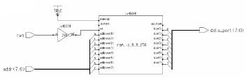
From Figure 4-11, you can see that Exemplar Logic LeonardoSpectrum correctly inferred a RAM from the Verilog code. In the Xilinx 4000XL family, embedded RAM is supported; see Figure 4-12. This schematic looks complicated, but compare it to Figure 4-13. The design in Figure 4-13 was compiled for an XC3000 device; this older device architecture does not have distributed CLB RAM. The schematic for the XC3000 implementation has 39 sheets!
Figure 4-12 256x8 RAM Implemented in the 4000XL Device Family, Sheet 1 of 1
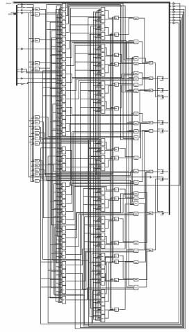
Figure 4-13 256x8 RAM Implemented in the XC3000 Device Family, Sheet 1 of 39

The designer often needs to implement RAM blocks to store an array of input or output data, configuration information, tables, or parameters. Many modern FPGA/CPLD architectures include RAM available as blocks (typical of Altera devices) or distributed across the device design so that a CLB can be configured as a LUT or as a RAM element (typical of Xilinx devices). You can see that using a single CLB as a 16-by-1 RAM cell is a good deal for the designer; it’s fast and doesn’t consume much of the FPGA resources.
What do you do if you need more than a trivial amount of RAM? There are two solutions. One is to pick an FPGA architecture that has enough built-in RAM to solve the problem (remember to leave yourself some wiggle room—if you need 1K of RAM, pick a device and architecture that has at least 2K available); the other is to put a real SRAM in the design. Though RAM blocks or distributed RAM cells are available in modern FPGAs, it is probably more expensive to use FPGA silicon for RAM than to use a real RAM IC. An additional consideration is the issue RAM raises during conversion to an ASIC.
Trade-offs Between Internal and External RAM
Internal RAM Features
• Speed. Not only are the RAM cells fast (in general), but we avoid the speed penalty of driving signals on and off the device.
• Timing. By staying on the chip, the clock/data relationship is known to the place-and-route tool. This eases our timing analysis. Internal FPGA signals are tweaked so the register hold time is zero. The external RAM may or may not have a zero hold time. Regardless, the delays associated with device I/O must be considered and will result in some sort of minimum hold time that must be accounted for in the design.
• Initialization. A nice feature of the FPGA RAM is the ability to initialize the RAM content on power-up. This initialization can be to write all zeros or to take RAM values from a file and store them in the RAM array. This can avoid requiring other means of initializing RAM (like having a microprocessor write to every location on power-up, for example).
Internal RAM Problems
• Cost. The silicon expended on internal RAM cells is probably more expensive than an external RAM device. The cost advantage is offset slightly by the cost associated with stuffing an extra device on the board and consuming extra FPGA pins.
Instantiating RAM
How do we instantiate RAM modules? Xilinx offers a tool called LogiBLOX for creating RAM modules, an example of a LogiBLOX module is shown in Listing 4-16. More detail on the procedure of creating a Xilinx LogiBLOX module is provided in Chapter 8.
Listing 4-16 Xilinx Synchronous Dualport RAM
module x_ram1 (clk, ram_data, ram_a_addr, ram_b_addr, ram_a_data,
ram_b_data, wr_strobe);
// Dualport RAM using Xilinx LogiBLOX.
input [15:0] ram_data;
input [4:1] ram_a_addr;
input [4:1] ram_b_addr;
input wr_strobe;
input clk;
output [15:0] ram_a_data;
output [15:0] ram_b_data;
//----------------------------------------------------
// LogiBLOX DP_RAM Module ![]()
![]() r16x16dp′′
r16x16dp′′
// Created by LogiBLOX version M1.3.7
// on Thu Feb 12 15:27:46 1998
// Attributes
// MODTYPE = DP_RAM
// BUS_WIDTH = 16
// DEPTH = 16
//----------------------------------------------------
r16x16dp ramblk1
(.A({ram_a_addr[4],ram_a_addr[3],ram_a_addr[2],ram_a_addr[1]}),
.SPO(ram_a_data),
.DI(ram_data),
.WR_EN(wr_strobe),
.WR_CLK(clk),
.DPO(ram_b_data),
.DPRA({ram_b_addr[4],ram_b_addr[3],ram_b_addr[2],ram_b_addr[1]}));
endmodule
The r16x16dp.vei module, shown in Listing 4-17, is simply a placeholder for the presynthesized netlist (r16x16dp.ngo) that will be inserted during the place-and-route process. It defines the module ports, but that is all. The interface part of this automatically generated file was cut and pasted into the module that instantiates the placeholder module. This .vei file must be included in Exemplar Logic LeonardoSpectrum’s input file list shown in Listing 4-16.
Listing 4-17 RAM Placeholder Module (r16x16dp.vei)
//----------------------------------------------------
// LogiBLOX DP_RAM Module “r16x16dp”
// Created by LogiBLOX version M1.5.19
// on Sun May 30 14:19:03 1999
// Attributes
// MODTYPE = DP_RAM
// BUS_WIDTH = 4
// DEPTH = 16
// STYLE = MAX_SPEED
// USE_RPM = FALSE
//----------------------------------------------------
module r16x16dp(A, SPO, DI, WR_EN, WR_CLK, DPO, DPRA);
input [3:0] A;
output [3:0] SPO;
input [3:0] DI;
input WR_EN;
input WR_CLK;
output [3:0] DPO;
input [3:0] DPRA;
endmodule
It’s easy to imagine using an external RAM in place of the LogiBLOX RAM; the difference is that module port pins must actually connect to device pins. An interesting expansion of the RAM interface occurs when multiple modules need RAM access. In this case an arbitration scheme can prioritize and negotiate access to the RAM. An example of external RAM interface with a simple arbiter (which allows multiple sources to access the RAM) is shown in Listing 4-18. There are probably better ways to implement this design, but this is a Real World example that was used in a commercial design.
Listing 4-18 RAM Access Interface and Arbitration Design
// arbit1.v © 1998 Advanced Technology Video, Inc.
// Reproduced with permission.
module arbit1 (clk, reset, chan0_ramaddr, chan0_dat_from_ram,
chan0_dat_to_ram, chan1_ramaddr, chan1_dat_from_ram,
chan1_dat_to_ram, address_preset, ram_rwn, ram_addr,
ram_data_pins, data_rd, data_wr, up_data_to_ram, up_data_from_ram,
sram_addr_strobe, rd_ack, wr_ack, ram_data_oe);
// System inputs.
input clk, reset; // System clock and reset.
// Control signals.
output [2:0] rd_ack; // Acknowledge: read complete.
reg [2:0] rd_ack;
output [2:0] wr_ack; // Acknowledge: write complete.
reg [2:0] wr_ack;
// RA M interface.
input [12:1] chan0_ramaddr;// Channel 0 RAM address pointer.
wire [12:1] chan0_ramaddr;
input [12:1] chan1_ramaddr;// Channel 1 RAM address pointer.
wire [12:1] chan1_ramaddr;
output [15:0] chan0_dat_from_ram;// Channel 0 RAM read data.
reg [15:0] chan0_dat_from_ram;
output [15:0] chan1_dat_from_ram;// Channel 0 RAM read data.
reg [15:0] chan1_dat_from_ram;
input [15:0] chan0_dat_to_ram; // Channel 0 RAM write data.
wire [15:0] chan0_dat_to_ram;
output [15:0] chan1_dat_to_ram; // Channel 1 RAM write data.
wire [15:0] chan1_dat_to_ram;
input [2:0] data_rd; // RAM read request.
wire [2:0] data_rd;
input [2:0] data_wr; // RAM write request.
wire [2:0] data_wr;
input sram_addr_strobe; // Preloads address counter.
input [15:0] up_data_to_ram; // Data written into RAM.
output [15:0] up_data_from_ram; // Data read from RAM.
reg [15:0] up_data_from_ram;
input [12:0] address_preset; // Microprocessor address
// counter preset input.
// RAM I/O ports.
output ram_rwn; // SRAM read/write, high = read.
output [12:0] ram_addr; // SRAM address pins.
reg [12:0] ram_addr;
inout [7:0] ram_data_pins;// RAM data to be written.
wire [7:0] ram_data_in;
reg [7:0] ram_data_out;
output ram_data_oe; // RAM output enable.
reg ram_data_oe;
// Local variables.
reg [3:0] ram_state;
reg ram_rdn;
reg [11:0] ram_addr_ctr;// Register: store auto-
// incremented addresses.
// Counts words.
parameter ram_state_idle = 0;
parameter ram_state1 = 1;
parameter ram_state2 = 2;
parameter ram_state3 = 3;
parameter ram_state4 = 4;
parameter ram_state5 = 5;
parameter ram_state6 = 6;
parameter ram_state7 = 7;
parameter ram_state8 = 8;
parameter ram_state9 = 9;
parameter ram_state10 = 10;
parameter ram_state11 = 11;
parameter ram_state12 = 12;
parameter ram_state13 = 13;
parameter ram_state14 = 14;
parameter ram_state15 = 15;
assign ram_rwn = ~ram_rdn; // Active high local signal.
// Control of SRAM data pins.
assign ram_data_pins = ram_data_oe ? ram_data_out : 8′bz;
assign ram_data_in = ram_data_pins;
always @ (posedge clk or posedge reset) begin
if (reset)
begin
ram_state <= ram_state_idle;
ram_rdn <= 0;
ram_addr <= 0;
ram_data_out <= 0;
rd_ack <= 0;
wr_ack <= 0;
ram_data_oe <= 0;
end else begin
case (ram_state)
ram_state_idle: begin
begin
ram_rdn <= 0;
ram_addr <= 0;
ram_data_out <= 0;
ram_data_oe <= 0;
end
if (data_rd[0]) begin
ram_rdn <= 0;
ram_addr <= {chan0_ramaddr, 1′b0};
ram_state <= ram_state1;
end
else if (data_rd[1]) begin
ram_rdn <= 0;
ram_addr <= {chan1_ramaddr, 1′b0};
ram_state <= ram_state3;
end
else if (data_wr[0]) begin
ram_rdn <= 1;
ram_addr <= {chan0_ramaddr, 1′b0};
ram_data_out <= chan0_dat_to_ram[7:0];
ram_data_oe <= 1;
ram_state <= ram_state5;
end
else if (data_wr[1]) begin
ram_rdn <= 1;
ram_addr <= {chan1_ramaddr, 1′b0};
ram_data_out <= chan1_dat_to_ram[7:0];
ram_data_oe <= 1;
ram_state <= ram_state8;
end
else if (data_rd[2])// Processor read request.
begin
ram_rdn <= 0;
ram_addr <= {ram_addr_ctr, 1′b0};
ram_state <= ram_state11;
end
else if (data_wr[2])// Processor write request.
begin
ram_rdn <= 1;
ram_addr <= {ram_addr_ctr, 1′b0};
ram_data_out <= up_data_from_ram[7:0];
ram_data_oe <= 1;
ram_state <= ram_state13;
end
else // Default.
ram_state <= ram_state_idle;
end
// Read channel 0.
ram_state1: begin
ram_rdn <= 0;
ram_addr <= {chan0_ramaddr, 1′b1};
chan0_dat_from_ram[7:0] <= ram_data_in;
rd_ack[0] <= 1; // Issue early.
ram_state <= ram_state2;
end
ram_state2: begin
ram_rdn <= 0;
ram_addr <= {chan0_ramaddr, 1′b1};
chan0_dat_from_ram[15:8] <= ram_data_in;
rd_ack[0] <= 1; // Hold ack until
// read is released.
if (data_rd[0])
ram_state <= ram_state2; // Hold until
// rd released.
else begin
rd_ack[0] <= 0; // Release ack.
ram_state <= ram_state_idle;
end
end
// Read channel 1.
ram_state3: begin
ram_rdn <= 0;
ram_addr <= {chan1_ramaddr, 1′b1};
chan1_dat_from_ram[7:0] <= ram_data_in;
rd_ack[1] <= 1; // Issue early.
ram_state <= ram_state4;
end
ram_state4: begin
ram_rdn <= 0;
ram_addr <= {chan1_ramaddr, 1′b1};
chan1_dat_from_ram[15:8] <= ram_data_in;
rd_ack[1] <= 1; // Hold ack until
// read is released.
if (data_rd[1]) // Hold until rd released.
ram_state <= ram_state4;
else begin
rd_ack[1] <= 0; // Release ack.
ram_state <= ram_state_idle;
end
end
// Write channel 0.
ram_state5: begin
ram_rdn <= 0;
ram_addr <= {chan0_ramaddr, 1′b0};
ram_data_out <= chan1_dat_to_ram[7:0];
ram_data_oe <= 1;
ram_state <= ram_state6;
end
ram_state6: begin
ram_rdn <= 1;
ram_addr <= {chan0_ramaddr, 1′b1};
ram_data_out <= chan1_dat_to_ram[15:8];
ram_data_oe <= 1;
wr_ack[0] <= 1; // Release early.
ram_state <= ram_state7;
end
ram_state7: begin
ram_rdn <= 0;
ram_addr <= {chan1_ramaddr, 1′b1};
ram_data_out <= chan1_dat_to_ram[15:8];
ram_data_oe <= 1;
wr_ack[0] <= 1; // Hold until write
// is released.
if (data_wr[0]) // Hold until wr released.
ram_state <= ram_state7;
else begin
wr_ack[0] <= 0; // Release ack.
ram_state <= ram_state_idle;
end
end
// Write channel 1.
ram_state8: begin
ram_rdn <= 0;
ram_addr <= {chan1_ramaddr, 1′b0};
ram_data_out <= chan1_dat_to_ram[7:0];
ram_data_oe <= 1;
ram_state <= ram_state9;
end
ram_state9: begin
ram_rdn <= 1;
ram_addr <= {chan1_ramaddr, 1′b1};
ram_data_out <= chan1_dat_to_ram[15:8];
ram_data_oe <= 1;
wr_ack[1] <= 1; // Release early.
ram_state <= ram_state10;
end
ram_state10: begin
ram_rdn <= 0;
ram_addr <= {chan1_ramaddr, 1′b1};
ram_data_out <= chan1_dat_to_ram[15:8];
ram_data_oe <= 1;
wr_ack[1] <= 1; // Hold ack until
// write is released.
if (data_wr[1]) // Hold until wr released.
ram_state <= ram_state10;
else begin
wr_ack[1] <= 0; // Release ack.
ram_state <= ram_state_idle;
end
end
// Microprocessor initiated read.
ram_state11: begin
ram_rdn <= 0;
ram_addr <= {ram_addr_ctr, 1′b1};
up_data_from_ram[7:0] <= ram_data_in;
ram_state <= ram_state12;
end
ram_state12: // Address counter incremented
begin // in this state.
ram_rdn <= 0;
ram_addr <= {ram_addr_ctr, 1′b1};
rd_ack[2] <= 1;
up_data_from_ram[15:8] <= ram_data_in;
ram_state <= ram_state_idle;
end
// Microprocessor initiated write.
ram_state13: begin
ram_rdn <= 0;
ram_addr <= {ram_addr_ctr, 1′b0};
ram_data_out <= up_data_to_ram[7:0];
ram_data_oe <= 1;
ram_state <= ram_state14;
end
ram_state14: begin
ram_rdn <= 1;
ram_addr <= {ram_addr_ctr, 1′b1};
ram_data_out <= up_data_to_ram[15:8];
ram_data_oe <= 1;
wr_ack[2] <= 1; // Release early.
ram_state <= ram_state15;
end
ram_state15: // Address counter incremented
begin // in this state.
ram_rdn <= 0;
ram_addr <= {ram_addr_ctr, 1′b1};
ram_data_out <= up_data_to_ram[15:8];
ram_data_oe <= 1;
wr_ack[2] <= 0;
ram_state <= ram_state_idle;
end
default: ram_state <= ram_state_idle;
endcase
end
end
// Increment address counter when microprocessor reads or writes.
always @ (posedge clk or posedge reset)
begin
if (reset) ram_addr_ctr <= 0;
else if (sram_addr_strobe)
ram_addr_ctr <= address_preset;
else if ((ram_state == ram_state12) |
(ram_state == ram_state15))
ram_addr_ctr <= ram_addr_ctr + 1;
end
endmodule
Modern synthesis tools can extract RAM from logic structures as long as we don’t bury them so deep that they are hard for the compiler to find. This means a random logic design is parsed and the compiler will try to extract modules that are more efficiently implemented as RAM blocks.
FIFO Notes
FIFOs (First-In First-Out memories) are used to change data rates between systems. Data is written at one rate and read out at a different (same or faster) rate. When you take your first look at a FIFO, it appears like a register file that expands and contracts like an accordion. However, it is really designed as a RAM block with an independent write address counter and an independent read address counter. For each FIFO write, the write counter (usually a Gray Code counter) gets incremented; for each FIFO read, the read counter gets incremented. The minimum set of flags includes an empty flag (set when the read and write pointers have caught up to each other and are equal) and a full flag (again set when the read and write flags are equal, but equal this time because the write address has wrapped around). The major goal of a FIFO system design is to prevent an overrun which results in data loss either due to new data not being written or old data being written over. The factors that influence overrun are the depth of the FIFO and the read and write frequencies.
One of the challenges of designing a FIFO is the flag design. The full flag, for example, is set in the write clock domain, but must be read and cleared in the read clock domain. This requires synchronization between the two domains, always a tricky task.
Like a RAM, a FIFO can be built out of registers. However, unless the FIFO is very small, you’re not going to want to build a FIFO out of registers (use RAM instead), because the design is inefficient.