
Chapter 2
Digital Design Strategies and Techniques
From a design entry point of view, the digital designer describes a design in as high a level of abstraction as possible. If it were possible to write one line of code that resulted in 25,000 gates of usable hardware (the day will come when a typical design is 2,500,000 gates), we’d agree that this is a very efficient way to do design work. We use sophisticated software tools to translate the abstract top-level design into a netlist that represents hardware and hardware interconnection.
The top-level design is processed in many steps before it is implemented in FPGA hardware. Each of these steps will be discussed in more detail later in this chapter.
DESIGN PROCESSING STEPS
• The design is parsed for syntax errors.
• The design is minimized and optimized for the target architecture.
• Recognized structure elements are replaced with library modules.
• Timing and resource requirements are estimated.
• The design is converted to a netlist.
• The design elements and modules are linked together and ‘black box’ modules are replaced with library or core module netlists.
• Floorplanning and routing attempts are made until the timing and resource constraints are met.
• Timing and resource reports are extracted from the design. A timing annotated netlist is created to support post-route simulation.
• The device configuration files are created.
ANALOG BUILDING BLOCKS FOR DIGITAL PRIMITIVES
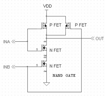
There will be many views of a design. The designer must be comfortable changing between different views of the same project as it evolves into a bitstream file formatted to configure an FPGA. It helps to keep in mind that all digital design elements are implemented with analog components. There is no magic device that acts like a NAND gate. We implement digital logic with analog devices like transistors, diodes, and resistors as shown in Figures 2-1, 2-2, and 2-3. Transistors can act as digital switches (on or off) or as analog transfer gates (pass mode). For the transistor impaired, N FETs are ON with a “one” on the gate, P FETs are ON with a “zero” on the gate.
Figure 2-1 Discrete Logic: Simplified Inverter

Figure 2-2 Discrete Logic: Simplified NAND Gate
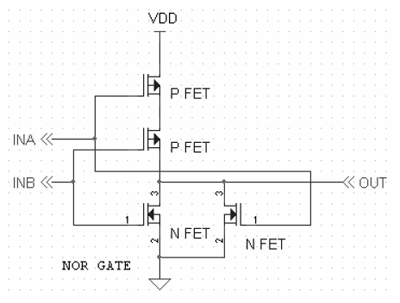
Figure 2-3 Discrete Logic: Simplified NOR Gate
USING A LUT TO IMPLEMENT LOGIC FUNCTIONS
Most FPGAs use a multiplexer (MUX) Look-Up Table (LUT) as a basic logic element. There are two reasons for doing this:
1. The LUT is versatile (any function of the inputs is possible)
2. The LUT is efficiently implemented in silicon.
The MUX control inputs are used as logic inputs, and the multiplex inputs are strapped to logic levels to implement the desired function. Figure 2-4 illustrates an inverter implemented using this method.
Figure 2-4 MUX Configured as an Inverter

A hidden advantage to using the MUX LUT as a logic element is provided by the capacitive loading and the “break-before-make” switching character of the MUX output. When the inputs change, the output is held and tends to change cleanly without glitching.
Synthesis Example
Changing back to the digital world, let’s refer to the Overheat Detector design of Chapter 1, reprinted here as Listing 2-1.
Listing 2-1 Overheat Detection Source Code
module overheat (clock, reset, overheat_in, pushbutton_in,
overheat_out);
input clock, reset, overheat_in, pushbutton_in;
output overheat_out;
reg overheat_out;
reg pushbutton_sync1, pushbutton_sync2;
reg overheat_in_sync1, overheat_in_sync2;
// Always synchronize inputs that are not phase related to
// the system clock.
// Use double-synchronizing flipflops for external signals
// to minimize metastability problems.
// Even better would be some type of filtering and latching
// for poorly behaving external signals that will bounce
// and have slow rise/fall times.
always @ (posedge clock or posedge reset)
begin
if (reset)
begin
pushbutton_sync1 <= 1′b0;
pushbutton_sync2 <= 1′b0;
overheat_in_sync1 <= 1′b0;
overheat_in_sync2 <= 1′b0;
end
else begin
pushbutton_sync1 <= pushbutton_in;
pushbutton_sync2 <= pushbutton_sync1;
overheat_in_sync1 <= overheat_in;
overheat_in_sync2 <= overheat_in_sync1;
end
end
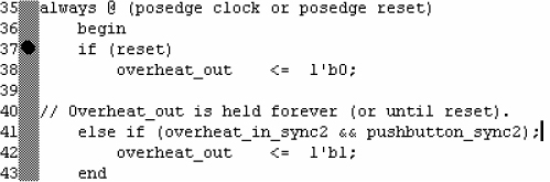
// Latch the overheat output signal when overheat is
// asserted and the user presses the pushbutton.
always @ (posedge clock or posedge reset)
begin
if (reset)
overheat_out <= 1′b0;
// Overheat_out is held forever (or until reset).
else if (overheat_in_sync2 && pushbutton_sync2)
overheat_out <= 1′b1;
end
endmodule
The synthesis tool converts our simple 40-line source code into an ugly EDIF netlist almost 300 lines long. This netlist holds all the design elements and information regarding the compiler version, target part, and all the design constraints the synthesizer knows about. This netlist is designed to be interpreted by other computer programs and doesn’t contribute much usable information to the designer, so we won’t look at an example.
A graphical version (a schematic) of the netlist as shown in Figure 2-5 is more useful to us in understanding what the synthesis tool created, particularly for the HDL impaired. Note the correct use of global resources for clock and reset. Because Verilog does not support direct assignment of hardware resources (the biggest problem for the Verilog FGPA designer), it is the designer’s job to assure that these inferences are made correctly.

Figure 2-5 Schematic Extracted from the EDIF Netlist
The synthesis tool has some understanding of the target architecture and can provide estimates of the design timing and resource requirement, see Listing 2-2. This estimate will not include black-box modules that are later imported by the FPGA place-and-route tool.
Listing 2-2 Synthesis Resource Estimate
*******************************************************
Cell: overheat View: INTERFACE Library: work
*******************************************************
Number of ports : 5
Number of nets : 13
Number of instances : 10
Number of references to this view : 0
Total accumulated area :
Number of BUFG : 1
Number of CLB Flip Flops : 2
Number of FG Function Generators : 1
Number of IBUF : 1
Number of IOB Input Flip Flops : 2
Number of IOB Output Flip Flops : 1
Number of Packed CLBs : 1
Number of STARTUP : 1
*******************************************************
Device Utilization for 4010xlPQ100
***********************************************
Resource Used Avail Utilization
-----------------------------------------------
IOs 5 77 6.49%
FG Function Generators 1 800 0.13%
H Function Generators 0 400 0.00%
CLB Flip Flops 2 800 0.25%
Clock Frequency Report
Clock : Frequency
------------------------------------
clock : 118.8 MHz
DISCUSSION OF DESIGN PROCESSING STEPS
Syntax Checking
The first step is to submit your code to a compiler, simulator, and/or Lint program that will identify syntax, typing, and other errors. Each program evaluates the code differently. If there is some confusion about what the syntax check says, it can be very helpful to try another interpreter. Listings 2-3 through 2-6 illustrate four ways that an error is reported for a simple problem inserted in the overheat.v code. A semicolon was appended on one of the if statements as so:
if (overheat_in_sync & pushbutton_sync);
Listing 2-3 Error Reporting by Exemplar LeonardoSpectrum Synthesis Tool
LeonardoSpectrum flagged “C:/Verilog/SourceCode/overheat.v”, line 37: Error, more than one sequential statement (if statement) in asynchronous process not supported.
Listing 2-4 Error Reporting by Model Technology ModelSim
ModelSim reported an error on the next line; at least in the right neighborhood of the error.
Listing 2-5 Error Reporting by Silos III
Reading “c:verilogverilogoverheat.v”
sim to 0
Highest level modules (that have been auto-instantiated):
(overheat overheat
c:verilogverilogoverheat.v (38) : error 3.229 : expecting
“end”, or statement, not integer constant
error 2.188 : errors are too severe to simulate
Listing 2-6 Error Reporting by Verilint
Processing source file c:verilogverilogoverheat.v
(E363) c:verilogverilogoverheat.v, line 37: Syntax error:
1 syntax error
End of interHDL inc. Verilint (R) Version 3.14, 1 errors, 0
warnings
The point of this exercise is to illustrate that different tools give different (and more or less useful) error messages, and it makes good sense to have several tools available for checking your code, particularly a Lint tool. Verilint (or a similar Verilog Lint tool) is useful because it’s fast, easy to use, and catches many different types of errors. This type of tool can save many hours of frustration. Regardless, this example illustrates how much trouble a single misplaced semicolon can cause.
Design Minimization and Optimization
The end result of all of our work is a configuration of hardware. This hardware can be an FPGA, a semicustom FPGA conversion, or some sort of ASIC (standard cell, gate array, full custom). If the result is an FPGA, the hardware will have an underlying structure that varies depending on the design approach taken by the FPGA vendor. The logic structure of a Xilinx 4K family is illustrated in Figure 2-6. We’ll take a closer look at this and other device architectures in Chapter 7.
The Xilinx 4K family Configurable Logic Block (CLB) is basically two 4-input LUTs feeding a pair of flipflops. The Verilog code we write gets mapped into this structure by the synthesis tool.

Figure 2-6 Typical Xilinx Configurable Logic Block Structure
The synthesizer translates the design to a form suitable for the target hardware by:
• Flattening the design into large Boolean equations with one equation for each module output, design section output, or register output. Redundant registers may be identified and optimized out. For example, the code fragment of Listing 2-7 might be flattened into the Boolean equation of Listing 2-8.
// Simple adder (no carry input).
module adder(clock, reset, a, b, c);
input clock, reset, a, b;
reg [1:0] c;
always @ (posedge clock or posedge reset)
begin if (reset)
c = 2’b0;
else
c = a + b; // Adder.
end
endmodule
To create the gate representation of this circuit, create a truth table (see Table 2-1) which defines all the input and output conditions.
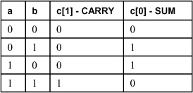
Table 2-1 Simple Adder Truth Table
By inspection, we see that the c[0] (SUM) output can be represented by an XOR gate and the c[1] output (CARRY) can be represented by an AND gate. A flattened version of the simple adder circuit is illustrated in Figure 2-7.
Listing 2-8 Simple Adder Boolean Equations
c[0] <= a ^ b;// ^ is the Verilog Boolean XOR operator.
c[1] <= a & b;// & is the Verilog Boolean AND operator.
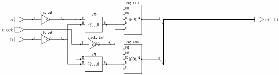
Figure 2-7 Flattened Schematic of Simple Adder Circuit
The logic mapped into the top F2_LUT to create c[0] (ix72) is (~I0 * I1) + (I0 * ~I1), equivalent to the XOR function. The logic mapped into the lower F2_LUT to create c[1] (ix71) is (I0 * I1).
• Minimizing the Boolean equations. This is done by recognizing and removing redundant logic terms (even if, for controlling fanout or providing hazard coverage, we want them to remain in the design).
The synthesizer can’t recognize redundant logic that crosses register boundaries (though it may recognize and delete redundant registers). If there is any chance for logic minimization, this must be part of the design input. The best opportunities for logic reduction are created and implemented by the designer.
• Recognized structure elements are replaced with selected modules. For example, the synthesizer might recognize a construct like a <= a – 1 as a down counter and replace the logic with a predefined circuit optimized for the target architecture for either area or speed.
• Timing and resource requirements are estimated. The compiler can only estimate the design timing and resource requirements. The manufacturer may have made changes to the timing parameters (the device manufacturer will always be ahead of other companies, who rely on the manufacturer for data). Another reason the timing estimate may not be accurate is that the library and black-box elements are not yet part of the design netlist. These elements are inserted when the design is linked and the final netlist is created and flattened.
• The design is converted to a netlist. There are various flavors of netlists, but the most common format at present is EDIF.
• The design elements and modules are linked together and ‘black-box’ modules are replaced with library module netlists. The netlist created by the compiler may be flattened (all the modules merged into one netlist) or the hierarchy may be maintained with the modules kept separate. With the hierarchy maintained, the design is easier for the designer to understand as it appears more like it was created.
• Floorplanning and routing attempts are made until the timing and resource constraints are met. Floorplanning assigns elements from the device logic to the designed circuitry. The place and route of the design is very much like the place and route of a printed circuit board. The efficiency of routing and the resulting speed of the routed design depend on the arrangement of the module elements, which affects the interconnect between modules. There are limited routing resources in an FPGA. When the routing gets dense (congested), long routing paths may be necessary to complete a signal path. This slows the design and causes routing problems for signals that must travel across or around the congested area. Some FPGA vendors advertise the capability of 100% routing of all logic, but others make densities of 65% (Altera) and 85% (Xilinx) more reasonable. Manual floorplanning can increase the usable logic density.
• Timing and resource reports are extracted from the design. A timing-annotated netlist may be created to support post-route simulation. A common format for a timing-annotated netlist is the SDF format as illustrated in Listing 2-9. SDF stands for Standard Delay Format. This file includes estimated gate delays based on the FPGA design rules.
Listing 2-9 Example of an SDF Netlist
(DELAYFILE
(SDFVERSION Ü2.0Ü)
(DESIGN ÜadderÜ)
(DATE Ü08/31/99 09:21:34Ü)
(VENDOR ÜExemplar Logic, Inc., AlamedaÜ)
(PROGRAM ÜLeonardoSpectrum Level 3Ü)
(VERSION Üv1999.1dÜ)
(DIVIDER /)
(VOLTAGE)
(PROCESS)
(TEMPERATURE)
(TIMESCALE 1 ns)
(CELL
(CELLTYPE ÜF2_LUTÜ)
(INSTANCE ix72)
(DELAY
(ABSOLUTE
(PORT I0 (::3.25) (::3.25))
(PORT I1 (::3.25) (::3.25)))))
(CELL
(CELLTYPE ÜF2_LUTÜ)
(INSTANCE ix71)
(DELAY
(ABSOLUTE
(PORT I0 (::3.25) (::3.25))
(PORT I1 (::3.25) (::3.25)))))
(CELL
(CELLTYPE ÜBUFGÜ)
(INSTANCE clock_ibuf)
(DELAY
(ABSOLUTE
(PORT I (::0.00) (::0.00)))))
(CELL
(CELLTYPE ÜOFDXÜ)
(INSTANCE reg_c_1)
(DELAY
(ABSOLUTE
(PORT C (::3.25) (::3.25))
(PORT D (::2.77) (::2.77)))))
(CELL
(CELLTYPE ÜOFDXÜ)
(INSTANCE reg_c_0)
(DELAY
(ABSOLUTE
(PORT C (::3.25) (::3.25))
(PORT D (::2.77) (::2.77)))))
(CELL
(CELLTYPE ÜIBUFÜ)
(INSTANCE reset_ibuf)
(DELAY
(ABSOLUTE
(PORT I (::2.77) (::2.77)))))
(CELL
(CELLTYPE ÜIBUFÜ)
(INSTANCE a_ibuf)
(DELAY
(ABSOLUTE
(PORT I (::2.77) (::2.77)))))
(CELL
(CELLTYPE ÜIBUFÜ)
(INSTANCE b_ibuf)
(DELAY
(ABSOLUTE
(PORT I (::2.77) (::2.77)))))
(CELL
(CELLTYPE ÜSTARTUPÜ)
(INSTANCE ix56)
(DELAY
(ABSOLUTE
(PORT GSR (::2.77) (::2.77)))))
)
• The device configuration files are created. The download file can be programmed into a serial EPROM, downloaded through a serial or parallel cable, or stored in memory and written to the device by a microprocessor, or by a stand-alone EPROM with address and data control generated by the FPGA itself. The device might be ISP (In-System Programmable) or a reprogrammable type (plugged into a programmer, programmed, then installed in the destination design).
Shifty Logic Circuits
Many people, when asked to draw a two-input NOR Gate, will draw a circuit that looks like Figure 2-8. In my experience this circuit seems shifty or flaky. This is not just a sign of mental illness. The output is very likely to be glitchy when the inputs change. We’re digital designers and we want the analog aspects of our design to be minimized.
Figure 2-8 Combinational Two-Input NOR Gate
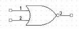
Figure 2-9 shows a typical circuit where the simple NOR gate might be used. The resistance and capacitance of Figure 2-9 do not have to be discrete devices on a circuit board, they could be parasitic values associated with signal routing and loading.
Figure 2-9 Simple Combinational Circuit
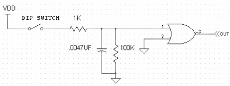
The oscilloscope trace shown in Figure 2-10 demonstrates one problem with the combinational circuit. One input is strapped low, so the output should just be the inverse of the other input, right? Where did those nasty glitches on the output come from? The input is a noisy signal that crosses the input threshold (where the input is between being recognized as one or zero by the gate input) very slowly. The RC network just exaggerates the problem and is exactly the kind of thing you see when some bonehead tries to filter out the switch contact bounce. The right way to filter switch bounce is to use feedback (hysteresis).
Figure 2-10 Combinational Two-Input NOR Gate Output Transients

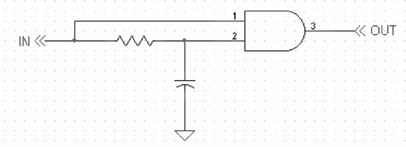
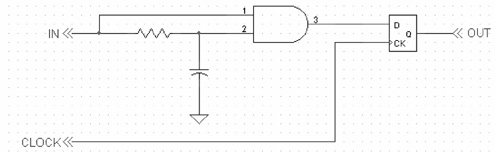
Fine, you say. You’ll make sure that the input always changes quickly to minimize glitches. So, you invent a circuit that switches infinitely fast (you can store this circuit on the same shelf as your perpetual motion machine). Anyway, that’s still not good enough, because there is another cause of glitches. When the inputs are changing at nearly the same time, again the output can be indeterminate. The circuit of Figure 2-11 demonstrates this problem. A resistor-capacitor (RC) network is added to delay the input signal. Again, the output has nasty transients. So, your design won’t use RC networks between inputs like this. Well, the RC time delay might be caused by mixed routing paths between inputs (signal skew) or by signal loading where each signal destination contributes a capacitive load. The R part of Figure 2-11 represents the sum of the source and routing impedance (proportional to route length) and the C part represents net loading (proportional to the number of loads on the net). The only control you have of this problem is making sure that signals have low fanout (a measure of the signal loading represented by destination logic elements where each gate load is counted as a fanout of 1). Most synthesis tools allow a fanout constraint to be defined to control loading (signals are split and driven by separate buffers).
Figure 2-11 Combinational Two-Input AND Gate with RC Network
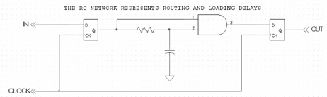
When I am asked to draw a two-input AND Gate, it looks like Figure 2-12. The difference is the addition of a synchronizing flipflop. The output of this circuit will not be glitchy if synchronous logic rules are followed and the setup/hold requirements for the flipflop are met (see the next section for a discussion of setup and hold times). This is particularly safe if the input signal is synchronous, too. If the signal at the D input of the flipflop is stable in time to meet the setup-time requirement and maintained beyond the hold-time requirement, then all is well.
Figure 2-12 Synchronous AND Gate
Synchronous Logic Rules
Metastability
Literally, metastability means beyond-settled? Something other than steady? If a signal is metastable, it is not stable, it is neither 1 nor 0, or it oscillates and will eventually resolve to a 1 or 0, but we don’t know which. As a digital designer, I hope this idea keeps you up late at night.
Metastability occurs when a clock edge is random with respect to a change of an asynchronous input signal. If the relation of the clock and signal is truly random, then it is inevitable that an input change will occur so close to a clock edge that the output is unpredictable. This problem manifests itself as a flipflop output that takes a long time to resolve, often much longer than the typical clock-to-Q output delay listed in the flipflop datasheet.
Figure 2-13 illustrates the metastability problem; if SIGNAL changes within the setup/hold window of the flipflop, the output is unknown for a period. How long is this period? It depends on the characteristics of the flipflop and its environment: how fast is the flipflop, how much gain does it have, and how much noise is present in the system. How big is this problem? It depends on how often the input changes and how wide the setup/hold window is compared to the clock period.
Figure 2-13 Metastable Output

We’ll never get to zero metastability, but hopefully the statistical probability of metastability will be microscopic. I don’t know about you, but if I can get the mean time between failures in my design to 100,000 years or so, that’s good enough.
The closest we will get to a solution to the metastability problem is to use synchronous design techniques. This means a synchronizing clock is used to qualify, gate, or trigger a circuit. The time between clock edges is used to allow signals to propagate and settle. It’s like a game; if you can get your signal to the next flipflop before the next clock setup time, then you win.
Setup and Hold Time
For the output of a flipflop to be predictable (not metastable), the inputs must meet the setup and hold time requirement of the flipflop.
• The setup time, often represented as Tsu, is the time period, BEFORE the edge of the synchronizing clock, when the input is required to be stable. If the setup time is violated, the output value is indeterminate.
• The hold time, often represented as Th, is the time period, AFTER the synchronizing clock edge, when the input is required to be stable. If the hold time is violated, again the output value is not guaranteed.
The setup and hold requirement comes from the analog nature of the flipflop design. The flipflop uses feedback implemented with cross-coupled gates to hold a state. It takes time for the gates to achieve their stable state. In a perfect world, an edge-triggered flipflop would change states exactly synchronous with the clock edge. The clock edge would be infinitely fast, and the flipflop would change states instantaneously. Real World clocks have rise/fall times, and flipflops require stable inputs during the setup/hold time to achieve a stable output state.
The flipflop metastability problem will never go away as long as a signal has a random phase relation to the flipflop clock. However, IC manufacturers have made great progress in closing the metastability window (this window is the setup plus hold time window). By increasing the speed of the flipflop, we make the metastability window narrower and less of a problem. The fact is, most problems that designers blame on metastability is related to asynchronous design technique. Each FPGA input should drive one and exactly one flipflop. The output of this single flipflop can be used to drive another flipflop for added security or can be used to drive the rest of your synchronous system. When an asynchronous input drives multiple flipflops, and the input changes near the clock edge, some flipflop outputs will change and some will not. This is not a metastability problem; this is an asynchronous input problem!
Figure 2-14 illustrates this. The RC delays represent signal delays due to routing and load inside the FPGA. We want all three flipflop outputs to be the same, but, depending on the phase of the input signal, sometimes the outputs will not be the same. If we synchronize the input with a single flipflop and do not violate its setup/hold time requirement, then all outputs are assured to be the same. That’s what we want!
Figure 2-14 Asynchronous Input Problem

How can we absolutely assure that the inputs are not going to change during the setup and hold period of the flipflop? The answer is an important part of the solution for the question: “How can I create a nearly trouble-free design?”
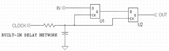
Figure 2-15 shows a synchronous AND gate with synchronous inputs.
Figure 2-15 Synchronous AND Gate with Synchronous Inputs
This goes a long way toward solving our problems, but the fussy among us might be asking why it works. It looks like the output of the synchronizing flipflops changes at a clock transition; isn’t that a problem for the output flipflop? Before we look at that, let’s consider a common circuit. If you were asked to design a divide-by-two circuit, you might draw something like Figure 2-16.
Figure 2-16 Divide-by-Two Circuit

This circuit could hardly be simpler; the inverting output is fed back to the D input, and the output changes state on every other clock edge. It is interesting to think about a situation where this circuit does not work. Let’s assume that the device technology has some easy numbers to work with, so all delays are 1 nsec.
Flipflop Specification:
Flipflop Minimum Input Setup Time: 1 nsec
Flipflop Minimum Input Hold Time: 1 nsec
Clock-to-Output Delay (Maximum): 1 nsec
Maximum Propagation Delay Time (Q output to D input) 1 nsec
For repeatable results, the D input must be stable 1 nsec before the clock edge and must remain stable after the clock edge for 1 nsec. The flipflop output is guaranteed to reach its final value less than 1 nsec after the clock edge. It takes less than 1 nsec for the signal to propagate from the Q output back to the D input. At what clock frequency does this circuit begin to fail?
Rising edges of the clock must not occur before setup time + output delay + routing delay, or 3 nsec. This means the input clock had better not have a frequency greater than 333.333 MHz. This is a high frequency, most likely achievable only with an ASIC using today’s technology. An FPGA will have longer (possibly much longer) delays and will have correspondingly lower maximum clock frequencies.
The delays for the device elements are provided by the device vendor. The number of delays can be mind-boggling. An FPGA has a complicated mix of delays; clock to Q, routing delays through switch elements, delays through signal multiplexers (look-up tables), and delays proportional to signal loading, among others. For example, for a 4000XL device, Xilinx specifies 41 timing parameters in 4 speed grades, for a total of 164 individual timing numbers. Memorize them; there will be a test later. Fortunately, the compiler knows these published delays and will calculate the totals for your circuit design. Let’s consider another simple circuit, two flipflops in series as shown in Figure 2-17.
Figure 2-17 Two Flipflops Connected in Series

Again, this is deceptively simple. How can this circuit work reliably? What if the minimum clock-to-output delay (a value that is rarely specified, but often estimated as 25% of typical) for U1 is less than the hold-time requirement for U2? So, you tear up your data book looking for the hold-time requirement, and with a sigh of relief (if you’re lucky) you see that it is specified as zero. The suspicious engineer will say, hold on a nanosecond, how can it be zero? All the logic circuitry we’ve ever looked at requires some hold time greater than zero. And that’s correct. It has to be so, but the designer of the FPGA logic cell has done some work for us and has put in delays to guarantee that the logic path (the logic in series with the D input) has a shorter delay than the clock path. Essentially, this is done by adding the hold time to the setup time, then delaying the clock enough to satisfy this extended setup time. With reference to the clock edge, the input signal takes longer to arrive at the D input, but it also stays around longer. Even if the input signal changes coincident with the clock edge, the clock delay inside the logic cell will make sure it stays valid long enough to satisfy the buried hold-time requirement of the flipflop. This simplifies the analysis of the FPGA design and assures that a circuit like Figure 2-18 will function.
Figure 2-18 Two Flipflops Connected in Series with Internal Delays
In summary, the FPGA chip designer has created a logic cell that assures the circuit of Figure 2-17 will work. ASIC designers don’t have this luxury and must account for delay and tolerance build-ups in their design. We do not have this luxury when dealing with signals from outside the FPGA. The signal characteristics of external signals must be examined and understood completely. If there is any sign of slow or glitchy signals, then we will implement circuits with hysteresis (like a Schmitt trigger) and will use a two-flipflop synchronizing circuit to minimize metastability.
Hysteresis is a circuit that adds positive feedback to the input. The idea is that when the output switches, it adds to the input to help prevent oscillation. The amount of feedback should be slightly greater than the noise on the input signal. Xilinx doesn’t widely advertise this information, but all their FPGA inputs have a few hundred millivolts of hysteresis; this makes their inputs friendly to noisy environments.
To complete our analysis, we must consider clock-skew. In a perfect world, all flipflops in our design will receive clock edges that are exactly synchronous. The first thing to understand is the clock-skew problem is not related to the operating frequency of your design! Even a slow design can have clock-skew problems.
Let’s expand the circuit of Figure 2-17 to show clock-skew, see Figure 2-19. Imagine that the flipflops are located far apart in the design and the second flipflop clock is delayed from the clock ‘seen’ by the first flipflop.
Figure 2-19 Two Flipflops Connected in Series with Clock Skew
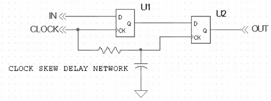
What is the problem? Let’s call t1 the clock-to-output delay period and t2 the propagation delay of the signal across the device to the D input of the second flipflop. We are hoping (and perhaps assuming) the value clocked into U2 is the old value of the Q output of U1. If the skew of the clock is too long, then we’ll get the new value at U1-Q—or worse, we’ll violate the setup or hold time requirement of U2 (depending on how much delay occurs) and get an unknown output from U2. We’re digital engineers; we don’t like unknowns. What is the solution? Fortunately, the FPGA designer provided low-skew clock networks carefully crafted to assure that the longest skew of the clock anywhere across the device is shorter than the shortest sum of clock-to-Q and signal routing propagation times. If you can use a global low-skew clock network, then there’s no problem. If you create an asynchronous design by using a routed clock (one that travels through random logic in the design), a gated clock, a MUX’d clock, or are designing an ASIC (where the clock networks are all custom designed), then you are responsible for assuring that this requirement is met.
Handling External Signals
We must also carefully analyze the situation where the FPGA designer has no control of one or more of the signals. Consider the case where an input source, represented by the flipflop U1 in Figure 2-17, is off-chip and is connected to a flipflop clocked by the FPGA clock. If U1 is a fast device, it is very possible that a race condition, which means signals arrive at synchronizing flipflops at different times, will occur. The race problem occurs when signals are changing at the input of a gate at the same time. This results in an unknown output. We’re digital designers; we like 1’s and 0’s. Unknown output states make us neurotic and twitchy.
This signal-race situation is much worse if there is no input-synchronizing flipflop in the input, because the race condition propagates across the design to all the circuits sensitive to the inputs. Very bad. At least, if there is an input-synchronizing flipflop, the only setup/hold time requirement is on that specific flipflop; once the timing is worked out for that device, the signal is well conditioned for operation inside the design. In a case like this, the easy solution is to make sure that the external device runs off the same clock as the logic synchronizing clock inside the design and is a slow device so the output can’t change fast enough to cause a race condition. Proving this can be a problem, because chip manufacturers almost never provide a minimum clock-to-Q output time. This is good for the manufacturers because it allows them to improve the IC process (make the device smaller, faster, and cheaper to build) without changing the data sheet. It’s bad for the designer using the parts who is diligently trying to do a worst-case timing analysis.
Using Alternate Clock Edges
A solution might be to clock external devices on the clock edge opposite to the one used inside the FPGA. Xilinx allows a flipflop to be clocked by either the rising or falling clock edge. Careful analysis must be done to assure that the timing works out. The clock-skew and setup time must be less than 1/2 a clock period compared to the full clock period allowed internal to the FPGA/ASIC design. A schematic of a circuit that uses the alternate clock edge is illustrated in Figures 2-20 with the resulting timing waveforms of Figure 2-21. Keep in mind that clocks never have perfectly equal high and low periods and these variations in duty cycle will subtract from the available flipflop setup time margin.
Figure 2-20 Two Flipflops Connected in Series Using Alternate Clock Edges

Figure 2-21 Two Flipflops Connected in Series Using Alternate Clock Edges, Timing Diagram

CLOCKING STRATEGIES
We’ve already decided that we want to create a synchronous design. This means there is at least one clock (preferably exactly one clock). Still, decisions remain about the clocking strategy used in the design. For the most trouble-free design, use one master clock. But what if the design has different clock domains it must interface with? What if using a single clock results in too much power consumption? There is no one answer to this problem; the answer depends on what you’re trying to accomplish. Here are some suggested clock strategies:
1. When designing an ASIC, if power consumption is NOT an issue, it’s best to use one master clock on all flipflops and replace lower-frequency clocks with clock enables to qualify logic wherever it makes sense to run at a lower frequency. Otherwise, just run at the master clock rate and be happy. This is the ideal situation. The design has one clock, which results in the simplest timing analysis. This design will be the easiest on which to use automated analysis and test tools. ATPG (Automatic Test Pattern Generation) works best on this type of design.
2. When designing an ASIC and power IS an issue (for battery operation or where the package power dissipation is a problem, for example), running flipflops with lower-frequency clocks in selected parts of the design is okay. The power consumed by a circuit is proportional to the clock frequency and the number of gates switching at the clock frequency. To reduce power consumption, make the design smaller and/or reduce the clock frequency. Minimize the amount of circuitry running at high speed. You are forced to deal with the problem of synchronizing signals crossing clock domains in exchange for reduced power consumption.
3. When designing an ASIC, but using FPGAs as prototypes, the desire would be to run with one master clock. This ties you to FPGAs that are fast and ASIC-like (Quicklogic, Actel, or some other antifuse One-Time Programmable type).
4. When designing an ASIC, and using FPGAs as prototypes, but using slow (that’s slow compared to ASIC processes) SRAM-based devices (like Xilinx or Altera) it would be desirable to run all flipflops off a single master clock, but you will probably be forced to run modules at the lowest possible speed to get the design to work. Drive flipflops with multiple clocks (divided or from external lower-frequency clocks), partition the design intelligently by creating the clocks in a central clock-generator module and minimizing the interconnect between clock domains, and make sure signals that cross clock domains are properly synchronized. Logic qualified with lower-frequency clocks used as clock enables will also work.
5. When doing a fast (by FPGA terms) FPGA design (which may become an FPGA-to-ASIC conversion), the best method is to use up the global clock resources, partition the design to minimize signals crossing clock domains, and synchronize signals properly. The FPGA-conversion folks routinely deal with multiple clocks. Some attention must be paid, but it’s a well-worn path.
6. When doing a slow FPGA design, thank your lucky stars and pick the method that works for you; either strategy is fine.
Clock Enable
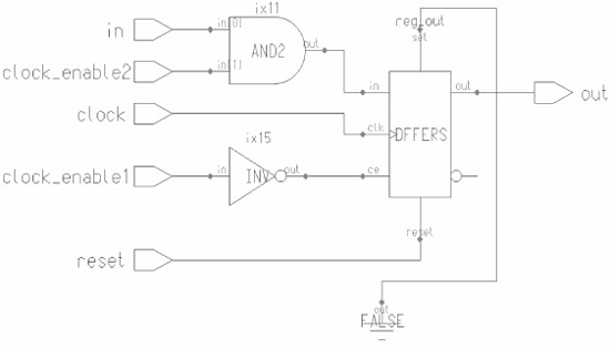
Verilog HDL does not support dedicated clock-enable signals. The hardware (FPGA or ASIC) may have dedicated clock-enable resources, but Verilog does not give direct control of this signal assignment. In the meantime, synthesis vendors will provide this support through compiler directives. This means that code like Listing 2-10, depending on whether the target hardware has dedicated clock-enable support, might synthesize in different ways. One way a design might be interpreted by the synthesizer is illustrated in Figure 2-22 where a clock-enable feature is available in the FPGA logic block design.
Listing 2-10 Clock-Enable Example
module clock_en(out,in,clock,clock_enable1,clock_enable2,reset);
output out;
input in, clock, clock_enable1, clock_enable2, reset;
reg out;
always @ (posedge clock or posedge reset)
begin if (reset)
Out <= 0;
else if (clock_enable1)
out <= out; // Hold output if not enabled.
elseout <= (in & clock_enable2);
end
endmodule
Figure 2-22 Synthesized Clock Enable
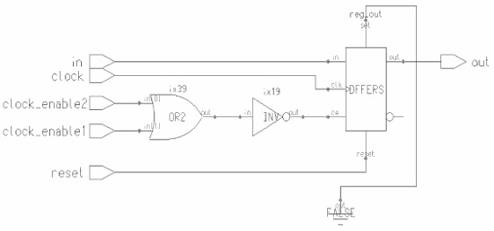
Some logic may get included in the logic that drives the clock enable, as shown in Figure 2-23. Note that the logic is not exactly the same; the point is that the synthesizer may insert added logic into the clock-enable path.
Figure 2-23 Synthesized Clock Enable (Mixed)
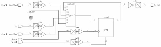
The next example, Figure 2-24, shows a clock-enable implemented in a technology that does not have a clock-enable feature in the logic block. The clock-enable is created with combinational feedback that holds the output when clock_enable is not asserted.
Figure 2-24 Synthesized Clock Enable (Routed)
LOGIC MINIMIZATION
A synthesizer can recognize and remove redundant logic. For example, the code fragments of Listings 2-11 and 2-12, are equivalent.
Listing 2-11 Redundant Logic Example 1 Code Fragment
input test1, test2, test3;
output sample;
sample = ((test1 & test2 & test3) | (test1 & !test2 & test3)
| (test1 & test2 & !test3));
Listing 2-12 Redundant Logic Example 2 Code Fragment
input test1, test2, test3;
output sample;
sample = (test1 & (test2 | test3));
The logic is minimized even if the designer intentionally put in the redundant logic to provide hazard coverage. Hazard coverage is the addition of redundant logic to cover up race conditions. This text will never suggest using hazard coverage; always use synchronous design techniques to avoid hazards.
The compiler can also recognize equivalent logic equations. An alternate form of an equation might use less area or fewer levels of logic when implemented in an FPGA. The compiler will try alternate equation forms and use the equation that best meets the design requirements.
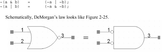
DeMorgan’s Theorems
~(a & b) = (~a | ~b);
~(a | b) = (~a & ~b);
Schematically, DeMorgan’s law looks like Figure 2-25.
Figure 2-25 Schematic Form of DeMorgan’s Law
There is a corollary to the AND/OR form that can be applied to the exclusive-OR form:
a ^ b = ~a ^ ~b;
~(a ^ b) = ~a ^ b = a ^ ~b;
AND/OR functions are duals of each other (like division is the dual of multiplication). DeMorgan’s law defines the conversion between the AND/OR equation forms.
The compiler can also manipulate equations using the laws of Boolean algebra. These laws are:
Commutative Law
a | b = b | a;
Associative Law
a | (b | c) = (a | b) | c;
Distributive Law
a & (b | c) = (a & b) | (a & c);
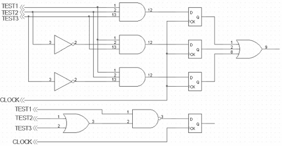
Because the designer uses synchronous techniques and doesn’t clog up the design with complicated structures between registers, the ability of the synthesis tool to extract redundant logic is limited. There may be simpler logic, but the synthesizer will not be able to extract it if the logic is spread across register boundaries. Examine Figure 2-26, which implements the logic of Listing 2-11 with synchronous techniques. The synthesizer will not find the redundancy! Except for some propagation delays, the two circuits shown in Figure 2-26 are equivalent.
Figure 2-26 Redundant Logic Terms Spread across Register Boundaries
The best logic synthesizer is the one between your ears. A poorly planned design will always be poor regardless of how great the compilers become. When doing a design, a good designer keeps a model of the synthesized logic in her head and doesn’t allow the logic to grow so complex that it becomes a problem for the synthesis tool. One way of taking advantage of the synthesis tool’s capability to minimize and pack logic effectively is to never create purely combinational modules. None of the popular FPGA architectures have purely combinational logic elements. There is generally a register that goes wasted if a CLB is used only for combinational logic. Mix the combinational logic with the synchronous logic to allow the synthesis tool to merge the logic into the resources available in the device. The logic block architecture uses combinational logic or LUTs (Look-Up Tables) that feed into registers. Write your logic that way!
Figure 2-27 Combinational Logic Clouds Feeding Flipflops

Notice how the logic of Figure 2-27 is partitioned into modules.
WHAT DOES THE SYNTHESIZER DO?
It’s helpful to think about what the synthesizer is doing. The synthesis tool takes Verilog HDL and maps it into hardware. First, the synthesizer will minimize logic equations by removing redundant logic terms. Then the design will be a huge set of Boolean equations. The remaining problem can be thought of as a simple division:
A/B
where A is the full design and B represents the hardware elements available in the target CPLD, FPGA, or ASIC. In general, for a CPLD the hardware structure will be multi-input Logic Elements (LE), for an FPGA the hardware structure will be a 3- or 4-input look-up tables (LUT), and for an ASIC the hardware structure will be a more freeform collection of library elements. Assuming the basic logic element is a 4-input LUT, the synthesis tool will partition our complicated denominator into many equations, each a function of 4 inputs. There will be many sets of equations that will implement our design, and the synthesis tool will attempt to find ones that meet the design goals of size and speed.
A truth table lists all input combinations and defines an output condition for each. A truth table is a tabular equation form and works well for software manipulation of equations. The compiler will extract a sum-of-products (SOP) equation from your HDL code. The SOP is developed by collecting terms that give a 1 result and ORing them together.
Let’s do a SOP representation of a 7-segment decoder. This decoder, similar to a CMOS 4513, will convert 4-bit binary-coded decimal (BCD) number to device pins that drive a 7-segment display.
Here is the truth table:
Input Segment
BCD a b c d e f g
b3 b2 b1 b0
0 0 0 0 1 1 1 1 1 1 0
0 0 0 1 0 1 1 0 0 0 0
0 0 1 0 1 1 0 1 1 0 1
0 0 1 1 1 1 1 1 0 0 1
0 1 0 0 0 1 1 0 0 1 1
0 1 0 1 1 0 1 1 0 1 1
0 1 1 0 1 0 1 1 1 1 1
0 1 1 1 1 1 1 0 0 0 0
1 0 0 0 1 1 1 1 1 1 1
1 0 0 1 1 1 1 1 0 1 1
Let’s collect the input terms that cause the ‘a’ segment to be asserted.
a = ((!b3 & !b2 & !b1 & !b0) | (!b3 & !b2 & b1 & !b0)
| (!b3 & !b2 & b1 & b0) | (!b3 & b2 & !b1 & b0)
| (!b3 & b2 & b1 & !b0) | (!b3 & b2 & b1 & b0)
| ( b3 & !b2 & !b1 & !b0) |( b3 & !b2 & !b1 & b0));
We can get a hint about how the reduction algorithm works by extracting and examining two terms of the equation:
(!b3 & !b2 & !b1 & !b0)|(b3 & !b2 & !b1 & !b0)=(!b2 & !b1 & !b0);
The equation terms differ only in the b3 term, which is asserted low in the first term and asserted high in the second. Clearly the b3 term doesn’t matter, is redundant, and can be removed without affecting the logic.
Next we’ll convert the ‘a’ segment equations to standard decimal-sum form by replacing all negated terms with 0 and all true terms with 1. A term like (!b3 & !b2 & !b1 & !b0), which has all terms negated, becomes (0,0,0,0), and the whole term can be represented by a decimal 0. The next term, (!b3 & !b2 & b1 & !b0), (0,0,1,0) becomes 2, and so on, until we collect all the terms that lead to the ‘a’ segment being asserted:
a = (0,2,3,5,6,7,8,9)
This form of the Boolean equation is used in the Quine-McCluskey method of reducing logic equations.
The Quine-McCluskey algorithm arranges terms in order of the number of the (0) terms. Only terms whose total numbers of negated terms differ by 1 can possibly be combined. For example, when we combined (0,0,0,0) with (1,0,0,0), this combination was possible because the first term has 4 zeros and the second term has 3 zeros. The Quine-McCluskey algorithm exhaustively tests terms and combined terms against each other to determine the minimum logic expression.
Running QM with the logic terms for segment ‘a’ gives the reduced equation:
a =((!b3 & !b2 & !b0)|(b3 & ! b2 & !b1)|(!b3 & b2 & b0)|(!b3 & b1));
Let’s see if we can follow what the synthesizer does with this logic defined as a Verilog design in Listing 2-13.
Listing 2-13 Verilog Design for 7-Segment Display Decoder ‘a’ Term
module seven_seg (clk, reset, bcd_input, a_segment);
input clk, reset;
input [3:0] bcd_input;
output a_segment;
reg a_segment;
always @ ( posedge clk or posedge reset)
if (reset)
a_segment <= 0;
else
begin case (bcd_input)
{1’b0, 1’b0, 1’b0, 1’b0}: a_segment <= 1’b1;
{1’b0, 1’b0, 1’b0, 1’b1}: a_segment <= 1’b0;
{1’b0, 1’b0, 1’b1, 1’b0}: a_segment <= 1’b1;
{1’b0, 1’b0, 1’b1, 1’b1}: a_segment <= 1’b1;
{1’b0, 1’b1, 1’b0, 1’b0}: a_segment <= 1’b0;
{1’b0, 1’b1, 1’b0, 1’b1}: a_segment <= 1’b1;
{1’b0, 1’b1, 1’b1, 1’b0}: a_segment <= 1’b1;
{1’b0, 1’b1, 1’b1, 1’b1}: a_segment <= 1’b1;
{1’b1, 1’b0, 1’b0, 1’b0}: a_segment <= 1’b1;
{1’b1, 1’b0, 1’b0, 1’b1}: a_segment <= 1’b1;
default: a_segment <= 0;
endcase
end
endmodule
For Xilinx 4xxx logic, which uses a 4-input LUT feeding a flipflop as a primitive, the synthesizer arranges the logic to efficiently use the CLB resources and gives the circuit of Figure 2-28 for the ‘a’ logic.
Figure 2-28 Synthesized Logic for 7-Segment Display Decoder ‘a’ Term Logic

AREA/DELAY OPTIMIZATION
When implementing a design, there are two fundamental properties: how big is it and how fast will it operate? Synthesizing a logic design is much like autorouting a circuit board. When routing a circuit-board trace, there are many options. Which path should the signal take? What is the signal priority compared to other signals? There is no one answer. The circuit-board trace can take a nearly unlimited set of paths to its destination. The right answer occurs when the routing has met the requirements of the design, even if it’s possible to get better area/delay performance. This bears special emphasis. The designer’s work will not be judged by how perfect it is! The designer’s work will be judged by how well it meets the system requirements for product cost, development cost, performance, reliability, maintainability, and time to market. The quest for perfection will not be rewarded. The goal of our quest is to achieve ‘good enough.’ This does not mean we’re going to deliver a bad design. Our design still must meet timing requirements and use good design practices.
The concept of design cost weighs area and speed (delay) against each other. In many cases, the fastest design is not the smallest. In many cases, the smallest design is not the fastest. The designer has successfully accomplished the design if it fits into the technology selected and runs fast enough to meet the needs of the system. How easy or difficult this problem is depends on many factors: the size of the selected device, the architecture of the device technology, the system speed requirement, and the skill and design approach of the designer.
The experienced designer always leaves a way out of a problem by insuring that a faster or denser device, if at all possible, is available in the same device footprint.
This way, instead of redesigning a circuit board to accommodate a new device at great expense and loss of time, a faster and/or denser device can be easily substituted.