
Chapter 9
Designing for ASIC Conversion
There are some advantages to converting an FPGA design to an ASIC, including merging multiple FPGAs into one ASIC and creating a device that consumes less power and operates at higher speeds. However, the main advantage is reducing cost. The cost of an ASIC (even with non-recurring charges factored in) can be less than a third of that of an FPGA. What drives the decision to convert your FPGA design to an ASIC? Consider conversion if:
• The yearly usage is greater than 1,000.
• The design is unlikely to require modification.
• Additional protection from reverse engineering is desirable.
• Improved speed or reduced power consumption (compared to an FPGA) is necessary.
For ease of conversion and lower up-front costs, there are three options for converting an FPGA to a custom device: a hard-wired FPGA, an FPGA conversion using laser-programmed or custom-routed devices, and a full ASIC design. Using Verilog as a design and simulation tool greatly enhances ease of the converting to an ASIC, because all ASIC companies use and are comfortable with Verilog.
An FPGA is not a very good ASIC prototyping device, but they get more ‘ASIClike’ every year. Increasingly, designs will remain implemented in FPGAs because of their increasing densities and future cost reductions. Still, many of our designs will convert to ASICs. While FPGAs are getting cheaper and denser, so ASIC technology improves, too.
Why Is an FPGA a Poor ASIC Prototype?
• The FPGA vendor has designed-in “training wheels” which improve the chances of success for a designer using poor design methodology. Particularly, the clock network has delay designed in to create a zero-hold-time requirement for flipflops. The FPGA designer concentrates on meeting the setup-time requirement; the ASIC designer must meet both setup- and hold-time requirement window.
• The FPGA provides low-skew global networks for clock and reset/preset; these networks must be created in the ASIC design.
• The experimental FPGA design mindset (Unsure about something? Try it and see what happens) is dead wrong for designing ASICs. There is a huge cost to making an error in an ASIC in terms of foundry charges and leadtime. This requires a careful (some might say anal-retentive), cautious, and conservative design approach with extensive testing.
• It can be difficult to cram logic into an FPGA, then make it run at high-speed. The ASIC will have only the resources demanded by the design (routing and logic resources in the FPGA are present whether they are used or not); thus will it be smaller, use less power, and operate at higher speed. Therefore, a lot of wasted time may be spent optimizing a design to run in an FPGA.
In spite of these caveats, successful FPGA-to-ASIC conversions are done every day. Using some common-sense design strategies will make the process go smoothly. First, let’s look at the technologies into which the FPGA might be converted.
ALTERA HARDCOPY DEVICES
Altera HardCopy offers custom hard-wired versions where the Logic Elements are the same as a regular FPGA (though packed closer together), but the routing is replaced with custom metal runs. The design change is minimal (the device uses the same placement and signal routing as the FPGA), and the time span for conversion can be as low as a month or so. Minimum order quantities can be as low as a few hundred pieces. Packages and pinouts, including power and ground, can be identical to the original FPGA. Configuration signal emulation can be used. For example, the configuration CONF_DONE pin might be used to control a processor reset signal on the circuit board. Though the HardCopy device does not require configuration, having the configuration pins act the same might be required. The HardCopy devices are built on the same fab lines as the FPGA, so the process technology (lithography), the pin drive capability, the pin voltage tolerance, and the CLB layout are the same.
Because the HardCopy silicon is so similar to the FPGA, the HardCopy design can be captured just from the configuration file. Still, the conversion engineers will request source design information, which can be informative during the conversion process.
One drawback to the HardCopy device is encountered during production testing. The configurable devices can be programmed with a test pattern and checked out; the HardCopy devices must have special test support designed-in (added).
Conversion Issues
Conversion to HardWire technology is the least demanding conversion for the FPGA designer. Xilinx guarantees that the HardWire design will act the same as the FPGA device. Still, an FPGA can mask race conditions that can create glitches, because signal routing transistors with capacitive loading act as a low-pass (RC) filter; this effect will be much reduced in the HardWire device. Race-condition glitches caused by asynchronous signals, which are “filtered out” in the FPGA design, can be uncovered. Asynchronous signals will be flagged by Xilinx during the conversion process, but it’s up to the designer to take responsibility to insure no hazards exist.
SEMICUSTOM DEVICES
Various technologies exist for arrays where logic is placed on a die, then custom routing is created with laser programming, where routing segments are removed. Chip Express is a company that offers fast prototypes with laser-programmed routing (LPGA, or Laser Personalized Gate Arrays), which can be converted later to devices with one or two metal routing layers. Clear Logic also offers these types of devices (LPLD, or Laser-Processed Logic Device). The trade-offs and design considerations are very similar to HardWire conversion issues.
Semicustom ASIC Conversion
Vendors like AMI (American Microsystems) and Orbit offer FPGA conversions to their Gate Array designs. These processes offer short lead times (4 to 6 weeks) and low NRE charges ($5K to $50K). These companies have a lot of experience with doing FPGA conversions and can smooth the conversion process considerably.
Full Custom ASIC Conversion
In an FPGA design, what the designer can do is limited because the FPGA has a predefined structure in which the design is implemented. An ASIC is more freeform. There are no training wheels to keep the designer out of trouble. All the features we take for granted, like programmable buffers, termination resistors, built-in oscillator buffers, and power-on reset/preset, are not present unless we specify them in the ASIC. The ASIC has some advantages because the routing is fully customized and only gates that are actually used get placed. Also, much greater densities are offered, so designs that live in multiple FPGAs can be combined into one.
List of Conversion Requirements
The designer must provide information to feed the conversion process. This information will be present on a checklist provided by the ASIC vendor and will include items like:
• The design netlist.
• Test fixtures and simulation results. The vendor will be comfortable with Verilog test fixtures, the more of these provided, the lower the risk of problems during conversion.
• Package, number of pins, pin format, and pin pitch.
• A list of clocks and clock frequencies.
• Gate-count estimate.
• Temperature range and special environmental requirements (like military specs, etc.).
• Pin list: pin names and pin locations. This includes power, ground, configuration, and unused pins.
• Special features, like pull-up or pull-down resistors, critical timing paths, pin driver requirements, RAM and ROM, FIFO’s, and other special logic modules.
DESIGN RULES FOR ASIC CONVERSION
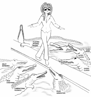
Conversion to an ASIC process can be stressful; there are hungry gators swimming in those waters! Some hazards to watch for include delay networks, race conditions, combinational feedback, pulse generators, floating internal busses, clock skew, and gated or divided clocks.
Most vendors offer a “turn-key” conversion process. In this design flow, the ASIC vendor takes complete responsibility for the conversion and provides all test vectors. This takes longer and is more expensive than a “joint-design” conversion, where the FPGA designer provides all or part of the test vectors and takes responsibility for the conversion.
Figure 9-1 Watch for those alligators!
AMI (American Microsystems, Inc.) offers a no-vector conversion; this is the most painless conversion for the FPGA designer who hates simulation. However, the designer must obey the following rules, which is nearly impossible:
• Altera, Xilinx, and Actel devices only.
• Single external master clock.
• No combinational feedback loops.
• No delay dependencies or pulse generators.
• Single external master set/reset signal.
SYNCHRONOUS DESIGN RULES
The first rule is to do a synchronous design. This is not always an easy rule to follow, but each clock added to a design should be carefully considered. Every clock domain, every signal that crosses a clock-domain boundary, and every asynchronous signal is a hazard unless dealt with exhaustively. If the purpose of a design is to convert from one clock domain to another (like a FIFO does), then, obviously, you have no choice. If you need to save power, but some of the design needs to run at high speed, then again you have no choice. My personal preference is to run a design at the lowest possible speed, because this reduces RFI emissions and makes the design more tolerant of the inefficiencies of a generic HDL implementation. If a section of the design must be asynchronous, put it in quarantine. Keep it segregated from the synchronous parts of the design and document it well so that the design intent and hazards are clear.
It’s not hard to handle asynchronous signals, but it is easy to forget to do this handling. The result is a design that works, but does not work reliably.
ASIC conversion vendors sometimes offer “vectorless” conversions if the design is 100% synchronous. This will reduce the span time for conversion and reduce cost. It also reduces stress on the FPGA designer because the test burden is removed. The ASIC vendor likes this, because the design is relatively trouble-free and the test vectors can be automatically generated. For the FPGA designer, creating a 100% synchronous design is almost impossible but is a very worthwhile goal.
Use Generic Logic Constructs
ASIC vendors who do FPGA conversions routinely replace RAM and other modules (like adders and counters) with parameterized modules selected from their library. However, each substitution contributes a new block to the design, and each change adds to the risk that something will go wrong. LogiBLOX or cores should be evaluated for ease of conversion or substitution before being used in the FPGA design. The netlist should be “untouched” as much as possible during the conversion process. If your design has nothing but NAND gates in it, it will convert painlessly, because no module substitution will occur.
In a gate array, your RAM and ROM modules will be replaced with registers. This results in an explosion of the gate count. For a 512-by-8 RAM module, 4,096 flipflops will be instantiated. The cell decoding logic adds to that number (decoding-logic complexity doubles for each added address line).
One feature that is particularly troublesome during ASIC conversion is RAM initialization (or ROM contents, the same thing). The FPGA can write data into RAM cells during the power-up configuration process. There is no corresponding magic configuration mode in the ASIC; all RAM cells must be written to via the RAM data bus.
Power-On Conditions
Part of the training wheels for an FPGA design is the power-up initialization of all I/O pins via the use of GSR (Global Set/Reset) resources and the device configuration process. An ASIC will not have these features unless the designer specifically puts them in. The ASIC vendor tends not to want to use many global networks (like reset and/or preset networks) because they must be custom routed and they consume routing channels.
Internal Busses
Xilinx and other FPGA vendors allow the use of internal tristate busses and buskeepers to prevent problems due to floating buffer inputs. Some ASIC vendors do not have this capability or prefer not to use the technology because it complicates testing. Exemplar Leonardo has a feature where internal tristate busses can be automatically converted to MUXes for technologies that don’t support internal tristate busses.
Configuration Pins
Often the FPGA configuration pins are used in external logic (for example, using the configuration CONF_DONE pin in a Power-On Reset logic). Special logic will have to be designed into the ASIC to provide configuration-pin emulation. The FPGA designer needs to define which signals are used and how the pins are expected to act. For common FPGA signals and architectures, the ASIC vendor will have some experience with these signals and will be able to assist.
Pin I/O Buffers
The input signal thresholds must be defined by the FPGA designer. Input threshold options include TTL (where the threshold voltage is about 30% of the supply rail), CMOS (where the voltage threshold is about 50% of the supply rail), or custom.
The output pin drive requirement must also be defined by the FPGA designer. The use of low-impedance (high-current) buffers should be minimized to reduce power consumption and RFI noise generated by the design. The ASIC process probably has more options for drive capacity than the FPGA. Always use the slowest and lowest-power pin buffer that will do the job.
OSCILLATORS
Oscillators are analog circuits, but sometimes oscillator buffers are available in FPGA technology. These are inverting buffers with low gain to help assure that the oscillator stays in the linear mode, the inverter provides 180 degrees of phase lag, and the RC (cheapest, sloppiest), ceramic resonator (cheap, but not too sloppy), or crystal (best performance, but more expensive) provides the remaining 180 degrees of phase lag to meet the requirement for oscillation (a closed loop with 360 degrees of phase shift and an overall gain of one). A typical gate oscillator is shown in Figure 9-2.
Figure 9-2 Typical Gate Oscillator Circuit

These circuits will need to be identified to the ASIC vendor to assure a compatible conversion. It’s likely that the oscillator will end up being gated or multiplexed (this is much different than having a gated clock as part of the normal operating mode) so that the test equipment can drive the clock output with a clock of known frequency and phase. This circuitry will be added as part of the ASIC design process and probably will not be part of the FPGA design.
Never strap an oscillator enable pin high or low; put a resistor in so that an external source can enable or disable the oscillator as shown in Figure 9-3.
Figure 9-3 ASIC Oscillator Disable Circuit

For best performance, clock circuits should be isolated from other noise sources by physical distance or by guard rings, and the wiring should be kept tight to reduce loop areas. Note: the oscillator inverter is run in the linear mode, and the output should approximate a sinewave as much as possible to reduce EMI.
DELAY LINES
The FPGA designer sometimes uses a delay line to create time-delayed signals, particularly when interfacing with external SRAM or DRAM components. This delay is another analog circuit, so use caution! The delay line might be a string of buffers. This method of creating a delay is not recommended, because it depends on typical buffer delays which are not controlled and which change with temperature and process/technology changes.
During ASIC conversion, delay-line buffers will be replaced with buffers with different propagation delays (usually shorter, because ASIC buffers are typically faster than FPGA buffers) or will be completely removed because they represent redundant logic from a digital point of view. These delays must be documented and verified to insure they get implemented properly.
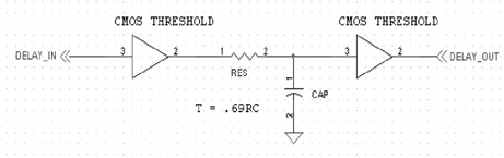
An option might be to use an external circuit to create the delay as shown in Figure 9-4. This circuit might be an RC delay with buffers to minimize the effect of changing the pin driver and pin loading during ASIC conversion. This delay is not precise and depends on the propagation delay of the pin drivers, the buffer propagation delays, the buffer threshold voltages, the tolerances of the RC components, operating temperature, and the ether-flux of the moon’s gravitational field.
Figure 9-4 Typical External Buffer RC Delay Circuit
Even better, a delay can be created from a serpentine circuit board trace with about 175 picoseconds of delay per inch as shown in Figure 9-5. Remember to include the buffer delays, the pad delays, and the circuit-board trace delays. There are many assumption in this delay, and your mileage will vary. The reader is urged to read Johnson and Graham’s High Speed Digital Design, a Handbook of Black Magic (see bibliography) before implementing a circuit like this.
Figure 9-5 Typical External Trace Delay Line Circuit
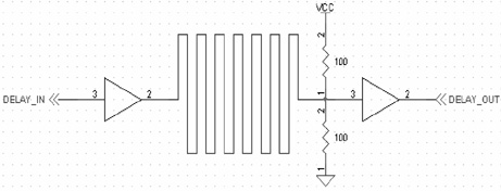
Assumptions include the use of FR-4 circuit-board material, 20-mil traces, 0.6 inches per segment, 50-mil segment pitch, and that you have a valid exemption from Murphy’s Law.
Even better yet, think about spending some money and using a digital delay circuit like those available from Dallas Semiconductor and others.
THE LANGUAGE OF TEST
We’re not going to cover test topics in depth, but we can learn a few buzzwords.
• At-speed testing. Testing performed at the actual operating speed of the design. Most testing is performed at slower clock speeds that are comfortable for the test equipment. These frequencies might be on the order of 1 to 5 MHz.
• Boundary scan. A test scheme where MUXes and latches are added to the design to support shifting serial data in and out. This allows test patterns to be applied and internal logic states to be read out.
• BIST. Built-In Self-Test, where hardware is added to the design to allow it to test itself.
• Fault grading. A measure of the how well the design hardware is tested. It is the ratio of the number of test vectors and the fault coverage.
• Functional test. Testing a device by applying user-provided test inputs and checking outputs. These tests are generally not very thorough. These are not parametric tests for AC performance.
• IDDQ Tests of power-supply current when all internal nodes are quiet. The only inputs are terminations to prevent oscillation and to keep gates from going linear. This is a quick test to reject devices that were manufactured improperly.
• JTAG. Joint Test Action Group that created the IEEE 1149.1 boundary scan register and test access port (TAP) standard.
• Observability. The ability for test equipment to access an internal node. All output pins are observable.
• Parametric testing. Testing for gate input thresholds and output drive capability. These are analog tests which verify the ASIC processes.
• Partial scan. A scan test that covers only selected parts of the design.
• Test coverage. A figure of merit for a test suite; it’s the ratio of all detected faults to the total number of possible faults.
• Stuck-at faults. A failure caused by a node staying in a zero or one state when it should be driven to a different state.
Boundary Scan
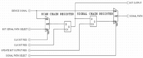
Because SRAM-based FPGA devices can be reprogrammed, the FPGA manufacturer can load a test configuration and do a thorough production test. Custom devices, like your ASIC, must have test support designed in. A common method of providing test support is to insert boundary scan logic (BST), which creates a serial chain that runs near the outside of the device under test. This chain can include other devices. The serial chain can be four or five signals (TDI, Test Data Input, TDO, Test Data Output, TCLK, Test Clock, TMS, Test Mode Select, and an optional Test Reset, TRSTn). Inside the ASIC, MUXes are inserted which allow selected signals to be connected to a long shift register; this allows signals to be shifted in and out of the device being tested.
BST adds hardware to the ASIC as shown in Figure 9-6, the added hardware increases the ASIC design by 15 to 25%. It also adds delays to signal paths on the order of 1-2 nsec for each BST MUX. Insertion of the BST hardware and generation of scan vectors are automated processes. Note that the device signal always flows through a MUX. This architecture allows the serial chain to read device signals, or to shift (pass-through) other test signals in the chain, or to pass test signals into the signal chain.
Figure 9-6 Boundary Scan Hardware Overhead
There are other test methods. A complete discussion of them is beyond the scope of this book, but we can at least list them and say a few words about them. Tests can be divided into production tests (where the design is validated and process problems are tested for), design conversion tests (insuring that the design was converted properly; this is usually done mostly with designer-supplied functional test vectors), and static timing tests (to assure that the ASIC’s different gate delays and clock skews don’t cause problems).
IDDQ Test This is a quick test for production problems; if the current drain of the device is much higher than expected, then a manufacturing defect has probably occurred and the device can be quickly rejected.
Functional Test This type of test uses test vectors provided by the designer which emulate typical operating modes and look for predicted outputs. This type of test is generally not very thorough, because the designer doesn’t think of all the various combinations of input modes and logic sequences.
ATPG (Automatic Test Vector Generation) These test vectors can include serial vectors (the ones that are clocked into the BST scan chain, if present) and parallel vectors (the ones presented in parallel to the device inputs).
PRINT-ON-CHANGE TEST VECTORS
The ASIC vendor will request print-on-change (POC) test vectors; this is an ASCII-formatted list of input sequences and expected output test patterns. Fortunately, it’s not difficult to extract these vectors from the Verilog test fixture using $display and $monitor directives.
From Listing 9-1, you can see that the delay through the gate is 3 nsec (the output changes in the period between 50 and 53 nsec).
Listing 9-1 Simple POC Vector Example, OR Gate
II O
NN U
12 T
TIME
0 00 0
50 01 0
53 01 1
100 00 1
103 00 0
150 10 0
153 10 1