
Previous chapters have explained the need for pulse width modulation (PWM), control of three-phase converters and presented some conventional methods that generate PWM on each phase independently. Some limitations in their practical implementation have stimulated efforts to find other principles to generate PWM controls. The most remarkable is the analysis of the three-phase inverter in the complex plane by the Vector Space theory. Understanding the mathematical representation of the inverter operation in the complex plane provided a tool for the generation of a new PWM algorithm called space vector modulation (SVM). (Note the difference between a vector space, which means a space of vectors, and a space vector, which means a vector with a spatial displacement.)
SVM has become a standard for medium- and high-power switching converters in both industry and university. The last 20 years have provided a large volume of publications that fully define SVM theory. Implementation on different digital platforms has been considered and some dedicated integrated circuits have already been developed on the basis of this principle. The SVM theory initially developed for three-phase voltage-source inverters has been extended with new applications to other three-phase topologies. Such methods will be presented in later chapters.
5.1 REVIEW OF SPACE VECTOR THEORY
5.1.1 HISTORY AND EVOLUTION OF the CONCEPT
The first vectorial representation of three-phase systems was introduced by Park [1], Kron [2], and Stanley [3]. They showed the separation of effects on two axes at the operation of a three-phase electrical drive. First, Park [4] replaced the variables associated to the stator windings with variables of fictitious windings rotating with the rotor. This work can be considered the base for the well-known theory of vector control or field-orientation control for induction and synchronous drives. In the late 1930s, Stanley [3] used the same idea for induction machine drives but he replaced the rotor variables to a frame fixed on the stator. During the 1960s, the advent of thyristors led to the systematic use of the space vector theory to analyze and control three-phase electrical drives. Kovacs and Racz [4] provided mathematical treatment along with a physical description and understanding of machine drive transients even in the cases in which machines were fed through electronic converters.
Space vector-derived methods were widely used by the industry in the early 1970s and numerous books have presented this theory. Stepina [5] and Serrano-Iribarnegaray [6] suggested the use of the space phasor to analyze electrical machines. The space phasor concept is now used mainly for current and flux measures when analyzing electrical machines.
It was again the semiconductor technology that pushed for more consideration of the vectorial analysis theory in the early 1980s. Development and intensive use of the first microprocessors in industry opened new research areas to find the most appropriate implementation algorithms for conventional issues of PWM generation, current control, or field-orientation-based control of electrical drives. Murai and Tsunehiro [7] reported in 1983 an improved PWM method derived from vectorial analysis of the operation of a three-phase inverter. A few years later, different researchers [8,9,10,11], considering all three phases in a unique vector, developed the SVM theory further to control the inverter in open loop and, later, in closed loop. The new method provided great advantages in digital implementation with the newly arrived microcontrollers.
5.1.2 THEORY: VECTORIAL TRANSFORMS AND ADVANTAGES
A three-phase system defined by ux(t), uy(t), and uz(t) can be represented uniquely by a rotating vector uS in the complex plane:
(5.1) |
where a_=ej⋅2π3 and a2_=ej4π3.
All vectors in the complex plane form a space of vectors [12]. The mathematical theory of vector spaces is next employed to provide an instrument for analysis.
A base within a vector space consists of a system of vectors b (b1,b2,b3) that is a unique representation of any member V of that vector space as a linear combination of vectors from b. For instance,
(5.2) |
or
(5.3) |
where vd, vq, and v0 are also called coordinates. If the vector space has a finite dimension, then all possible bases have the same number of elements. The dimension of a vector space refers to the number of vectors within any base. When applied to three-phase power systems or power converters, the dimension of the vector space is three, which means that any base has three elements. A base is ortho-normalized if all its vectors are unitary and any two different vectors are orthogonal. The mathematical theory of vector spaces also provides tools for making transformations between different bases of the same vector space. These transformations are unique and reversible and can have linear or rotational effects on the vectors.
All the previously reported papers in the three-phase power electronics indirectly consider the orthogonal base vectors as
(5.4) |
(5.5) |
(5.6) |
The selection of this set of vectors is not unique. Coefficients and functions within each term may have other forms depending on where they are to be applied.
In our case, in a three-phase system, we would like to take advantage of sin and cos functions because we know that our phase voltages have this type of variation and we hope to separate DC quantities (constant numbers) as coordinates of Equation 5.2. The discontinuous PWM algorithms presented in Chapter 3 can enlarge the field of application of this theory. The ON-time variation is represented by the discontinuous function, depending on the phase coordinates and the conventional outputs of the vector control algorithm. Selecting base vectors characterized by that type of variation would provide a mathematical instrument for directly transforming the quasi-DC quantities of the vector control algorithm into an ON-time variation function that can be used to control the PWM generator.
Another example can refer to the selection of the coefficients in [2]. Engineers analyzing power systems take advantage of this property by defining base vectors and transform coefficients from either power conservation or magnitude conservation constraints. Thus, the coefficient (3/2) from Equations 5.4 and 5.5 is calculated to preserve the magnitude of the vector in the complex plane, but some engineers use a coefficient of sqrt(3/2) to preserve power through the transform.
Basically, this theory says that we can decompose any vector in the complex plane in a form shown by Equation 5.2 where the base vectors may have a form as in Equations 5.4, 5.5, 5.6. The coordinate vd of Equation 5.2 is the result of that part of the first phase voltage that follows cos(ωit) added to that part of the second phase that follows cos(ωit− 2π/3) and to that part of the third phase that follows cos(ωit− 4π/3).
Similarly, the coordinate vq of Equation 5.2 is the result of that part of the first phase voltage that follows sin(ωit) added to that part of the second phase that follows sin(ωit − 2π/3) and to that part of the third phase that follows sin(ωit − 4π/3).
Finally, the quasi-DC components in all the phases are added in v0. Replacing Equations 5.4, 5.5, 5.6 in 5.2 yields a relationship between coordinates in different bases:
This is the core idea of a vector transformation from coordinates ux(t), uy(t), uz(t) to coordinates ud(t), uq(t), u0(t) or vice versa. This operation of transforming a three-phase system in a unique vector followed up by the transformation of the orthogonal vector coordinates in quasi-DC coordinates (d,q,0) is known as Park/Clarke transforms for three phase systems.
First let us transform the phase measures into orthogonal coordinates with a third homopolar (or zero sequence) coordinate. Any vector in the complex plane can be decomposed in two orthogonal coordinates (Uα, Uβ, U0) and a homopolar coordinate U0.
(5.8) |
where (Uα, Uβ) are forming an orthogonal two-phase system and us_=Uα+j⋅Uβ If the system of phase voltages is symmetrical, the homopolar term equals zero and it can miss within the previous transform. Moreover, this transform is unique as shown in Figure 5.1.
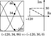
FIGURE 5.1 Derivation of a vector equivalent to a three-phase system.
This transform is not directly necessary for the presentation of space vector modulation algorithm, but is very used by electrical engineers in vector control of power converters. The two coordinates (α, β) are next transformed through a vector rotation with the rotational frequency identical to the electrical frequency.
(5.9) |
Frequently, these two transforms are used in a single transform stage that coincides with the vector space theory introduced in the beginning (5.7):
[UdUqU0]= 23 ⋅ [cos θcos [θ−2 . π3]cos [θ−4 . π3]sin θsin [θ−2 . π3]sin [θ−4 . π3]121212] ⋅ [uXuYuZ] |
(5.10) |
Each of these transforms has an inverse that allows transformation to the phase measures from the orthogonal coordinates. The general inverse transform is given by
{uX(t)=Re [us_]+u0(t)uY(t)=Re [a2_ ⋅ us_]+u0(t)uZ(t)=Re [a_ . us_]+u0(t) |
(5.11) |
where u0(t) = (1/3) · [uX(t) + uY(t) + uZ(t)] represents the homopolar component. Particular forms are also available for Park and Clarke inverse transforms.
5.1.3 APPLICATION TO THREE-PHASE CONTROL SYSTEMS
This mathematical representation of three-phase measures treats the analysis of the three-phase system as a whole, instead of considering equations for each phase individually. Many control methods for three-phase systems have been derived from this mathematical approach.
Electrical drives (induction machine or synchronous machine drives) are controlled by the so-called field-orientation principle (Figure 5.2a). The three-phase grid interfaces or AC/DC converters (Figure 5.2b) are nowadays seen as active filtering systems controlled by the instantaneous power components (p–q) theory. All these systems use PWM algorithms in the final control stage.

FIGURE 5.2 Examples of application of vectorial representation in control.
5.2 VECTORIAL ANALYSIS OF THE THREE-PHASE INVERTER
The three-phase inverter presented in Figure 5.3 is built of six insulated gate bipolar transistors (IGBTs), but it can be made with any other power-switching device, depending on the voltage and current ratings.
Figure 5.4 presents the appropriate output voltages without PWM. This is the so-called six-step operation and it is also the simplest and oldest control method for this type of power converter. Different switching states are given in the figure with a digital code (for example: 1 0 1), showing whether the high-side IGBT is ON (for 1) or the low-side device is ON (for 0). Another possible notation uses a sign to show where the pole terminals (A, B, C) are connected.
Each state of the power converter leads to a switching vector in the complex plane. There are thus six active switching vectors V1,…,V6 equally sharing six sectors within the complex plane (Figure 5.5).
The vectorial analysis of the operation of this system is first developed for an inductive three-phase load. Each phase current waveform can be derived by the integral of each phase voltage equation.
(5.12) |
Applying transform (5.2) to these allows writing the same equations for the vector space variables.
(5.13) |

FIGURE 5.3 Basic topology for the three-phase voltage-source inverter.
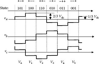
FIGURE 5.4 Output voltage waveforms and state coding for the six-step operation.
The variation slope of the phase current is doubled when the phase voltage gets doubled. The maximum value of the phase current is denoted here by IM. During the time interval [t1, t2], the output voltage vector is V1 and the phase voltages are 2/3 Vdc, −1/3 Vdc, and −1/3 Vdc.
Choosing the time origin in t1(t1 = 0), the load current and voltage expressions can be mathematically expressed as linear variations during the interval (t1, t2). From Figure 5.6, it yields:
{ia(t)=−0.5 ⋅ IM + 2 ⋅ Vdc3 ⋅ L ⋅ tib(t)=−0.5 ⋅ IM + Vdc3 ⋅ L ⋅ tic(t)=IM − Vdc3 ⋅ L ⋅ t |
(5.14) |
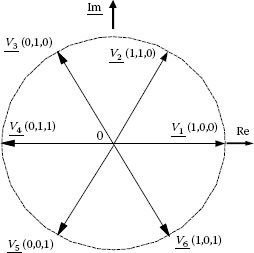
FIGURE 5.5 Switching vectors corresponding to the six-step operation of the inverter.
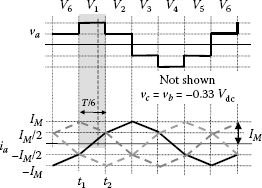
FIGURE 5.6 Output phase current and voltage waveforms: (a) calculation; (b) full-cycle trajectory.
Applying definition (5.1) to the space vectors associated to the current and voltage waveforms yields:
(5.15) |
(5.16) |
where
(5.17) |
leading to
(5.18) |
and
(5.19) |
It can be seen from Equation 5.18 that the magnitude of each voltage switching vector is (2/3)Vdc. The tip of the current space vector has a linear variation in the complex plane, with the Real part varying linearly from −0.5IM to 0.5IM during the time interval [t1, t2] of duration T/6 (Figure 5.7).
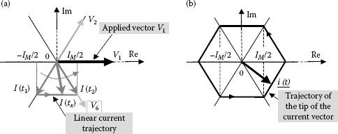
FIGURE 5.7 Current vector trajectory in the complex plane for a pure L load.
This trajectory is oriented so that the current space vector is quasi-perpendicular on the voltage space vector and this was expected from the integral form of the inductive load equation. The vector projection on the Real axis represents the value of the first phase current. Considering the variation of the phase current during the interval [t1, t2] allows determination of the maximum value of the current (IM). It yields:
(5.20) |
(5.21) |
The voltage space vector is identical with the switching vector V2 at the next interval. The current space vector moves between the position along the vectors V6 (at t2) and V1 (at next interval, t3). Similar calculation proves the linearity of this trajectory. Extending the same reasoning for all six possible voltage-switching vectors defines the trajectory of the tip of the current vector in the complex plane.
The resulting trajectory is a hexagon oriented along the voltage-switching vectors.
The projection on the real axis is at any time equal to the current on the first phase. Currents or voltages on the other two phases can be graphically derived by the projection on two fictitious axes at 120° and 240°, respectively. This vectorial analysis provides information about all the currents and voltages in the system. Moreover, because of the 60° symmetry of the operation, it is enough to limit the vectorial analysis to a 60° sector.
Extending this analysis to the general case of an R–L load (Figure 5.8), consider the vectorial equation for the load circuit

FIGURE 5.8 Current vector trajectory in the complex plane for an R–L load.
(5.22) |
with the generic solution
(5.23) |
where C is a complex constant and τ = (R/L) represents the time constant of the load. In other words, for each switching vector applied to the load, the current trajectory is a portion of exponential. To better define such trajectory, let us suppose the initial value as being equal to i(0) = I and the final value after T/6 is
i_[2 ⋅ π6 ⋅ ω]=I ⋅ e−jπ3
These conditions help defining the constant C and initial value I:
Replacing complex constant C in Equation 5.23 yields:
(5.25) |
5.2.2 DEFINITION OF FLUX OF a (VOLTAGE) VECTOR AND IDEAL FLUX TRAJECTORY
Three-phase power-switching inverters are often used to supply a machine drive or a strongly inductive load. The leakage inductance of the machine and the inertia of the mechanical system account for low-pass filtering of the harmonics provided by the discontinuous power flow at switching. If a voltage drop across the resistance and leakage inductance of the stator windings is neglected, the flux linkage in the machine is approximately equal to the time integral of the impressed voltage. The flux vector yields
(5.26) |
A very similar definition can be made for AC/DC applications, where the boost input inductance accounts for low-pass filtering of the voltage pulses resulting from the PWM operation of the power stage.
All these applications will work properly if the magnitude of the flux linkage is kept constant, which denotes a circular trajectory of the flux. As Vs occupies different discrete positions in the complex plane, its time integral leads to a polygon close to a circle, as anticipated by Figure 5.9. What was not explained previously is the existence of zero vectors in the flux trajectory at control with PWM. A zero vector, also called homopolar vector, is achieved when all power devices are connected to the same DC bus terminal, positive or negative. Any of the PWM methods explained previously in Chapter 3 uses zero-vector states during operation. Voltages applied on each phase of the load equal zero in this case and the integral of these voltages show no displacement of the flux trajectory. A direct consequence of this is the possibility of using zero vectors to regulate the speed of the flux trajectory (Figure 5.10).
A real trajectory of the flux achieved by PWM operation presents both radial and angular errors. The radial errors are variations along the radius of the circular locus, whereas the angular errors are variations from a constant rotational speed. In a motor drive, any error in the flux trajectory has a direct influence on the torque ripple. The difference between the reference λ0 having a circular locus in the complex plane and the actual trajectory λ produced by a PWM inverter causes the torque oscillations.
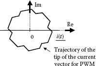
FIGURE 5.9 Current space vector trajectory for a simplified PWM case.

FIGURE 5.10 Flux trajectory improved by increasing the switching frequency even if the same shape of pulses is used.
The dependence of the torque pulsation on radial and angular components of the flux error has been analyzed and presented in [13,14,15,16,17], and it has been stated that the torque oscillation is more sensitive to the angular error than the radial error. The angular error can be reduced by operating with a smoother rotational speed that can be achieved when employing more zero states on the flux locus. The radial errors can be reduced with an optimal polygonal flux locus having all edges staying as close to the desired circular locus.
As the angular error is more important than the radial error, the torque ripple is lower when a higher carrier frequency (more zero vector states) is employed, even though this splits a polygonal flux locus to a reduced number of edges. A limited switching frequency is desired for completely different reasons, such as reduction of the switching loss.
5.3 SVM THEORY: DERIVATION OF TIME INTERVALS ASSOCIATED TO ACTIVE AND ZERO STATES BY AVERAGING
SVM was developed in [7,8,9,10,11] and the importance of this method has been outlined in many publications [18,19,20,21]. The three-phase inverter presented in Figure 5.3 produces a symmetrical three-phase system of voltages on the load. If the magnitude of the phase voltages is Vs, this is equivalent to generating a circular locus with a constant radius equaling the same magnitude. Such an ideal locus cannot be achieved with a switching power converter that leads to six discrete positions of only the voltage space vector. Each desired position on the circular locus can be synthesized only through an average relationship between two neighboring active vectors and zero vectors
(5.27) |
where Ts is the sampling period of the given circular locus (as, usually, the switching frequency is not equal to the carrier frequency, it is preferable to call Ts the sampling period) and ta, tb are the time intervals allocated to the neighboring vectors Va, Vb. The averaging process is a result of the low pass filtering action of the load on the voltage pulses. Zero vectors are necessary to keep the sampling interval constant and they are calculated by
(5.28) |
In order to calculate the time intervals associated with a desired position of the voltage vector in the complex plane, the symmetry after a 60° interval is first noticed. This opens up the possibility that the analysis can be limited to a generalized sector of 60°, repeated six times. To simplify the calculation, such a sector is considered superimposed with the first sector of the complex plane.
Decomposition of Equation 5.27 on both Real (Re in all figures) and Imaginary (Im in all figures) axes yields:
{Re:Vs⋅cos α⋅Ts=(23⋅Vdc)⋅ta+(23⋅Vdc)⋅12⋅tbIm:Vs⋅sin α⋅Ts=(23⋅Vdc)⋅√32⋅tb |
(5.29) |
Time intervals involved in the PWM generation are calculated by (Figure 5.14):
(5.30) |
Calculation of the time intervals associated with each active state is only the first part of the generation of a PWM algorithm. Determination of the switching sequence is the second stage. Modern microcontrollers achieve both functions and take advantage of special expressions for the time intervals associated with the conduction of each switch. These allow the implementation of the SVM method within the center aligned PWM hardware. Calculation of the pulse widths is based on a memory lookup table for the sine function within a 60° interval or of the sinα and sin(60 − α) functions within a 30° interval. Alternative solutions are based on real-time interpolation of a minimized look-up table. This interpolation can be carried out by fuzzy logic as well [22,23]. Chapter 8 will present hardware solutions available in the market to implement SVM.
Observing Equation 5.30 and Figure 5.11, one can derive the maximum modulation. It will correspond to the circular locus with the maximum radius and it equals:
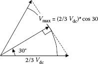
FIGURE 5.11 Definition of the maximum modulation index. (From Neacsu, D.O. Tutorial presented at IECON’01: The 27th Annual Conference of the IEEE Industrial Electronics Society 2001, IEEE Paper 0-7803-7108-9/01. © (2001) With permission of IEEE.)
(5.31) |
This value is 15% higher than the maximum modulation index from the sinusoidal modulation.
The sampling period Ts is shown in Equation 5.30. Note the nomenclature difference between sampling interval/sampling frequency and switching interval/switching frequency. A new PWM method can be derived by changing the sampling frequency while using the same equations. The frequency modulation is the result of adjusting Ts during the fundamental or cycle period [10,17]. Several methods have been developed by using the sampling frequency as a degree of freedom in optimization after one or more criteria: low harmonics reduction, harmonic current factor (HCF) reduction, and so on, but all redefine Ts as
(5.32) |
with N being number of intervals over the fundamental period (at frequency f).
Conventional PWM is characterized by δ = 0, while the optimized methods require Ts modulated so that it gets shorter periods at 0 and 60° but lengthier at 30° within each 60° sector. These ensure minimum angular errors, current distortion factor at low harmonics, and minimum torque oscillations. Random SVM represents a special type of frequency modulation.
Finally, note that the averaging principle used here does not provide any requirement on zero vector generation during t0. Moreover, the sequence of the active and zero vectors within the sampling period is not unique and these degrees of freedom make the difference between space vector methods. The most well-known alternatives will be analyzed later in this chapter.
5.4 ADAPTIVE SVM: DC RIPPLE COMPENSATION
The presence of the DC voltage (VDC) in Equation 5.30 compensates for the ripple of the DC bus voltage [24] (Figure 5.12). This ripple can be produced with insufficient filtering of the input rectifier power stage in a back-to-back converter structure.
Measuring the DC voltage at each sampling interval or with a larger sampling period will be appropriately compensated by Equation 5.30 for the effect of this ripple in the output voltage.
Figure 5.12 shows how the time intervals ta, tb are affected by the variation of the DC bus voltage in order to preserve the same harmonics on the load. The drawback of this method is that it reduces the maximum available voltage at the inverter output. The maximum available output voltage is achieved when the DC bus has the lower value within the ripple and the inverter operates at maximum modulation index of 0.866.

FIGURE 5.12 Reduction of the maximum output voltage by unfiltered DC bus with 6-step rectifier (V represents the grid side RMS voltage).
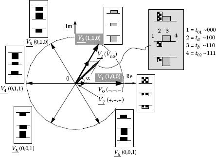
FIGURE 5.13 Generation of voltage space vector by SVM. (From Neacsu, D.O. Tutorial presented at IECON’01: The 27th Annual Conference of the IEEE Industrial Electronics Society 2001, IEEE Paper 0-7803-7108-9/01. © (2001) With permission of IEEE.)
This SVM algorithm calculates the time intervals associated with each state based on the polar coordinates (Vs, α) of the desired space vector position. This is not very convenient for vector control methods for drives and for active filtering.
The result of the vector control methods is given in the coordinates (vx, vy) and these can also be expressed depending upon the polar coordinates (Equations 5.33, 5.34, 5.35, 5.36, 5.37, 5.38) [25].
Sector 1
(5.33) |
Sector 2
(5.34) |
Sector 3
(5.35) |
Sector 4
(5.36) |
Sector 5
(5.37) |
Sector 6
(5.38) |
For the first sector, replacing Equation 5.33 in 5.30 yields:
(5.39) |
For the second sector:
(5.40) |
Similar calculus leads to the following results [25]:
Sector 1
(5.41) |
Sector 2
(5.42) |
Sector 3
(5.43) |
Sector 4
(5.44) |
Sector 5
(5.45) |
Sector 6
(5.46) |
The time intervals allocated to the zero vectors remain
(5.47) |
Another mathematical form for the transformation of (vx, vy) coordinates into time intervals is provided by Equation 5.48 and is derived from (x, y)-type orthogonal coordinates of the active switching vectors denoted here as and . The relationship for the time intervals yields:
(5.48) |
Any of these forms expressing the time intervals represents only the first step for PWM implementation. Next, the time intervals corresponding to the inverter switching states need to be converted into a logical switching sequence applied to the gates of IGBTs. In order to implement this step, the switching reference function (also called modulation function) is defined.
5.6 DEFINITION OF SWITCHING REFERENCE FUNCTION
Once we know the time intervals for each state, we need to establish the sequence of these intervals. If we try to directly use the previous relationships, the definition of the switching sequence can be implemented only by the software. It is more advantageous to define a function called the switching reference function that represents the duty ratio of each inverter leg or the conduction time normalized to the sampling period for a given switch; this is a mathematical function varying between 0 and 1 centered around 0.5. This is also called the modulation function.
The switching reference function can be derived by algebraic operations between the time intervals previously calculated. For instance, on the first sector from Figure 5.13:
• The instant when S1 goes ON equals t01 from the beginning of the sampling period, and the value of the switching reference function for S1 will equal [t01/Ts].
• The instant when S3 goes ON equals a delay of t01 + ta from the beginning of the sampling period, and the value of the switching reference function for S3 will equal [t01 + ta/Ts].
FIGURE 5.14 Space vector modulation with adaptive compensation.
• The instant when S5 goes ON equals a delay of t01 + ta + tb from the beginning of the sampling period, and the value of the switching reference function for S5 will equal [t01 + ta/Ts].
The switching reference function is calculated at the sampling instants, and the real variation is a staircase waveform that can be interpolated as shown in Figure 5.14. The switching reference function has the same meaning as the reference used in sine-triangle comparison-based PWM methods. It is, therefore, simpler to use the mathematical definition of a continuous function not influenced by the sampling frequency rate. At this point, it is also easier to understand why the repetitive frequency used in PWM generation is called sampling frequency. It simply means to sample the switching reference function.
After successive derivations from Equations 5.38, 5.39, 5.40, 5.41, 5.42, 5.43, one can calculate the switching reference function for all sectors. This is shown in Figure 5.15 for the case of regular SVM. The difference between this function and a pure cosine function is given by the following equation with a rich content in the third harmonic:
(5.49) |
The third harmonic is present in the switching reference function but it is not present in the output phase or line voltages. It only represents the average of the A–M voltage from Figure 5.16.
(5.50) |

FIGURE 5.15 Switching reference function for the regular SVM. (From Neacsu, D.O. Tutorial presented at IECON’01: The 27th Annual Conference of the IEEE Industrial Electronics Society 2001, IEEE Paper 0-7803-7108-9/01. © (2001) With permission of IEEE.)

FIGURE 5.16 Third harmonics in the SVM generation.
The previous chapter showed the role and meaning of the injection of the third harmonics in the sinusoidal modulation. The amount of this harmonic injection has been shown to vary depending on the optimization objective:
• Maximization of the fundamental content (third harmonic with 0.25 of the magnitude of the sinusoidal reference)
• Minimization of the total content in harmonics (third harmonic with 0.16 of the magnitude of the sinusoidal reference)
The third harmonic in the SVM method is between the two values previously calculated at about 0.22. References [26,27,28,29,30] analyze the equivalence between regular, sampled sine-triangle methods and SVM and conclude that both methods are analogous and that conventional digital center-aligned PWM devices can be used for the implementation of the SVM algorithm.
5.7 DEFINITION OF SWITCHING SEQUENCE
5.7.1 CONTINUOUS REFERENCE FUNCTION: DIFFERENT METHODS
The number of switchings can be reduced with a special arrangement of the switching sequence so that only one switching on each inverter leg occurs during the transition from one state to the next. When using both available zero states from Figure 5.13, one zero state will start the sequence and the other will end it. For instance, the switching state sequence has to be _ _ _0 1 2 7 2 1 0_ _ _. The only remaining degree of freedom consists in the amount t0 shared between the vectors V0 and V7.
The averaging theory used for SVM calculation does not define a way of sharing t0 among the possible zero vector states. In the original method, t0 was shared equally between the two zero vectors. But this is not the most optimal partition solution. The same low-sampling frequency algorithm is analyzed but with different sharing of the zero states. All the sectors and bisectrix symmetries are considered as well as the alternation of the zero-state vectors. Results for the sharing ratio are shown in Figures 5.17 and 5.18 for a low number (equal to 24) of sampling intervals in the fundamental [31,32]. At larger sampling frequencies, the differences are smaller.

FIGURE 5.17 Effect of different sharing of the zero-states interval in content of fundamental (z). (From Neacsu, D.O. Tutorial presented at IECON’01: The 27th Annual Conference of the IEEE Industrial Electronics Society 2001, IEEE Paper 0-7803-7108-9/01. © (2001) With permission of IEEE.)
These results also show that high-performance SVM systems can be improved further by a different placement of the zero states within the sampling interval.
The two extreme situations for the sharing of the zero-state intervals are:
• Method D-I-H (direct-inverse-half) (Figure 5.19): Equal sharing of the zero vector intervals at each sampling interval (t0 = t7) [10,11] is shown in Figure 5.19 with a phase voltage waveform. Observe the trajectory of the tip of the current vector derived from this sequence.
• Method D-I-O (direct-inverse-one) (Figure 5.20): Use of only a zero-vector interval within each sampling period (e.g., t0 = 0, t7 = Ts − ta − tb).
• Both methods determine three switching on each sampling periods. Method D-I-O is often employed at high sampling frequencies, whereas in low frequencies, it produces even harmonics in the output phase voltage, as the waveform symmetries are no longer taken into account. The spectral differences between the voltages carried out by either Method D-I-H or Method D-I-O are small if the sampling frequency is large enough (Figure 5.21).
FIGURE 5.18 Effect of different sharing of the zero-states interval in HCF. (From Neacsu, D.O. 2001. Tutorial presented at IECON’01: The 27th Annual Conference of the IEEE Industrial Electronics Society 2001, IEEE Paper 0-7803-7108-9/01. © (2001) With permission of IEEE.)
FIGURE 5.19 Pulse generation with method D-I-H.
• Simple direct SVM or S-D-H method: The simplest way to synthesize the output voltage vector is to turn on all the switches connected to the same DC link potential at the beginning of the switching cycle (sampling period) and to turn them off sequentially during the sampling interval. The zero-vector interval splits between V0 and V7 (t0 = t7). The drawback consists in switching all three inverter legs somewhere in the middle of the sampling interval in order to change from V0 and V7 (for instance, the switch sequence: … 0127–0127–0127…). This method is similar to the usual sine-triangle comparison-based PWM (Figure 5.22).
• Symmetrically generated SVM: This modulation scheme is based on a symmetrical sequence within each sampling period. The phase voltages and switching signals are similar to the D-I-H method but the direct-inverse sequence is now inside the same sampling period (Figure 5.23). This method is similar to the center-aligned PWM devices and can be directly implemented in the existing PWM IC working on this basis.
Let us note here a very important difference between the Symmetrically Generated SVM and any of the other PWM algorithms described above. The use of the direct-inverse sequence produces harmonics at half the actual pulse frequency. This means that the spectra are equivalent with that of center-aligned PWM which is measuring the sampling interval from the zero state to another zero state of the same type. Figure 5.24a presents spectra for a normal PWM generation, while Figure 5.24b for a PWM with direct-inverse sequence of pulses. We can thus see the appearance of higher harmonics at half the pulse frequency. It means that there is a price to pay for the reduced count of switching instants. Figure 5.25 repeats the test for PWM with a pulse ratio of 48. It is therefore concluded that this type of PWM is better referred to as center-aligned PWM rather than quoting the two pulse sequence of direct-inverse.

FIGURE 5.20 Pulse generation with method D-I-O.
FIGURE 5.21 Three-phase voltage waveforms for (a) direct-inverse and (b) direct sequences at a low sampling frequency.
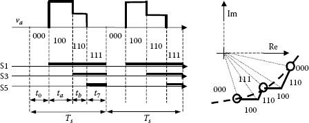
FIGURE 5.22 Pulse generation with Method S-D-H.
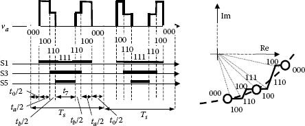
FIGURE 5.23 Pulse generation with Method S-G-S.
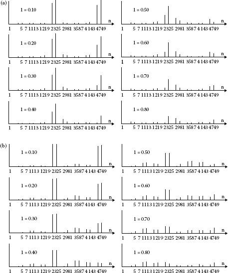
FIGURE 5.24 Harmonic results for PWM with a pulse ratio of 24.

FIGURE 5.25 Spectra for PWM with a pulse ratio of 48.
5.7.2 DISCONTINUOUS REFERENCE FUNCTION FOR REDUCED SWITCHING LOSS
The previous chapter including the regular sampled PWM algorithms, demonstrated the advantages of discontinuous algorithms to reduce the inverter switching loss [33,34,35,36,37]. The same idea is now used with the SVM algorithm as support [38,39,40,41,42].
The averaging theory used for SVM calculation does not define the sequence of the switching states. Any possible sequence of states will satisfy the average relationship if the time intervals are calculated correctly. Any two neighboring vectors are different by only one switching in an inverter leg. Therefore, always select the zero vector that does not change the status of that zero vector. For instance, in the first sector, shown in Figure 5.13, the first leg does not switch when active vectors are changed (from 1 0 0 to 1 1 0 or vice versa). Selection of the homopolar vector is not unique; each time two zero vectors can be used. Always selecting 1 1 1 as the zero vector means that the first leg will not switch for the whole first sector (for instance, sequences …–1 1 1–1 1 0–1 0 0–1 1 1–1 1 0–1 0 0–1 1 1–…). But this solution is not unique. In the first sector, the third leg does not switch when the active vectors are changed. This time, the lower switch will be ON during both active states (from 1 0 0 to 1 1 0 or vice versa). Always selecting 0 0 0 as the zero vector means that the third leg will not switch for the whole first sector (for instance, sequences …–0 0 0–1 0 0–1 1 0–0 0 0–1 0 0–1 1 0–0 0 0…). The advantage of using any one of these solutions is the reduction in switching losses. There are two solutions to minimize the number of switching processes within each sector of the complex plane. This raises the question whether to change or not the selection of the zero vector and the whole optimized sequence when passing to the next sector.
If we do not ever change the selection of the zero vector and always select the zero vector as 0 0 0 or 1 1 1, we get one of the following solutions:
• Method DZ0: The null vector is always fixed as [0 0 0]
• Method DZ1: The null vector is always fixed as [1 1 1]
The switching reference function can be calculated as shown previously in Section 5.5 and it leads to the waveforms shown in Figure 5.26, with large intervals that have no switchings for each of the six IGBTs within the inverter. These functions are also not linear.
As can be seen, the switch that is not switched is either always on the low-side (for the selection of the 0 0 0 zero vector) or on the high-side (for the selection of the 1 1 1 zero vector). Three switches are ON for extended periods of time and this may create a problem in inverter bridges that use isolation circuits such as the bootstrap or charge pumps for their gate drivers. That is why these methods are not used in the industry.

FIGURE 5.26 Switching reference function calculated for PWM generation with Methods DZ0 and DZ1.
To obtain a symmetrical stress from the power devices, the degree of freedom consists in alternating the zero vector at each 60° interval. As each phase can be kept unswitched for 120° consecutively, there is a degree of freedom in selecting where exactly the zero vector can be changed for sequences of 60°. For instance, the first leg can be kept unswitched from −60° to 60° (notice vectors 1 1 0 and 1 0 0 in Sector 1; 1 0 0 and 1 0 1 in Sector 6), but a 60° interval has to be chosen within this. Switching loss is approximately proportional to the magnitude of the current being switched and it would be better to avoid switching the inverter leg with the highest instantaneous current. In other words, the no-switching 60° interval can be selected at exactly the peak of the current.
How is the switching sequence selected? It can be based on four states in each sampling interval: a zero vector in the beginning, the first active state, the second active state, and another zero state at the end. Applying the principles explained earlier to such a switching sequence leads to results shown in Figure 5.27. The same phase voltages are obtained as in the case of Method S-D-H.
However, such a sequence violates the idea of having only one switch at a time and leads to four switches over a sampling interval. Another solution that respects this constraint and also takes advantage of the no-switch rule for 60° consecutively is different from conventional SVM. It uses a direct-inverse sequence:
|VA1 – VA2 – VZ | VZ – VA2 – VA1 | VA1 – VA2 – VZ | (Figure 5.28)
This selection of the switching sequence allows the maximum reduction of the number of switches.
There are several solutions accepted by the industry:
• Method DD1: The intervals of no switches coincide with the plane sectors. A null vector [1 1 1] is assigned for sectors 1, 3, and 5 and a null vector [0 0 0] is assigned for sectors 2, 4, and 6. The 60° interval without switches occurs right after the peak of the phase voltage. Generally, the current lags behind the phase voltage and the peak of the current fundamental settles in the next 60° after the peak voltage (Figure 5.29).
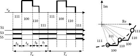
FIGURE 5.27 Switching sequence with four states taking advantage of no-switch rule on the first leg.

FIGURE 5.28 Modified space vector modulation.
• Method DD2: The 60° no-switch interval is spread equally around the peak of the fundamental of voltage. This method is very useful to reduce switching losses in grid-related applications, in which the power factor is unity and the peak of current is close to the peak of voltage (Figure 5.29).
• Method DD3: The 60° interval without switches can be spread equally around the measured peak of the phase current. Despite the difficulty of sensing the phase currents, this solution seems attractive, as it tracks the maximum loss reduction. However, if the phase current and voltage out of phase are greater than 30°, the 60° no-switch region will overcome the vector sector (Figure 5.30).
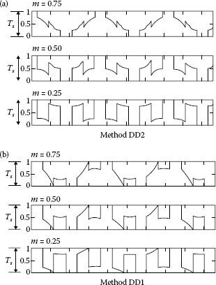
FIGURE 5.29 Pulse generation with methods DD1 and DD2 for different modulation indices.
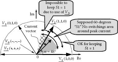
FIGURE 5.30 Vectorial discussion around the DD3 method. (From Neacsu, D.O. 2001. Tutorial presented at IECON’01: The 27th Annual Conference of the IEEE Industrial Electronics Society 2001, IEEE Paper 0-7803-7108-9/01. With permission.)
If the voltage vector is, for instance, V1 and the current vector is at 48°, equally spreading the no-switch region for the first inverter leg around the current vector leads to an area between 18° and 78°. For α > 60°, keeping the first phase ON (1) is no longer possible as the Sector 2 is characterized by switches in the first phase due to the use of V3 (0 1 0). There need not be any switches in the other two phases, but the other currents are less able to control the complexity, thereby compromising the merits of the method.
Let us analyze Figure 5.31 to understand how much power loss can be saved by using discontinuous PWM algorithms. Switching power loss for the discontinuous PWM algorithm is normalized to the switching power loss for the continuous PWM algorithm and shown in respect with the load power angle. The results are based on a computer-based analysis, considering the level of the load current at switching instant and the number of switching processes. The best case leads to 50% savings in switching loss [42,43,44].
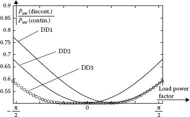
FIGURE 5.31 Switching loss for discontinuous PWM normalized to the switching loss for continuous PWM algorithm versus load power angle. (From Neacsu, D.O. The 27th Annual Conference of the IEEE Industrial Electronics Society 2001, IEEE Paper 0-7803-7108-9/01. © (2001) Printed with permission of IEEE.)
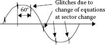
FIGURE 5.32 Output phase current when applying discontinuous PWM algorithms.
This reduction in switching loss does not exactly come free. There is a small drawback as the discontinuous PWM methods can introduce oscillations around the points where the sector is changed. This is due to the different set of equations used within each sector to calculate the time intervals. The effects are clearer at low output fundamental frequencies and they result in increased loss in the load and may introduce instabilities of the feedback control system (Figure 5.32).
5.8 COMPARISON BETWEEN DIFFERENT VECTORIAL PWM
The difference between the conduction loss among the SVM techniques is less than 3% of the total loss. Switching performance is presented in Table 5.1.
5.8.2 COMPARISON OF TOTAL HARMONIC DISTORTION/HCF
As shown in the previous chapter, the most important performance index for a power converter refers to the harmonic content in the output (input) current. This can be expressed by
TABLE 5.1
Switching Performance
Method |
No. of Switchings within Ts |
THDv |
No. of Switching States |
Direct–Inverse (DIH) |
3 |
4 |
|
Direct Inverse (DIO) |
3 |
3 |
|
Simple direct (SDH) |
6 |
4 |
|
Symmetric gen. (SGS) |
6 |
Least |
7 |
Direct–direct/000 (DZ0) |
4 |
3 |
|
Direct–direct/111 (DZ1) |
4 |
3 |
|
Direct–direct/sect (DD1) |
4/2 |
3 |
|
Direct–direct/peak (DD2) |
4/2 |
3 |
|
Direct–direct/mes (DD3) |
4/2 |
3 |
(5.51) |
and represents a normalization of the harmonic content to the fundamental.
These PWM algorithms have different sequences during the sampling interval and the number of switching processes is different. For this reason, the definition of the switching frequency differs from method to method. A proper comparison must consider the same switching frequency even if reached by different means.
The best harmonic content is achieved for reduced loss algorithm operated at high-modulation indices. In low-modulation indices, the best harmonic content can be achieved from the conventional SVM. The approximate threshold for this kind of comparison lies at a modulation index of about 0.6.
Many other researchers or engineers present the current harmonic by normalization to the harmonics obtained by a six-step operation at the power stage. Figure 5.33 shows the difference between harmonics with an inverter obtained by a six-step operation and a PWM inverter. The operation with six pulses introduces larger harmonics at low frequency (Figure 5.34).
By normalization to this waveform, the monotony of the plots changes. Results for the most well-known methods derived from SVM are shown in Figure 5.35.
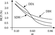
FIGURE 5.33 HCF for several modulation methods calculated for f1 = 50 Hz, fsw = 3.6 kHz.
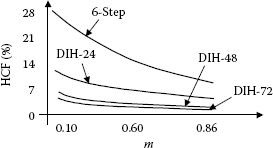
FIGURE 5.34 HCF for different number of sampling intervals over the fundamental.
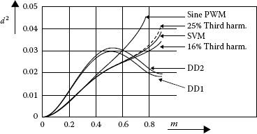
FIGURE 5.35 Distortion factor versus modulation index. (From Neacsu, D.O. Tutorial presented at IECON’01: The 27th Annual Conference of the IEEE Industrial Electronics Society 2001, IEEE Paper 0-7803-7108-9/01. © (2001) With permission of IEEE.)
It has been shown that the maximum modulation index of the regular SVM algorithm is achieved when the circular trajectory with the largest radius becomes tangential to the external hexagon formed with the switching vectors (see Figure 5. 11). The linearity of the PWM ends at this point.
Many applications, however, require more voltage up to the six-step mode. Operation between these two limits is called overmodulation and was presented in Chapter 4. Let us see here how an overmodulation algorithm can be defined under SVM.
First, the operation is characterized by a trajectory of the averaged space vector along a circle of radius m > 0.866 as long as the circle arc is located within the hexagon and along the hexagon sides in the remaining portions. The same equations 5.30 are used for PWM generation when the tip of the averaged space vector is on the circular trajectory. For points that lie on the sides of the hexagon, there is no zero state (t0 = 0) and the following equations are used for the active states:
(5.52) |
At m = 0.952, the trajectory shows at the hexagon, and no portions move into the circular locus. In order to advance toward the six-step operation, Operation Mode II is defined. This time, the velocity of the tip of the averaged space vector is controlled. The higher the modulation index is expected to be, the higher is the velocity in the center of each hexagon side and the lower in the corners. This mode converges smoothly into a six-step operation when the trajectory is limited to six discrete positions in the complex plane. The structure of a pulse over each sampling interval is composed of only two active states. Zero states are never used.
Both operation modes are characterized by nonlinear transfer characteristics with addition of harmonics that jeopardize the harmonic performance. This is natural because the six-step operation has been already shown to have important harmonics.
5.10 VOLT-PER-HERTZ CONTROL OF PWM INVERTERS
Chapter 4 introduced the volt-per-hertz control associated with PWM techniques. It has also been shown that industry uses PWM with different numbers of pulses for different fundamental frequency intervals (Figure 5.36). A larger frequency ratio is therefore considered for low frequencies, whereas the power converter operates at high fundamental frequencies with a smaller frequency ratio. Extension of this method to SVM control is presented next.
SVM control of a gate turn-off (GTO) inverter with a switching frequency below 960 Hz is shown in Figure 5.36 [45]. The switching frequency is limited to GTO devices and has wide enough pulses to compensate for the voltage drop across the stator resistance. The following operation modes are accordingly obtained:
• At higher frequencies: An operation mode with a constant voltage is preferred in order not to exceed the induction machine nominal value. The voltage is kept constant between 40 and 80 Hz with an optimal SVM having 24 pulses.
• At lower frequencies: A PWM method is used with V1/f = constant and a number of pulses on different frequency intervals: 24 pulses,… 20–40 Hz; 48 pulses,… 10–20 Hz; 96 pulses,… 5–10 Hz; 192 pulses,… <5 Hz.
The specifics of SVM for each operation mode are presented in Figure 5.37.
5.10.1 LOW-FREQUENCY OPERATION MODE
The relation V1/f = constant can be written as V1QTs = constant, where Q is the number of pulses over the fundamental period (also called frequency ratio). For each frequency interval shown in Figure 5.36, the magnitude and RMS of the output phase voltage take values within a finite interval and the vectorial representation of this operation brings us inside a circular corona (for example, between Vs1 and Vs2 in Figure 5.38).
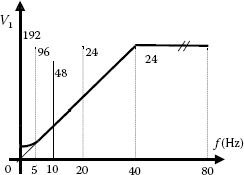
FIGURE 5.36 Volt-per-Hertz control.
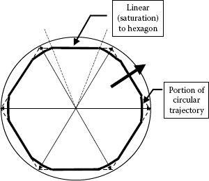
FIGURE 5.37 Operation modes.
The time allocated to the switching vectors neighboring a desired space vector position has been defined previously by Equation 5.30. These equations can be seen as ta, tb = constant Vs* Ts for a given direction on the complex plane. The similarity between these forms of Equation 5.30 and the volt-per-hertz control condition (V1QTs = constant) implies a possible modification of the RMS value of the output voltage by adjusting the sampling interval Ts while both ta, tb are kept constant (Figure 5.39).
In order to decrease the frequency, the sampling period is increased by enlarging the zero-states’ intervals. When the period doubles, the transition to the next domain occurs. This domain will be characterized by twice the number of pulses achieved by splitting the previous sampling period into two intervals. The use of the same time constants in all low-frequency operation modes is therefore possible, improving microcontroller and memory look-up table use. Figure 5.40 presents all possible positions of the tip of the space vector with the magnitude equaling the condition for transition from one domain to the next. Intermediary magnitude values are easily generated on the basis of the same time constants by enlarging the zero state intervals. This figure is also important as it shows the positions that need to have time constants stored in memory. All the other positions will use the same time constants (ta, tb). Considering all other symmetries of a three-phase system limits the total number of memory locations to

FIGURE 5.38 Circular corona.
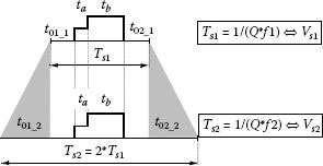
FIGURE 5.39 Pulse width changes over a circular corona in the complex plane.
(5.53) |
5.10.2 HIGH-FREQUENCY OPERATION MODE
The operation of the induction machine in high fundamental-frequency range implies limitation of the voltage [46]. The same PWM pattern is supposed to be used for all these frequencies. Due to the nature of the high-frequency operation, the number of pulses in this pattern is limited (24 pulses in our example) and the harmonic results are not very good. It is a good practice to define an optimal PWM algorithm on the basis of harmonic elimination or global harmonic minimization for this domain.
Reducing this pattern to a 30° sector when considering the symmetries within a three-phase system shows a position on the real axis—one intermediary position and the last one on the 30° direction (for the pattern with 24 pulses over the fundamental cycle). There is a degree of freedom in neglecting Equation 5.30 and in defining a new set of optimal time constants instead of calculating ta, tb on the basis of the optimization constraints. For instance, one can set the fundamental voltage at a desired value and limit both lowest harmonics as min(V52 + V72). This implies replacing the time constants calculated with Equation 5.30 by
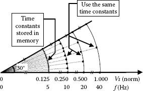
FIGURE 5.40 Operation within a 30° sector.

FIGURE 5.41 Spectra for different PWM patterns at 40 Hz. (a) Optimal PWM at fundamental frequency of 40 Hz. (b) Optimal SVM at fundamental frequency of 40 Hz.
(5.54) |
These values yield both fifth and seventh harmonics below 3% of the fundamental of the output voltage. These harmonic results are shown in Figure 5.41.
5.11 IMPROVING THE TRANSIENT RESPONSE IN HIGH-SPEED CONVERTERS
Numerous motor drives require operation at high speed, with fast transient response. This is achieved in control by applying as much voltage as possible within the actuator. Modern embedded controllers implement controller saturation and over-modulation operation in order to allow this increase in voltage.
In order to quantify this operation at highest voltage available, let us consider the induction machine drive with rotor in short-circuit as a symmetrical three-phase system with isolated neutral [47]. The stator voltage equation in complex variables yields:
(5.55) |
with
(5.56) |
(5.57) |
We can consider a reference system with ωλ = 0.
(5.58) |
The apparent power transferred between the inverter (actuator) and the electrical machine yields:
(5.59) |
In order to separate active and reactive (imaginary) power components, let us denote the phase shift between the stator voltage vs and the back-emf voltage e with φ. This yields into
(5.60) |
(5.61) |
The active power P is depending strongly on the angle φ, while the reactive power Q is mostly influenced by the magnitude of stator voltage (Vsλ).
During a fast change in the speed reference, the load torque needs to increase quickly to a maximum for an increase of speed and to decrease quickly to a minimum for a decrease in speed. During such a transient of the torque, there is a temporary transfer of reactive (imaginary) power between the mechanical system and the inverter (Figure 5.42). When the voltage applied (Vsλ) is higher, the amount of reactive energy (derived from power Q) transferred within the system yields lower. That is the inverter absorbs quicker the reactive energy from load. This yields into a faster transient.
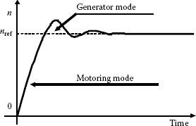
FIGURE 5.42 Explanation of the power transfer during transients.
This means that inverterized motor drives with higher voltage availability (or higher DC bus voltage) allow a faster transient of the drive. For a given voltage setup, the available applied voltage can be increased by control within certain limits. If such control is implemented within the embedded software, its speed depends on the sampling interval and the software arrangement. This usually yields in a fairly slow response. An alternative method [47,48] proposes to derive the additional voltage from the operation of the inverter with only two switches during the zero state intervals.
Observing the operation of the power converter with sinusoidal currents demonstrates that it is enough to control actively the current within two phases of the drive while the third current results from the current summation to zero within the neutral.
The proposed PWM algorithm is developed on the frame of a conventional space vector modulation algorithm while taking advantage of this property of currents. This controller uses two switches turned-on during a zero-state.
Depending on the value and direction of the third current, the uncontrolled inverter leg can go to the same DC potential with the other two producing a true zero voltage vector or can go on the other DC potential producing an active vector on the load. The phase current automatically determines the value of the voltage applied to the third phase of the load during the zero state.
Figure 5.43 shows the definition of the operation modes. Each state is defined with the conduction state (0 or 1) for each switch. The first set of three numbers correspond to the high-side switches, and the next set of three numbers correspond to the low-side switches. The uncontrolled switches are also shown in the figure as 0, while the other switches can take any value (0 or 1) according to the PWM algorithm. For more detail, all possible states are shown organized in Table 5.2. The same data is shown in Table 5.3 based on the phase of the current vector for the case of a PWM using a single zero state vector on each sampling interval
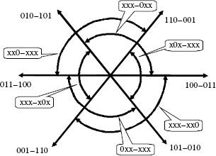
FIGURE 5.43 Definition of the inverter switching states.
α = angular coordinate of desired voltage vector within the 60° sector.
ϕ = phase shift between voltage vector and current vector.
For instance, the additional voltage ΔV contributed when operation takes place within the first sector (0° to 60°) is superimposed to the expected voltage vector. It can be calculated by averaging formulas.
If ϕ < 90 ⇒ Ia > 0 ⇒ ΔV = 0
If 90 < ϕ < 150
For α < ϕ − 90 ⇒ Ia < 0 ⇒ V = V1 and
(5.62) |
TABLE 5.2
Voltage Vectors Generated During the Zero Vector States Based on Phase Current’s Polarity
Sector 1: 0–60° |
Zero vector 0-0-0 |
000-011 |
Ia ≥ 0 ⇒ V = 0 |
Ia ≤ 0 ⇒ V = V1 |
Zero vector 1-1-1 |
101-000 |
Ib ≥ 0 ⇒ V = V6 |
Ib ≤ 0 ⇒ V = 0 |
|
Sector 2: 60–120° |
Zero vector 0-0-0 |
000-011 |
Ia ≥ 0 ⇒ V = 0 |
Ia ≤ 0 ⇒ V = V1 |
Zero vector 1-1-1 |
110-000 |
Ic ≥ 0 ⇒ V = V2 |
Ic ≤ 0 ⇒ V = 0 |
|
Sector 3: 120–180° |
Zero vector 0-0-0 |
000-101 |
Ib ≥ 0 ⇒ V = 0 |
Ib ≤ 0 ⇒ V = V3 |
Zero vector 1-1-1 |
110-000 |
Ic ≥ 0 ⇒ V = V2 |
Ic ≤ 0 ⇒ V = 0 |
|
Sector 4: 180–240° |
Zero vector 0-0-0 |
000-101 |
Ib ≤ 0 ⇒ V = 0 |
Ib ≥ 0 ⇒ V = V3 |
Zero vector 1-1-1 |
011-000 |
Ia ≥ 0 ⇒ V = V4 |
Ia ≤ 0 ⇒ V = 0 |
|
Sector 5: 240–300° |
Zero vector 0-0-0 |
000-110 |
Ic ≥ 0 ⇒ V = 0 |
Ic ≤ 0 ⇒ V = V5 |
Zero vector 1-1-1 |
011-000 |
Ia ≥ 0 ⇒ V = V4 |
Ia ≤ 0 ⇒ V = 0 |
|
Sector 6: 300–360° |
Zero vector 0-0-0 |
000-110 |
Ic ≥ 0 ⇒ V = 0 |
Ic ≤ 0 ⇒ V = V5 |
Zero vector 1-1-1 |
101-000 |
Ib ≥ 0 ⇒ V = V6 |
Ib ≤ 0 ⇒ V = 0 |
TABLE 5.3
Generation of Voltage Vectors Based on the Current Vector Phase
Sector |
Zero Vector 0-0-0 |
|
0–60° |
ϕ < 90 ⇒ |
⇒ Ia > 0 ⇒ V = 0 |
90 < ϕ < 150 ⇒ |
||
(a) For α < ϕ −90 |
⇒ Ia < 0 ⇒ V = V1 |
|
(b) For 60 > α > ϕ −90 |
⇒ Ia > 0 ⇒ V = 0 |
|
ϕ > 150 ⇒ |
⇒ Ia < 0 ⇒ V = V1 |
|
120–180° |
ϕ < 90 ⇒ |
⇒ Ib > 0 ⇒ V = 0 |
90 < ϕ< 150 ⇒ |
||
(a) For α < ϕ −90 |
⇒ Ib < 0 ⇒ V = V3 |
|
(b) For 60 > α > ϕ −90 |
⇒ Ib > 0 ⇒ V = 0 |
|
ϕ > 150 ⇒ |
⇒ Ib < 0 ⇒ V = V3 |
|
240–300° |
ϕ < 90 ⇒ |
⇒ Ic > 0 ⇒ V = 0 |
90 < ϕ< 150 ⇒ |
||
(a) For α < ϕ −90 |
⇒ Ic < 0 ⇒ V = V5 |
|
(b) For 60 > α > ϕ −90 |
⇒ Ic > 0 ⇒ V = 0 |
|
ϕ > 150 ⇒ |
⇒ Ic < 0 ⇒ V = V5 |
|
Sector |
Zero Vector 1-1-1 |
|
60–120° |
ϕ < 90 ⇒ |
⇒ Ic < 0 ⇒ V = 0 |
90 < ϕ< 150⇒ |
||
(a) For α < ϕ −90 |
⇒ Ic > 0 ⇒ V = V2 |
|
(b) For 60 > α > ϕ −90 |
⇒ Ic < 0 ⇒ V = 0 |
|
ϕ > 150 ⇒ |
⇒ Ic > 0 ⇒ V = V2 |
|
180–240° |
ϕ < 90 ⇒ |
⇒ Ia < 0 ⇒ V = 0 |
90 < ϕ< 150 ⇒ |
||
(a) For α <ϕ −90 |
⇒ Ia > 0 ⇒ V = V4 |
|
(b) For 60 > α > ϕ −90 |
⇒ Ia < 0 ⇒ V = 0 |
|
ϕ > 150 ⇒ |
⇒ Ia > 0 ⇒ V = V4 |
|
300–360° |
ϕ < 90 ⇒ |
⇒ Ib < 0 ⇒ V = 0 |
90 < ϕ< 150 ⇒ |
||
(a) For α < ϕ −90 |
⇒ Ib > 0 ⇒ V = V6 |
|
(b) For 60 > α > ϕ −90 |
⇒ Ib < 0 ⇒ V = 0 |
|
ϕ > 150 ⇒ |
⇒ Ib > 0 ⇒ V = V6 |
|
For 60 > α > ϕ −90 ⇒ Ia > 0 ⇒ ΔV = 0
If ϕ > 150 ⇒ Ia < 0 ⇒ V = V1 and
(5.63) |
Exploiting these equations for all sectors yields the graphical representation from Figure 5.44 for the additional voltage. All this additional voltage is induced naturally without any special software algorithm except the new definition of the zero states. Furthermore, the conventional operation of a space vector modulation algorithm is not modified at a current phase shift below 90°.
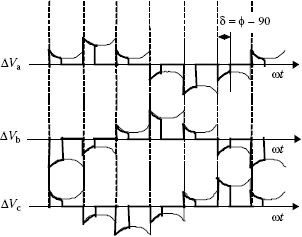
FIGURE 5.44 Additional voltage due to current-voltage phase shift.
To quantify further this method, calculation is done for the steady-state operation at a given modulation index m and the same phase shift ϕ (constant) over the entire fundamental period of the generated voltage. The RMS of the additional voltage can be calculated as a function of the phase shift δ = ϕ − 90 and required modulation index m:
(5.64) |
(5.65) |
This dependency is represented in Figure 5.45, and it represents an ideal maximum voltage. During the transient operation, the phase shift changes regularly and the additional voltage also changes. This helps understanding the limits and advantages of this method and assessing the usability in real industrial applications. The effects of using this modified PWM algorithm are shown in Figure 5.46.
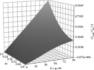
FIGURE 5.45 Additional voltage in respect to the current-voltage phase shift and modulation index.
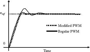
FIGURE 5.46 Results based on the mathematical model (speed as reference).
The space vector theory has been known for more than half a century, but only during the last 20 years, it has been consistently used in the control of three-phase converters. Details of PWM generation on the basis of vector representation as well as use of this concept in motor drives are the subjects of this chapter. All SVM variations are reviewed and the advantages of discontinuous reference functions are also outlined.
P5.1 |
Write relationship for Park/Clarke direct transforms and inverse transforms and prove the meaning of coefficients for power conservation and for magnitude conservation. |
P5.2 |
Establish the mathematical expressions for waveforms in Figure 5.26. Consider each one as a phase function and write the mathematical expressions for the other two phases taking into account the phase shifts of 120° and 240°. |
P5.3 |
Consider functions defined in P4.2. and define a new base in the vector space similar to the base defined in Equations 5.4, 5.5, 5.6. Then define a vector transform able to convert the (d, q, 0) quasi-DC coordinates into phase voltages as shaped in Figure 2.22. Use a computer program (MathCAD, Matlab) to implement these relationships and run the program to plot control functions. |
P5.4 |
Imagine a PWM pattern synchronized with the fundamental period and a count of 24 pulses on one period: • Draw the spatial distribution of the tip of the voltage vector. • For each discrete position thus determined, calculate the amount of time associated with each neighboring active vectors using Equations 5.29 and 5.30 for a modulation index of 0.55 defined as in Equation 5.31. • Consider the active vectors in the middle of the sampling interval and draw the time evolution of the voltage on the first phase during the first sector (Method D-I-H), using information from Figure 5.13. |
P5.5 |
If a three-phase inverter is supplied from a three-phase central-point rectifier with very weak filtering or without filtering, calculate the maximum voltage we can have at the inverter output without overmodulation. Use Figure 5.11 and Equation 5.31 after definition of the minimum value of the rectified voltage (VDC). Consider the grid RMS voltage as 120 V per phase. |
P5.6 |
|
P5.7 |
Write Equation 5.48 for each sector, using the active switching vectors from Figure 5.13 and their ortho-normal coordinates in the complex plane. |
P5.8 |
Use Figure 5.23 and define the instants for turning ON each of the six IGBT switches. • Write their expressions as a delay from the beginning of the sampling interval: For instance, f(S1) = t0/2, f(S2) = Ts − t0/2, and so on. Replace definitions from Equations 5.41, 5.42, 5.43, 5.44, 5.45, 5.46 for each sector. Organize these results as a flowchart to be implemented in a micro-controller with a center-aligned PWM generator. • Write a computer program and draw the evolution of the calculated ON-time. Compare the results with Figure 5.15. |
P5.9 |
Do the same as in P.5.7. with the switching sequence shown in Figure 5.28. Compare results with Figure 5.29. |
P5.10 |
Explain an algorithm to take advantage of the best HCF from Figures 5.30 and Figure 5.32. How can we modify the switching reference function to ensure a smooth transition from one method to another? |
1. Park, R.H. 1929/1933. Two-reaction theory of synchronous machines. AIEE Transactions. No. 48, pp. 716–730 and no. 52, pp. 352–355.
2. Kron, G. 1942. The application of tensors to the analysis of rotating electrical machinery, Schenectady, NY, USA, General Electric Review.
3. Stanley, H.C. 1938. An analysis of the induction motor. AIEE Trans. 57, 751–755.
4. Kovacs, K.P. and Racz, I. 1959. Transiente Vorgange in Wechselstrommachinen. Budapest, Hungary, Akad Kiado.
5. Stepina, J. 1967. Raumzeiger als Grundlage der Theorie der Elktrischen Maschinen. etz-A 88(23), 584–588.
6. Serrano-Iribarnegaray, L. 1993. The modern space-phasor theory, Part I & Part II. ETEP J. 3(2), March/April, 3 May/June.
7. Murai, Y. and Tsunehiro, Y. 1983. Improved PWM method for induction motor drive inverters, IPEC, Tokyo, pp. 407–417.
8. Holtz, J., Lammert, P., and Lotzkat, W. 1986. High speed drive system with ultrasonic MOSFET-PWM-inverter and single-CHIP microprocessor control. Conference Record 1986 IEEE Industry Applications Society Annual Meeting, Part 1, Denver, Colorado, USA, pp. 12–17.
9. Van der Broeck, H.W., Skudelny, H.C., and Stanke, G. 1986. Analysis and realization of a pulse width modulator based on voltage space vectors. IEEE-IAS Annual Meeting Conference Record, Denver, USA, pp. 244–251.
10. Fukuda, S., Hasegawa, H., and Iwaiji, Y. 1988. PWM technique for inverter with sinusoidal output current. 19th Annual IEEE Power Electronics Specialists Conference, Kyoto, Japan, vol. 1, 11–14 April, pp. 35–41.
11. Granado, J., Harley, R.G., and Diana, G. 1989. Understanding and designing a space vector pulse-width-modulator to control a three phase inverter. Trans. SAIEE 80, 29–37.
12. Halmos, P. 1986. Finite-Dimensional Vector Spaces. Springer-Verlag, New York.
13. Abrahamsen, J., Pedersen, J.K., and Blaabjerg, F. 1996. State-of-the-art of optimal efficiency control of low cost induction motor drives. PEMC’96, vol. 2, Budapest, Hungary, 2–4 September, pp. 163–170.
14. Murai, Y., Gohshi, Y., Matsui, K., and Hosono, I. 1992. High-frequency split zero-vector PWM with harmonic reduction for induction motor drive. Trans. IA 28(1), 105–112.
15. Murai, Y., Sugimoto, S., Iwasaki, H., and Tsunehiro, Y. 1983. Analysis of PWM inverter fed inductions motors for microprocessors. Proceedings IEEE/IECON, San Francisco, CA, USA, 10–14 November, pp. 58–63.
16. Fukuda, S., Iwaji, Y., and Hasegawa, H. 1990. PWM technique for inverter with sinusoidal output current. IEEE Trans. PE 5, 54–61.
17. Andersen, E.C. and Hann, A. 1993. Influence of the PWM control method on the performance of frequency inverter induction machine drives. ETEP 3(2), 151–160.
18. Holtz, J. 1992. Pulsewidth modulation—A survey. IEEE Trans. IE 39(5), 410–420.
19. Holtz, J. 1994. Pulsewidth modulation for electronic power conversion. Proc. IEEE 82(8), 1194–1212.
20. Handley, P.G. and Boys, J.T. 1991. Space vector modulation—An engineering review. PEVSD, London, UK, 87–91.
21. Neacsu, D. 2001. Space vector modulation. Seminar IEEE-IECON, San Jose, CA, USA, December.
22. Neacsu, D., Stincescu, R., Raducanu, I., and Donescu, V. 1994. Fuzzy logic control of a PWM V/f inverter-fed drive. ICEM’94, vol. 3, Paris, France, pp. 12–17.
23. Saetieo, S. and Torrey, D. 1998. Fuzzy logic control of a space vector PWM current regulator for three-phase power converter. IEEE Trans. PE 13(3), 419–426.
24. Enjeti, P. and Shireen, A. 1992. A new technique to reject DC-link voltage ripple for inverters operating on programmed PWM waveforms. IEEE Trans. PE 7(1), 171–180.
25. Schermann, M. and Schroedl, M. 1993. Methods of generating the voltage space vector by fast real-time PWM. IEEE-PCC, Yokohama, Japan, pp. 322–327.
26. Jacobina, C.B., Nogueira Lima, A.M., da Silva, E.R.C., Alves, R.N.C. and Seixas, P.F. 2001. Digital scalar pulse-width modulation: A simple approach to introduce non-sinusoidal modulating waveforms. IEEE Trans. PE 16(3), 351–359.
27. Lai, Y.S. and Bowes, S.R. 1996. A universal space vector modulation strategy based on regular-sampled pulse-width modulation [invertors]. Proceedings IEEE IECON, 22nd, vol. 1, pp. 120–126.
28. Bowes, S.R. and Lai, Y.S. 1997. The relationship between space-vector modulation and regular-sampled PWM. IEEE Trans. IE 44(5), 670–679.
29. Sun, J. and Grotstollen, H. 1996. Optimized space vector modulation and regular-sampled PWM: A re-examination. Conference Record of the 1996 IEEE Thirty-First IAS Annual Meeting IAS ’96, San Diego, CA, USA, vol. 2, pp. 956–963, 6–10 October.
30. Holmes, D.G. 1992. A unified modulation algorithm for voltage and current source inverters based on AC–AC matrix converter theory. IEEE Trans. IA 28(1), 31–40.
31. Neacsu, D. and Lucanu, M. 1992. Output waveform optimization of the SVM inverters. Proceedings of National Conference Electric Drives, Iasi, Romania, 22–24, October, pp. B1–B6.
32. Holmes, D.G. 1995. The significance of zero space vector placement for carrier based PWM schemes. Conference Record of the Thirtieth IAS Annual Meeting IEEE Industry Applications Conference, IAS ’95, Orlando, FL, USA, vol. 3, pp. 2451–2458, 8–12 October.
33. Kolar, J.W., Ertl, H, and Zach, F.C. 1989. Calculation of the passive and active component stress of three-phase PWM converter. Proceedings EPE, Aachen, Germany, pp. 1303–1311.
34. Alexander, D.R. and Williams, S.M. 1993. An optimal PWM algorithm implementation in a high performance 125 kVA inverter. Conference Proceedings of the 1993 Eighth Annual Applied Power Electronics Conference and Exposition, APEC ’93, San Diego, CA, USA, pp. 771–777, 7–11 March.
35. van der Broeck, H.W. 1991. Analysis of the harmonics in voltage-fed inverter drives caused by PWM schemes with discontinuous switching operation. Proceedings EPE ’91, pp. 3/261–3/266.
36. Houldsworth, J.A. and Grant, D.A. The use of harmonic distortion to increase the output voltage of a three-phase PWM inverter. IEEE Trans. IA IA-20, 1224–1228.
37. Hava, A.M., Kerkman, R.J., and Lipo, T.A. 1998. A high performance generalized discontinuous PWM algorithms. IEEE Transactions on Industry, Applications, vol. 34, no. 5, pp. 1059–1071, September–October.
38. Trzynadlowski, A.M. and Legowski, S. 1994. Minimum-loss vector PWM strategy for three-phase inverters. IEEE Trans. PE 9(1), 26–34.
39. Chung, D.W. and Sul, S.L. 1997. Minimum-loss PWM strategy for a 3-phase PWM rectifier. Proceedings of the 28th Power Electronics Specialists Conference PESC, St. Louis, MO, USA, vol. 2, pp. 1020–1026, 22–27 June.
40. Lai, R.S. and Ngo, K.D.T. A PWM method for reduction of switching loss in a full-bridge inverter. IEEE Trans. PE 10(3), 326–332.
41. Trzynadlowski, A.M., Kirlin, R.L., and Legowski, S. Space vector PWM technique with minimum switching losses and a variable pulse rate. IEEE Trans. IE 44(2), 173–181.
42. Faldella, E. and Rossi, C. 1994. High efficiency PWM techniques for digital control of DC/AC converters. Conference Proceedings of the Ninth Annual Applied Power Electronics Conference and Exposition, APEC ’94, Orlando, FL, vol. 1, pp. 115–121, February 13–17.
43. Perruchoud, P.J.P. and Pinewski, P.J. 1996. Power losses for space vector modulation techniques. IEEE-WPET, Dearborn, MI, USA, pp. 167–173.
44. Ahmad, R.H., Karady, G.G., Blake, T.D., and Pinewski, P. 1997. Comparison in space vector modulation techniques based on performance indexes and hardware implementation. 23rd International Conference on Industrial Electronics, Control and Instrumentation, IECON 97, New Orleans, LA, USA, vol. 2, pp. 682–687, 9–14, November.
45. Lucanu, M. and Neacsu, D. 1995. Optimal V/f control for space vector PWM three-phase inverters. Eur. Trans. EPE 5(2), 115–120.
46. Prasad, V.H., Borojevic, D., and Dubovsky, S. 1997. Comparison of high-frequency PWM algorithms for voltage source inverters. Conference Proceedings of the 13th Annual Applied Power Electronics Conference and Exposition, APEC 1997, Atlanta, GA, USA, pp. 857–863, 23–27 February.
47. Neacsu, D.O. 2007. Mathematical model for induction machine drives with modified PWM. IEEE Int’l Symposium SCS, 2007, pp.1–4.
48. Lucanu, M., and Neacsu, D. 1992. Optimization of the controller synthesis for three-phase inverters using space vector pulse width modulator. The Transactions of the SAIEE, vol. 83, no. 2, June 1992, pp.113–117.